Denon S-102 Service Manual
Dvd home entertainment system
Hide thumbs
Also See for S-102:
- Service manual (125 pages) ,
- Owner's manual (54 pages) ,
- Specifications (2 pages)
Advertisement
Quick Links
QQ
3 7 63 1515 0
S-102
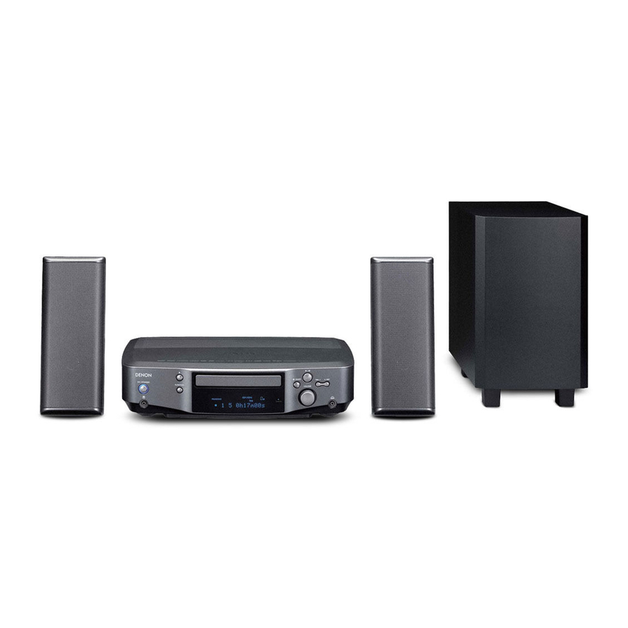
HOME ENTERTAINMENT SYSTEM (S-102) consists of DVD SURROUND RECEIVER
(ADV-S102), SUB WOOFER (DSW-S102) and SPEAKER SYSTEM (SC-S102)
TE
L 13942296513
For purposes of improvement, specifications and
design are subject to change without notice.
Please use this service manual with referring to the
operating instructions without fail.
Some illustrations using in this service manual are
slightly different from the actual set.
www
.
http://www.xiaoyu163.com
SERVICE MANUAL
MODEL
DVD HOME ENTERTAINMENT SYSTEM
x
ao
y
i
Denon Brand Company, D&M Holdings lnc.
http://www.xiaoyu163.com
8
JP
E3
E2
Q Q
3
6 7
1 3
u163
TOKYO, JAPAN
.
2 9
9 4
2 8
Ver. 2
Please refer to the
MODIFICATION NOTICE.
EK
E2A E1C E1K EUT
1 5
0 5
8
2 9
9 4
m
co
X0341 V.02 DE/CDM 0710
9 9
2 8
9 9
Advertisement

Related Manuals for Denon S-102


Summary of Contents for Denon S-102
- Page 1 MODEL E2A E1C E1K EUT S-102 DVD HOME ENTERTAINMENT SYSTEM HOME ENTERTAINMENT SYSTEM (S-102) consists of DVD SURROUND RECEIVER (ADV-S102), SUB WOOFER (DSW-S102) and SPEAKER SYSTEM (SC-S102) L 13942296513 For purposes of improvement, specifications and design are subject to change without notice.
- Page 2 S-102 3 7 6 3 1 5 1 5 0 SAFETY PRECAUTIONS The following check should be performed for the continued protection of the customer and service technician. LEAKAGE CURRENT CHECK Before returning the unit to the customer, make sure you make either (1) a leakage current check or (2) a line to chassis resistance check.
- Page 3 S-102 DIMENSION 3 7 63 1515 0 ADV-S102 0.5 max. L 13942296513 122.5 u163 http://www.xiaoyu163.com...
- Page 4 S-102 DSW-S102 3 7 63 1515 0 L 13942296513 u163 http://www.xiaoyu163.com...
- Page 5 S-102 SC-S102 3 7 63 1515 0 L 13942296513 u163 http://www.xiaoyu163.com...
- Page 6 S-102 WIRE ARRANGEMENT 3 7 63 1515 0 If wire bundles are untied or moved to perform adjustment or parts replacement etc., be sure to rearrange them neatly as they were originally bundled or placed afterward. Otherwise, incorrect arrangement can be a cause of noise generation.
- Page 7 S-102 2. DSW-S102 3 7 63 1515 0 2. DSW-S102 Fasten the CX041 4P connector cord to the chassis with a clamp band. Fasten the CX041 4P connector cord and CX081 8P con- nector cord to the chassis with a clamp band.
- Page 8 S-102 DISASSEMBLY 3 7 63 1515 0 (Follow the procedure below in reverse order when reassembling.) ADV-S102 1. Loader Panel (1) Switch on, and press [ (OPEN/CLOSE)] button to open the Disc tray. (2) Detach the Loader Panel by lifting.
- Page 9 S-102 3. Top Cover 3 7 63 1515 0 (1) Remove 9 screws, then detach Top Cover. 4. DVD Mecha. Unit (1) Remove 4 screws fixing the DVD Mecha. (2) Detach the DVD Mecha. to the arrow direction. (3) Lift the DVD Mecha. and disconnect FFC and con- nectors.
- Page 10 S-102 5. Front Panel Ass’y 3 7 63 1515 0 (1) Remove 6 Front panel screws, then detach P.W.B. and chassis. (2) Remove 4 Front panel side screws, then detach the Front Panel Ass’y. L 13942296513 6. Back Panel Ass’y (1) Remove each terminal screws, Back Panel screws and Chassis screws, then detach the Back Panel.
- Page 11 S-102 DSW-S102 3 7 63 1515 0 1. Rear panel (1) Remove 10 screws 101 on the bottom side. (2) Detach the Rear panel. L 13942296513 2. SHIELD COVER (1) Remove 8 screws 103 on the Side. (2) Lift the shield cover using a flat-headed screwdriver and remove it.
- Page 12 S-102 DIAGNOSTICS OF OPTICAL PICKUP 3 7 63 1515 0 AND REPLACING TRAVERSE UNIT Make failure diagnostics of the Optical Pickup as follows. If the laser drive current (Iop) becomes more than 1.5 times of the initial value, the Optical Pickup should be replaced.
- Page 13 S-102 1. Iop checked Method 3 7 63 1515 0 Select the laser ON/OFF (CD/DVD) mode of the test mode, and check the lop value of DVD laser or CD laser. (See page 13 for test mode.) 1.1. DVD laser current check...
- Page 14 S-102 4. Rewriting the default value of the laser 3 7 63 1515 0 current To rewrite the default value of the laser current, press the button for at least 5 seconds while the CD or DVD laser current is displayed, then press the button to select T23.
- Page 15 S-102 HOW TO REPLACE TRAVERSE UNIT 3 7 6 3 1 5 1 5 0 3. Traverse Unit disassembly (1) Remove 24P FFC, 15P FFC and 5P PH WIRE connect- Caution: The optical pickup can be damaged easily by ing with from the Main P.W.B.
- Page 16 S-102 SERVICE MODE 3 7 6 3 1 5 1 5 0 1. Aging Mode 1.1. preparation0 (1) Equipment used: Any one of DVD Karaoke Disc (containing more than 10 titles). (ex : Heat run disc TDV-HR01) (2) Unit setting : No spec other than the following procedure.
- Page 17 S-102 2. Initial Setting Mode 3 7 6 3 1 5 1 5 0 2.1. Preparation (1) Equipment used: None (2) Unit setting: No spec other than the following procedure. 2.2. Procedure SYSTEM This initializes the data for the function, volume, DVD mechanism, etc.
- Page 18 S-102 4. Test mode 3 7 6 3 1 5 1 5 0 4.1. Entering the test mode To enter the test mode, press the buttons simultaneously while in the Aging mode. Not insert the disc. (The Aging mode is entered by pressing the buttons simultaneously to turn on the AC power.
- Page 19 S-102 4.3. Setting the mode 3 7 6 3 1 5 1 5 0 With the mode selected, press the button to set that mode. In the laser on/off (CD/DVD) mode, laser on/off control is executed and the laser current is displayed.
- Page 20 S-102 4.4. Change within the mode 3 7 6 3 1 5 1 5 0 Changes within modes are made by pressing the buttons while the mode is set. In the laser on/off (CD/DVD) mode, laser on/off control is executed and the laser current is displayed.
- Page 21 S-102 4.5. Execution of trace mode (error rate display) (See "Table 2 - Trace mode details") 3 7 6 3 1 5 1 5 0 Trace will be performed if the button is pushed after choosing operation. (YY : selection mode [71 to 94], m : address [PBA][HEX], l : error rate [COUNT/SEC] [HEX]) Note) CD : Error rate of 75 frames is displayed (1 second).
- Page 22 S-102 3 7 6 3 1 5 1 5 0 Table 2: Trace mode details Contents Contents supplement A display of PO error detection number of the inner circumference It is invalid at the time of CD operation. of 1-layer and an address.
- Page 23 S-102 3 7 6 3 1 5 1 5 0 TROUBLE SHOOTING ADV-S102 ADV 1 1. 1U-3836 (MAIN UNIT) 1.1. FL TUBE dosen't light (1) Check the Set-up process of System -COM Check Power Supply Voltages. 1U-3836-1(MAIN UNIT) [IC303]: Check Soldering.
- Page 24 S-102 3 7 6 3 1 5 1 5 0 (2) Check the Set-up process of B/E -COM Check Power Supply Voltages. 1U-3836-1(MAIN UNIT) Check Soldering. [IC101]: [IC304] +3.3V_D2,+2.0V_ESS O.K.? [IC111] O.K. Check Clock waveform. Check 27MHz(3.3V)at (1) Check Soldering. of X101.
- Page 25 S-102 3 7 6 3 1 5 1 5 0 1.2. No Sound,Noise generated [No Play], [00 00] displayed etc. (1) CD,DVD PLAY (1) Check Soldering of P.U. short-circuit? Check the Emission of Pick-up. (2) Check the circumference soldering of TR603 IU-3807(FEP UNIT) and TR604.
- Page 26 S-102 3 7 6 3 1 5 1 5 0 1.3. No Sound,Noise generated (1) CD,DVD PLAY Check Power Supply Voltages. 1U-3836(MAIN UNIT) Check Soldering. +12V_A1,-12V_A1 IC602,IC603 +7V,-7V of [IC601] IC404 +1.2V_DSP of [IC401] O.K. Check Reset signal of [IC401], [IC501],[IC502].
- Page 27 S-102 3 7 6 3 1 5 1 5 0 Check Analog Audio Data output from CODEC to AMP. Check Soldering. 1U-3836(MAIN UNIT) [IC501]:28,29,31pin [IC501]output and [IC506],[IC507] [IC506],[IC507] [FL],[FR],[SW] O.K. Check audio mute signal. Check Soldering. 1U-3836(MAIN UNIT) [IC503]:86pin...
- Page 28 S-102 3 7 6 3 1 5 1 5 0 (2) Analog audio in(AUX1,AUX2) Check Analog Audio Data input from AUX1-2 to FUNC.VR. Check Soldering. Check Analog Audio Data input 1U-3836(MAIN UNIT) JK601 from AUX1-2 to FUNC.VR. Check Soldering.
- Page 29 S-102 3 7 6 3 1 5 1 5 0 3. 1U-3836-1 (MAIN UNIT) 3. 1U-3836-1 (MAIN UNIT) 3-1.DVD PLAY 3-1.DVD PLAY (1) INTERLACE output does not outputed. (1) INTERLACE output does not outputed. Check Power Supply Voltages. Check Soldering.
- Page 30 S-102 3 7 6 3 1 5 1 5 0 Check analog signal for Video Check Soldering. from ENCODER to Video driver(COMPONENT) [IC801]37-39pin 1U-3836-1(MAIN UNIT) VR803-805 [IC801]output and [IC802]input: TR803-805 [Py],[Pb],[Pr] [IC802]11,13,15pin O.K. Check analog signal for Video Check Soldering.
- Page 31 S-102 3 7 6 3 1 5 1 5 0 (2) PROGRESSIVE output does not outputed. Check Digital signal for Video from B/E to I/P Check Soldering. Check Digital signal for Video 1U-3836-1(MAIN UNIT) [IC101]106-119pin from B/E to I/P Check Soldering.
- Page 32 S-102 3 7 6 3 1 5 1 5 0 (3) HDMI output does not outputed. (3) HDMI output does not outputed. Check Power Supply Voltages. Check Power Supply Voltages. 1U-3836-1(MAIN UNIT) Check Soldering. 1U-3836-1(MAIN UNIT) Check Soldering. [IC704]:+1.8V IC708 [IC704]:+1.8V...
- Page 33 S-102 3 7 6 3 1 5 1 5 0 3-2.AUX IN (1) Conposite INPUT Check Power Supply Voltages. Check Soldering. 1U-3836-1(MAIN UNIT) CX142 ±5V_V1 O.K. Check analog signal for Video Check Soldering. from connector to Video selector JK301...
- Page 34 S-102 3 7 6 3 1 5 1 5 0 (2) Y/C INPUT ower upp y l Vo ltages. Check Soldering. 1U-3836-1(MAIN UNIT) CX142 ±5V_V1 O.K. Check analog signal for Video Check Soldering. from connector to Video selector JK301...
- Page 35 S-102 DSW-S102 3 7 6 3 1 5 1 5 0 1. 1U-3811 (D.AMP/SMPS UNIT) 1. 1U-3811 (D.AMP/SMPS UNIT) (1) AMPLIFER Check the following parts (and surrounding area) and Check Reset signal. their soldering. N.G. (IC208 4pin) • [IC208] (BD4730) "H"...
- Page 36 S-102 (2) WAVEFORM 3 7 6 3 1 5 1 5 0 Waveform 1:Clock Waveform (24.576MHz) Waveform 4: A D Waveform 1 CH1:IC201 24pin 1 3 9 4 2 2 9 6 5 1 3 Waveform 2:PWM Signal (Pulse width changed by input signal)
- Page 37 S-102 3 7 6 3 1 5 1 5 0 (3) POWER SUPPLY Check Primary Parts and Soldering • [D405] (GSIB660) Check FUSE Condition • [IC401] (SW_TRANS) N.G. • FUSE (F401)OPEN? • [C432] (330/400) for E2 (1000/200) for E3/J •...
- Page 38 S-102 3 7 6 3 1 5 1 5 0 Check the following parts (and surrounding area) and Check +12V_A Output their soldering. • Voltage Check • [T401] (SW_TRANS) N.G. +12V_A DC (non-switched) Voltage is O.K.? • [IC403] (KIA7812API) (IC403 O Terminal (Output Terminal)) •...
- Page 39 S-102 ELECTRICAL ADJUSTMENT FOR VIDEO 3 7 63 1515 0 1. SETTING (1) Connect the monitor TV to the video output terminal. (2) Connect the oscilloscope to the Y-signal and C-signal of S-VIDEO output terminal and each terminate at 75 Ohms.
- Page 40 S-102 3. PROCEDURE 3 7 63 1515 0 (1) Adjust the signal of S-VIDEO out by the wave of oscillo- scope. (a) Target, Y-signal Point VR801 Adjustment Value 1000 20mV Waveform Y-signal of S-VIDEO out (b) Target, C-signal Point...
- Page 41 S-102 3 7 63 1515 0 (c) Target, P -signal Point VR805 Check Value 10mV Waveform -signal L 13942296513 u163 http://www.xiaoyu163.com...
- Page 42 S-102 BLOCK DIAGRAMS ADV-S102 3 7 6 3 1 5 1 5 0 1 3 9 4 2 2 9 6 5 1 3 w w w u 1 6 3 http://www.xiaoyu163.com...
- Page 43 S-102 DSW-S102 3 7 63 1515 0 L 13942296513 u163 http://www.xiaoyu163.com...
- Page 44 S-102 LEVEL DIAGRAM 3 7 63 1515 0 L 13942296513 u163 http://www.xiaoyu163.com...
- Page 45 S-102 SEMICONDUCTORS 3 7 63 1515 0 Only major semiconductors are shown, general semiconductors etc. are omitted to list. 1. IC’s ES6178FF (IC101: 1U-3836) PINOUT DIAGRAM HA2/AUX4[4] DSCK I2CDATA/AUX0 I2C_CLK/AUX1 DCS0# AUX2/IOW# DCS1# AUX3/IOR# DB15 AUX4 DB14 AUX5 DB13...
- Page 46 S-102 3 7 63 1515 0 ES6178FF PIN DESCRIPTION Name Pin Numbers Definition 1,18, 27, 59, 68, 75, 92, 99, 104, 130, I/O power supply. 148, 157, 159, 164, 183, 193, 201 2-7, 10-16, 19-23, LA[21:0] RISC port address bus.
- Page 47 S-102 3 7 63 1515 0 Name Pin Numbers Definition TSD0 Audio transmit serial data output 0. SEL_PLL0 Refer to the description and matrix for SEL_PLL2 pin 32. TSD1 Audio transmit serial data output 1. SEL_PLL1 Refer to the description and matrix for SEL_PLL2 pin 32.
- Page 48 S-102 3 7 63 1515 0 Name Pin Numbers Definition DCLK Clock input to PLL; (5V tolerant input). UDAC Video DAC output. F DAC V DAC Y DAC C DAC U DAC Value (pin 115) (pin 114) (pin 113)
- Page 49 S-102 3 7 63 1515 0 Name Pin Numbers Definition ADVEE Analog power for video DAC. ADVSS Analog ground for video DAC. YDAC Video DAC output. Refer to description and matrix for UDAC pin 106. YUV5 YUV pixel 5 output data PIXOUT5 CCIR656 output pixel 5.
- Page 50 S-102 3 7 63 1515 0 Name Pin Numbers Definition Host data bus line; (5V tolerant input). DCI_FDS# DVD input sector start; (5V tolerant input). AUX2[0] Aux2 data I/O; (5V tolerant input). VFD_CLK VFD clock input. Host data bus line; (5V tolerant input).
- Page 51 S-102 3 7 63 1515 0 Name Pin Numbers Definition HWR# Host write. DCI_CLK DVD channel data clock; (5V tolerant input). AUX4[5] Aux4 data I/O; (5V tolerant input). HRD# Host read. DCI_ACK# DVD channel data valid; (5V tolerant input).
- Page 52 S-102 3 7 63 1515 0 DSP21367 (IC401: 1U-3836) L 13942296513 u163 http://www.xiaoyu163.com...
- Page 53 S-102 3 7 63 1515 0 M30627FHPGP (IC301: 1U-3836) L 13942296513 Port Port Port Name Explanation Function setting VREF VREF Reference Voltage Input for A/D converter AVCC AVCC Positive power P97/SIN4 DSP_MISO Serial Data input from DSP P96/SOUT4 DSP_MOSI...
- Page 54 S-102 3 7 63 1515 0 Port Port Port Name Explanation Function setting P_DOWN( 50/60Hz ) 50Hz/60Hz AC input PWB_CHK Checking PWB input /SMONI_SELB SelecteYC Video outputB /SMONI_SELA Selecte YC Video outputA VOL_B VOL encoder Pulse-B input VOL_A VOL encoder Pulse-A input...
- Page 55 S-102 3 7 63 1515 0 Port Port Port Name Explanation Function setting P123 SAN_MOSI Serial Data output to TUNER/RDS IC P122 /CODEC_RST Reset output to CODEC P121 PRE_MUTE_SUB MUTE output to PRE OUT. H:MUTE P120 HP_MUTE_SUB MUTE output to HEAD PHONE output. H:MUTE...
- Page 56 S-102 3 7 63 1515 0 W9864G2GH-7 (IC402: 1U-3836) PIN DESCRIPTION PIN NAME FUNCTION DESCRIPTION Address Multiplexed pins for row and column address. A0−A10 Row address: A0−A10. Column address: A0−A7. A10 is sampled during a precharge command to determine if all banks are to be precharged or bank selected by BS0, BS1.
- Page 57 S-102 3 7 63 1515 0 K4S641632 (IC103: 1U-3836) DQ15 DQ14 DQ13 DQ12 DQ11 DQ10 LDQM N.C/RFU UDQM A10/AP 54Pin TSOP (II) (400mil x 875mil) (0.8 mm Pin pitch) PIN FUNCTION DESCRIPTION Name Input Function Active on the positive going edge to sample all inputs.
- Page 58 S-102 3 7 63 1515 0 TAS5142DKD (IC206: 1U-3811) L 13942296513 u163 http://www.xiaoyu163.com...
- Page 59 S-102 3 7 63 1515 0 TAS5121DKD (IC207: 1U-3811) GVDD_B PWM_BP GVDD_B RESET BST_B DREG_RTN PVDD_B GVDD PVDD_B OUT_B DREG OUT_B DGND OUT_A DVDD OUT_A PVDD_A DGND PVDD_A BST_A PWM_AP GVDD_A GVDD_A Terminal Functions TERMINAL FUNCTION (1) FUNCTION (1)
- Page 60 S-102 3 7 63 1515 0 BU2360FV (IC109: 1U-3836) L 13942296513 BD7820 (IC111, IC707: 1U-3836) BLOCK DIAGRAM GND (FIN) P i n No . P in N am e V r e f C T L Driver V c c N .C .
- Page 61 S-102 2. FL DISPLAY 3 7 63 1515 0 15-BT-102GN Pin Connection Grid Assignment L 13942296513 Anode Connection u163 http://www.xiaoyu163.com...
- Page 62 S-102 PRINTED WIRING BOARDS 3 7 6 3 1 5 1 5 0 1U-3836 MAIN P.W.B. UNIT (1/2) 1 3 9 4 2 2 9 6 5 1 3 w w w u 1 6 3 COMPONENT SIDE http://www.xiaoyu163.com...
- Page 63 S-102 3 7 6 3 1 5 1 5 0 1U-3836 MAIN P.W.B. UNIT (2/2) 1 3 9 4 2 2 9 6 5 1 3 w w w u 1 6 3 FOIL SIDE http://www.xiaoyu163.com...
- Page 64 S-102 3 7 6 3 1 5 1 5 0 1U-3831 LOC/PWR-DISP P.W.B. UNIT (1/2) 1 3 9 4 2 2 9 6 5 1 3 w w w u 1 6 3 COMPONENT SIDE http://www.xiaoyu163.com...
- Page 65 S-102 3 7 6 3 1 5 1 5 0 1U-3831 LOC/PWR-DISP P.W.B. UNIT (2/2) 1 3 9 4 2 2 9 6 5 1 3 w w w u 1 6 3 FOIL SIDE http://www.xiaoyu163.com...
- Page 66 S-102 3 7 6 3 1 5 1 5 0 1U-3811 D.AMP/SMPS P.W.B. UNIT (1/2) 1 3 9 4 2 2 9 6 5 1 3 w w w u 1 6 3 COMPONENT SIDE http://www.xiaoyu163.com...
- Page 67 S-102 3 7 6 3 1 5 1 5 0 1U-3811 D.AMP/SMPS P.W.B. UNIT (2/2) 1 3 9 4 2 2 9 6 5 1 3 w w w u 1 6 3 FOIL SIDE http://www.xiaoyu163.com...
- Page 68 S-102 3 7 6 3 1 5 1 5 0 1U-3807 FEP P.W.B. UNIT 1 3 9 4 2 2 9 6 5 1 3 w w w u 1 6 3 FOIL SIDE COMPONENT SIDE http://www.xiaoyu163.com...
- Page 69 S-102 NOTE FOR PARTS LIST 3 7 63 1515 0 • Parts for which "nsp" is indicated on this table cannot be supplied. • When ordering of part, clearly indicate "1" and "I" (i) to avoid mis- supplying. •...
- Page 70 S-102 PARTS LIST OF P.W.B. UNIT 3 7 63 1515 0 Parts for which "nsp" is indicated on this table cannot be supplied. The parts listed below are for maintenance only, might differ from the parts used in the unit in appearances or dimensions.
- Page 71 S-102 3 7 63 1515 0 Ref. No. Part No. Part Name Remarks Q'ty New IC804,805 00D 262 3446 900 TC4052BFT IC806,807 00D 263 1296 906 TA48025BF(T6L1,NQ) IC901 00D 262 3360 905 LC72722PM-TLM for E2 TR201 00D 274 0188 905...
- Page 72 S-102 3 7 63 1515 0 Ref. No. Part No. Part Name Remarks Q'ty New RESISTORS GROUP R452,453 00D 241 2313 901 RD14B2E101GFRST R845 00D 244 2051 974 RS14B3A102JNBST(S) VR801-805 00D 211 6148 906 V03PB471MT(RH03ADCS) +REF CAPACITORS GROUP C101,102...
- Page 73 S-102 3 7 63 1515 0 Ref. No. Part No. Part Name Remarks Q'ty New C260 CK73F1E104ZT +1608 C276 CK73F1E104ZT +1608 C277 CK73B1H102KT +1608 C278 00D 254 4740 934 CE67W1C101MT(GV) C279 CK73F1E104ZT +1608 C281 CK73F1H103ZT +1608 C282 00D 254 4756 902...
- Page 74 S-102 3 7 63 1515 0 Ref. No. Part No. Part Name Remarks Q'ty New C429 CK73F1C104ZT +1005 C430 CK73B1H102KT +1005 C431 CK73F1C104ZT +1005 C432 00D 257 0039 910 CK73B0J226MT C433 CK73B1H102KT +1608 C434 CK73B1A106KT +2125 C435 CK73F1C104ZT +1005...
- Page 75 S-102 3 7 63 1515 0 Ref. No. Part No. Part Name Remarks Q'ty New C559 CK73B1H332KT +1608 C560 CK73F1E104ZT +1608 C561 CK73F1H103ZT +1608 C563 00D 254 4743 902 CE67W1H0R1MT(GV) C564 00D 254 4740 921 CE67W1C470MT(GV) C565 CK73F1E104ZT +1608...
- Page 76 S-102 3 7 63 1515 0 Ref. No. Part No. Part Name Remarks Q'ty New C758 00D 254 4742 929 CE67W1V220MT(GV) C759 CK73F1E104ZT +1608 C760 00D 254 4742 916 CE67W1V100MT(GV) C762 CC73CH1H470JT +1608 C763 00D 254 4742 929 CE67W1V220MT(GV)
- Page 77 S-102 3 7 63 1515 0 Ref. No. Part No. Part Name Remarks Q'ty New C913-928 CK73F1C104ZT +1005 C929 CK73F1H103ZT +1005 C930 CK73B1H102KT +1005 C931 CK73F1H103ZT +1005 C932 CK73F1C104ZT +1005 C933,934 CC73CH1H180JT +1608 C935 CK73F1H103ZT +1005 C936 00D 257 2018 900...
- Page 78 S-102 3 7 63 1515 0 Ref. No. Part No. Part Name Remarks Q'ty New CC119,120 CK73B1H102KT +1005 CC121 CK73F1C104ZT +1005 CC122 CK73B1H102KT +1005 CC123,124 CK73F1C104ZT +1005 CC125-129 CK73F1E104ZT +1608 CC139,140 CK73F1E104ZT +1608 CC141,142 00D 254 4740 921 CE67W1C470MT(GV)
- Page 79 S-102 3 7 63 1515 0 Ref. No. Part No. Part Name Remarks Q'ty New CC321 CC73CH1H101JT +1608 CC324 CC73CH1H101JT +1608 CC325 CK73F1E104ZT +1608 CC326 CK73F1H103ZT +1608 CC327 CK73B1E104KT +1608 CC328 CK73B1H103KT (1608) +1608 CC329 CK73B1E104KT +1608 CC330 00D 254 4740 976...
- Page 80 S-102 3 7 63 1515 0 Ref. No. Part No. Part Name Remarks Q'ty New CC938 CK73B1H102KT +1608 CC939 CK73F1E104ZT +1608 CC940 CK73F1H103ZT +1608 CC941 CK73B1H102KT +1608 CC942 CK73F1E104ZT +1608 CC943 CK73F1H103ZT +1608 CC944 CK73B1H102KT +1608 CC945 CK73F1E104ZT +1608...
- Page 81 S-102 3 7 63 1515 0 Ref. No. Part No. Part Name Remarks Q'ty New L201 00D 235 0166 003 INDUCTOR 100UH(7208M L301 00D 235 0186 902 INDUCTOR 47UH(7B12N) L302 00D 235 0185 903 INDUCTOR 47UH(7E10H) L303 00D 235 0186 902...
- Page 82 S-102 1U-3831D LOC/PWR-DSP P.W.B. UNIT ASS'Y 3 7 63 1515 0 Ref. No. Part No. Part Name Remarks Q'ty New SEMICONDUCTORS GROUP IC102 00D 263 1259 008 BA12T IC103 00D 263 1260 000 KIA79M12PI-U/P IC104 00D 263 1227 001...
- Page 83 S-102 3 7 63 1515 0 Ref. No. Part No. Part Name Remarks Q'ty New C133 CK73F1H103ZT +1608 C134 CK73B1H102KT +1608 C135 CK73F1E104ZT +1608 C136 CK73F1H103ZT +1608 C137 CK73B1H102KT +1608 C138 00D 254 4709 700 CE04W1V221MC JC5(KY) C140 CK73F1E104ZT...
- Page 84 S-102 3 7 63 1515 0 Ref. No. Part No. Part Name Remarks Q'ty New C208,209 CK73F1H103ZT +1608 C212 CK73F1H103ZT +1608 C221-224 CK73F1E104ZT +1608 C225,226 CK73B1H222KT +1608 C227,228 CK73F1E104ZT +1608 C241 CK73F1H103ZT +1608 C242,243 CK73F1E104ZT +1608 C244 00D 254 4737 947...
- Page 85 S-102 3 7 63 1515 0 Ref. No. Part No. Part Name Remarks Q'ty New FB111-114 00D 235 0049 900 BEADS INDUCTOR TAPE FB221-223 00D 235 0130 903 CHIP EMIFIL(11A121) +1608 FB291-293 00D 235 0130 903 CHIP EMIFIL(11A121) +1608...
- Page 86 S-102 1U-3811D/E/F D.AMP/SMPS P.W.B. UNIT ASS'Y 3 7 63 1515 0 Ref. No. Part No. Part Name Remarks Q'ty New SEMICONDUCTORS GROUP IC101-103 00D 263 1277 909 RC4580IDR IC201 00D 262 3502 909 TAS5066PAGRG4 IC202 00D 262 3504 907...
- Page 87 S-102 3 7 63 1515 0 Ref. No. Part No. Part Name Remarks Q'ty New D423 00D 276 0401 905 1SS133T77 (TAPE) D424 00D 276 0773 905 RB501V-40 +2125 D425 00D 276 0401 905 1SS133T77 (TAPE) D426,427 00D 276 0825 905...
- Page 88 S-102 3 7 63 1515 0 Ref. No. Part No. Part Name Remarks Q'ty New C132 00D 254 4722 936 CE04W1HR47MT(GR) C133 CK73B1H102KT +1608 C134 00D 254 4722 981 CE04W1H100MT(GR) C135 CC73CH1H101JT +1608 C136 CC73CH1H471JT +1608 C137 00D 254 4722 981...
- Page 89 S-102 3 7 63 1515 0 Ref. No. Part No. Part Name Remarks Q'ty New C281,282 CK73B1H104KT +2125 C283 CK73B1E333KT +1608 C284 CK73F1C105ZT +2125 C285-288 CK73B1H102KT +1608 C289,290 00D 254 4718 953 CE04W1C221MT(GR) C299-302 CK73B1H103KT (1608) +1608 C303-306 00D 254 4641 907...
- Page 90 S-102 3 7 63 1515 0 Ref. No. Part No. Part Name Remarks Q'ty New C442 00D 253 8029 700 CK45F2EAC222MC (KX) for E3, JP C443 CK73B1E104KT +1608 C444 00D 254 2708 701 CE04W1E471MC J16(KY) C445 00D 255 4261 720...
- Page 91 S-102 3 7 63 1515 0 Ref. No. Part No. Part Name Remarks Q'ty New F401 00D 206 1094 066 FUSE(233)T4AL125V for E3, JP F401 00D 206 1099 045 FUSE(02153.15MXP/250V) for E2 F402 00D 206 1094 053 FUSE(233)T3.15AL125V for E3, JP...
- Page 92 S-102 EXPLODED VIEW 3 7 6 3 1 5 1 5 0 30-1 1 3 9 4 2 2 9 6 5 1 3 WARNING: Parts marked with this symbol have critical characteristics. w w w Use ONLY replacement parts recommended by the manufacturer.
- Page 93 S-102 3 7 63 1515 0 PARTS LIST OF EXPLODED VIEW Parts for which "nsp" is indicated on this table cannot be supplied. ASS’Y ASS’Y P.W.B. ASS'Y for which "nsp" is indicated on this table cannot be supplied. When repairing the P.W.B. ASS'Y, check the board parts table and order replacement parts.
- Page 94 S-102 3 7 63 1515 0 Ref. No. Part No. Part Name Remarks Q'ty New CARD SPACER 00D 112 1000 001 VOLUME KNOB 00D 342 0040 003 FERRITE CRAMP081610N CORD HOLDER (L50) L=50 E2 LASER CAUTION for E2 LABEL(A) for E3 R.SHEET(E2) SUB ASSY...
- Page 95 S-102 EXPLODED VIEW OF DVD MECHANISM UNIT 3 7 6 3 1 5 1 5 0 WARNING: Parts marked with this symbol have critical characteristics. Use ONLY replacement parts recommended by the manufacturer. 1 3 9 4 2 2 9 6 5 1 3...
- Page 96 S-102 PARTS LIST OF DVD MECHANISM UNIT 3 7 63 1515 0 Parts for which "nsp" is indicated on this table cannot be supplied. The parts listed below are for maintenance only, might differ from the parts used in the unit in appearances or dimensions.
- Page 97 S-102 POINTS OF GREASING 3 7 6 3 1 5 1 5 0 With Cemedine 575, glue 3 joint parts of Clamper-L and H hooks. (0.05mg each x 3) *As for greasing to the R rail groove and groove's side edge, apply grease to the outer face "intentionally".
- Page 98 S-102 DSW-S102 EXPLODED VIEW 3 7 63 1515 0 L 13942296513 WARNING: Parts marked with this symbol have critical characteristics. Use ONLY replacement parts recommended by u163 the manufacturer. http://www.xiaoyu163.com...
- Page 99 S-102 DSW-S102 PARTS LIST OF EXPLODED VIEW 3 7 63 1515 0 Parts for which "nsp" is indicated on this table cannot be supplied. ASS’Y ASS’Y P.W.B. ASS'Y for which "nsp" is indicated on this table cannot be supplied. When repairing the P.W.B. ASS'Y, check the board parts table and order replacement parts.
- Page 100 S-102 3 7 63 1515 0 Ref. No. Part No. Part Name Remarks Q'ty New screws 0RD 473 3809 011 4X25 CBTS (1) 3X6 CBTS(S)-Z 3X6 CBTS(S)-B 3X8 CBTS (S)-B 3X10 CBTS (P)-Z 3X12 CBTS (P)-B 00D 477 0064 107...
- Page 101 S-102 SC-S102 PARTS LIST OF EXPLODED VIEW 3 7 63 1515 0 SC-S102 PARTS LIST OF EXPLODED VIEW Ref. No. Part No. Part Name Remarks Q'ty 00D 9H3 0001 727 SPEAKER SYSTEM(L&R) L 13942296513 u163 http://www.xiaoyu163.com...
- Page 102 S-102 PACKING VIEW 3 7 63 1515 0 18 19 L 13942296513 u163 http://www.xiaoyu163.com...
- Page 103 S-102 PARTS LIST OF PACKING & ACCESSORIES 3 7 63 1515 0 Parts for which "nsp" is indicated on this table cannot be supplied. The parts listed below are for maintenance only, might differ from the parts used in the unit in appearances or dimensions.
- Page 104 S-102 WIRING DIAGRAMS ADV-S102 3 7 6 3 1 5 1 5 0 H/P JACK Portable IN JACK S102 WIRING DIAGRAM FL Display 1U-3831 1U-3831 HP UNIT AUX IN UNIT 1U-3831 1U-3831 1U-3831 DISPLAY Left 5P SAN CW052 DISPLAY Right UNIT...
- Page 105 S-102 DSW-S102 3 7 63 1515 0 L 13942296513 CX041 CX151 CX081 (VH)WHT (PH) (PH) CY041 CY151 CY081 (VH)WHT (PH) (PH) CY021 (VH)WHT CY023 (VH)WHT DSUB25P SP TERMINAL u163 FEMALE http://www.xiaoyu163.com...
- Page 106 S-102 MEASURING METHOD AND WAVEFORMS 3 7 63 1515 0 To check the waveforms on the FEP, the GND (-) probe of the oscilloscope to “VHALF” point. (Except for lnner SW, TRVSW) NOTES Measuring Disc: DVD/VT502 or TDV-520A CD/TCD-784 (It is better to use wires for extending between the probe and test points.)
- Page 107 http://www.xiaoyu163.com S-302 WAVEFORMS 3 7 63 1515 0 IU-3807 FEP Unit. DVD PLAY Disc : TDV-520A CD PLAY Disc : TCD-784 RF waveform RF waveform NARF NARF RANGE .2 v .05 sec RANGE .2 v .2 sec DVD LOADING PLAY CD LOADING PLAY FODRV...
- Page 108 S-102 NOTE FOR SCHEMATIC DIAGRAM 3 7 63 1515 0 WARNING: Parts marked with this symbol ! have critical characteristics. Use ONLY replacement parts recommended by the manufactur- CAUTION: Before returning the unit to the customer, make sure you make μ...
- Page 109 SCHEMATIC DIAGRAMS (1/17) S-102 http://www.xiaoyu163.com 3 7 6 3 1 5 1 5 0 1 3 9 4 2 2 9 6 5 1 3 w w w u 1 6 3 SCHEMATIC DIAGRAMS (1/17) 1U-3807 FEP UNIT...
- Page 110 SCHEMATIC DIAGRAMS (2/17) S-102 http://www.xiaoyu163.com 3 7 6 3 1 5 1 5 0 1 3 9 4 2 2 9 6 5 1 3 w w w u 1 6 3 AUDIO SIGNAL LINE VIDEO SIGNAL LINE SCHEMATIC DIAGRAMS (2/17)
- Page 111 SCHEMATIC DIAGRAMS (3/17) S-102 http://www.xiaoyu163.com 3 7 6 3 1 5 1 5 0 1 3 9 4 2 2 9 6 5 1 3 w w w u 1 6 3 AUDIO SIGNAL LINE SCHEMATIC DIAGRAMS (3/17) 1U-3836-1 MAIN UNIT (2/8)
- Page 112 SCHEMATIC DIAGRAMS (4/17) S-102 http://www.xiaoyu163.com 3 7 6 3 1 5 1 5 0 1 3 9 4 2 2 9 6 5 1 3 w w w u 1 6 3 SCHEMATIC DIAGRAMS (4/17) 1U-3836-1 MAIN UNIT (3/8) (uCOM BLOCK)
- Page 113 SCHEMATIC DIAGRAMS (5/17) S-102 http://www.xiaoyu163.com 3 7 6 3 1 5 1 5 0 1 3 9 4 2 2 9 6 5 1 3 w w w u 1 6 3 AUDIO SIGNAL LINE SCHEMATIC DIAGRAMS (5/17) 1U-3836-1 MAIN UNIT (4/8)
- Page 114 SCHEMATIC DIAGRAMS (6/17) S-102 http://www.xiaoyu163.com 3 7 6 3 1 5 1 5 0 1 3 9 4 2 2 9 6 5 1 3 w w w u 1 6 3 AUDIO SIGNAL LINE SCHEMATIC DIAGRAMS (6/17) 1U-3836-1 MAIN UNIT (5/8)
- Page 115 SCHEMATIC DIAGRAMS (7/17) S-102 http://www.xiaoyu163.com 3 7 6 3 1 5 1 5 0 1 3 9 4 2 2 9 6 5 1 3 w w w u 1 6 3 AUDIO SIGNAL LINE SCHEMATIC DIAGRAMS (7/17) 1U-3836-1 MAIN UNIT (6/8)
- Page 116 SCHEMATIC DIAGRAMS (8/17) S-102 http://www.xiaoyu163.com 3 7 6 3 1 5 1 5 0 1 3 9 4 2 2 9 6 5 1 3 w w w u 1 6 3 VIDEO SIGNAL LINE SCHEMATIC DIAGRAMS (8/17) 1U-3836-1 MAIN UNIT (7/8)
- Page 117 SCHEMATIC DIAGRAMS (9/17) S-102 http://www.xiaoyu163.com 3 7 6 3 1 5 1 5 0 1 3 9 4 2 2 9 6 5 1 3 w w w u 1 6 3 VIDEO SIGNAL LINE SCHEMATIC DIAGRAMS (9/17) 1U-3836-1 MAIN UNIT(8/8)
- Page 118 SCHEMATIC DIAGRAMS (10/17) S-102 http://www.xiaoyu163.com 3 7 6 3 1 5 1 5 0 1 3 9 4 2 2 9 6 5 1 3 w w w u 1 6 3 AUDIO SIGNAL LINE SCHEMATIC DIAGRAMS (10/17) 1U-3831-4 LOCAL POWER UNIT...
- Page 119 SCHEMATIC DIAGRAMS (11/17) S-102 http://www.xiaoyu163.com 3 7 6 3 1 5 1 5 0 1 3 9 4 2 2 9 6 5 1 3 w w w AUDIO SIGNAL LINE u 1 6 3 SCHEMATIC DIAGRAMS (11/17) 1U-3831-1 DISPLAY CENTER UNIT...
- Page 120 SCHEMATIC DIAGRAMS (12/17) S-102 http://www.xiaoyu163.com 3 7 6 3 1 5 1 5 0 1 3 9 4 2 2 9 6 5 1 3 w w w u 1 6 3 AUDIO SIGNAL LINE SCHEMATIC DIAGRAMS (12/17) 1U-3811-3 I/F UNIT...
- Page 121 SCHEMATIC DIAGRAMS (13/17) S-102 http://www.xiaoyu163.com 3 7 6 3 1 5 1 5 0 1 3 9 4 2 2 9 6 5 1 3 w w w u 1 6 3 AUDIO SIGNAL LINE SCHEMATIC DIAGRAMS (13/17) 1U-3811-1 D.AMP/SMPS UNIT (1/3)
- Page 122 SCHEMATIC DIAGRAMS (14/17) S-102 http://www.xiaoyu163.com 3 7 6 3 1 5 1 5 0 1 3 9 4 2 2 9 6 5 1 3 w w w u 1 6 3 AUDIO SIGNAL LINE SCHEMATIC DIAGRAMS (14/17) 1U-3811-1 D.AMP/SMPS UNIT (2/3)
- Page 123 SCHEMATIC DIAGRAMS (15/17) S-102 http://www.xiaoyu163.com 3 7 6 3 1 5 1 5 0 1 3 9 4 2 2 9 6 5 1 3 w w w u 1 6 3 SCHEMATIC DIAGRAMS (15/17) 1U-3811-1 D.AMP/SMPS UNIT (3/3) (for E2 model)
- Page 124 SCHEMATIC DIAGRAMS (16/17) S-102 http://www.xiaoyu163.com 3 7 6 3 1 5 1 5 0 1 3 9 4 2 2 9 6 5 1 3 w w w u 1 6 3 SCHEMATIC DIAGRAMS (16/17) 1U-3811-1 D.AMP/SMPS UNIT (3/3) (for E3 model)
- Page 125 SCHEMATIC DIAGRAMS (17/17) S-102 http://www.xiaoyu163.com 3 7 6 3 1 5 1 5 0 1 3 9 4 2 2 9 6 5 1 3 w w w u 1 6 3 SCHEMATIC DIAGRAMS (17/17) 1U-3811-1 D.AMP/SMPS UNIT (3/3) (for JP model)
Need help?
Do you have a question about the S-102 and is the answer not in the manual?
Questions and answers