Denon S-101 Service Manual
Hide thumbs
Also See for S-101:
- Operating instructions manual (138 pages) ,
- Brochure & specs (9 pages) ,
- Service manual (139 pages)
Table of Contents
Advertisement
QQ
3 7 63 1515 0
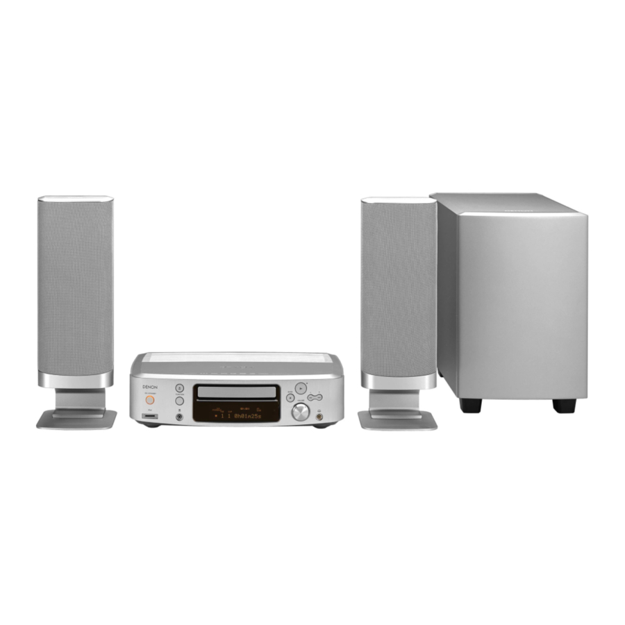
HOME THEATER SYSTEM (S-101) consists of DVD SURROUND RECEIVER (ADV-S101)
and SUB WOOFER (DSW-S101) and SPEAKER SYSTEM (SC-S101)
TE
L 13942296513
For purposes of improvement, specifications and
design are subject to change without notice.
Please use this service manual with referring to the
operating instructions without fail.
Some illustrations using in this service manual are
slightly different from the actual set.
www
.
http://www.xiaoyu163.com
SERVICE MANUAL
MODEL
DVD HOME THEATER SYSTEM
x
ao
u163
y
i
Denon Brand Company, D&M Holdings Inc.
http://www.xiaoyu163.com
2 9
8
S-101
Q Q
3
6 7
1 3
1 5
co
TOKYO, JAPAN
.
9 4
2 8
For U.S.A., Canada
& Europe model
Ver. 1
0 5
8
2 9
9 4
2 8
m
X0244 V.01 DE/CDM 0507
9 9
9 9
Advertisement
Table of Contents

Related Manuals for Denon S-101


Summary of Contents for Denon S-101
- Page 1 SERVICE MANUAL S-101 MODEL DVD HOME THEATER SYSTEM HOME THEATER SYSTEM (S-101) consists of DVD SURROUND RECEIVER (ADV-S101) and SUB WOOFER (DSW-S101) and SPEAKER SYSTEM (SC-S101) L 13942296513 For purposes of improvement, specifications and design are subject to change without notice.
-
Page 2: Safety Precautions
S-101 3 7 63 1515 0 SAFETY PRECAUTIONS The following check should be performed for the continued protection of the customer and service technician. LEAKAGE CURRENT CHECK Before returning the unit to the customer, make sure you make either (1) a leakage current check or (2) a line to chassis resistance check. - Page 3 S-101 RDISASSEMBLY 3 7 63 1515 0 (Follow the procedure below in reverse order when reassembling.) 1. Loader Panel (1) Switch on, and press [ (OPEN/CLOSE)] button to open the Disc tray. (2) Detach the Loader Panel by lifting.
- Page 4 S-101 3. Top Cover 3 7 63 1515 0 (1) Remove 9 top screws, then detach Top Cover. 4. Front Panel Ass’y (1) Remove 3 Front panel screws, then detach P.W.B. and chassis. (2) Remove 4 Front panel side screws, then detach the Front Panel Ass’y.
- Page 5 S-101 Special operating procedures 3 7 63 1515 0 1. Initialization This initializes the data for the function, volume, DVD mechanism (RL-874), etc. (1) Check that the AC cord is disconnected from the power outlet. (AC OFF) (2) While pressing the FUNCTION and OPEN/CLOSE ) buttons on the main unit, plug the AC cord into the power outlet.
- Page 6 S-101 ADJUSTMENT 3 7 63 1515 0 1. SETTING (1) Connect the oscilloscope to the Y-signal, P -signal and -signal, P -signal and C -signal of ZONE2 COMPO- NENT OUT terminal and each terminate at 75 Ohms. Use the 75 Ohms resistance must be 1% (2) DVD test disc : DVDT-S01 (3) S OUT of DVD player is connected to AUX1 S IN.
- Page 7 S-101 3 7 63 1515 0 2.4. Procedure (1) Adjust the signal of COMPONENT OUT by the wave of oscilloscope. (a) Target, Y-signal Point 1U-3695-3 VR601 Adjustment Value 35mV Waveform Y-signal COMPONENT OUT (b) Target, P -signal Point 1U-3695-3 VR602...
- Page 8 S-101 BLOCK DIAGRAM 3 7 6 3 1 5 1 5 0 DATP20:FL/FR DAIP19:C/SW DAIP18:SL/SR DAIP16:FL/FR DAIP16:0/SW DAIP15:0/0 DAIP14:RECL/RECR 1 3 9 4 2 2 9 6 5 1 3 w w w u 1 6 3 http://www.xiaoyu163.com...
- Page 9 S-101 LEVEL DIAGRAM 3 7 63 1515 0 L 13942296513 u163 http://www.xiaoyu163.com...
- Page 10 S-101 3 7 63 1515 0 SEMICONDUCTORS / Only major semiconductors are shown, general semiconductors etc. are omitted to list. 1. IC’s ES6128F (RL-S874: U9) DSCK DSCK AUX[0] AUX[0] AUX[1] AUX[1] DCS0# DCS0# AUX[2] AUX[2] DCS1# DCS1# AUX[3] AUX[3]...
- Page 11 S-101 3 7 63 1515 0 Pin No. Pin Name Function RESET# Reset input, active low. TDMDX TDM transmit data. TDMDR TDM receive data. TDMCLK TDM clock input. TDMFS TDM frame sync. TDMTSC# TDM output enable. Audio transmit frame sync.
- Page 12 S-101 3 7 63 1515 0 Pin No. Pin Name Function Video VDAC output. VDAC YUV7 YUV7 pixel output data. PCLK2XSCN 27 MHz video output pixel clock. PCLKQSCN 13.5 MHz video output pixel clock. VSYNC# Vertical sync, active low.
- Page 13 S-101 3 7 63 1515 0 M5705 (RL-S874: U1) AVSS-DS XRD(3) XSRFIN XRD(12) XSIPIN AVDD5-DS XRD(2) XSDSSLV XRD(13) XSRSLINT XRD(1) XRD(14) XSAWRC XRD(0) XSRFGC XRD(15) XSEFGC XHD(7) XSFOCUS XHD(8) XSTRACK XHD(6) XSSLEG XHD(9) AVDD5-DA XHD(5) XSMOTOR XHD(10) AVSS-DA XHD(4)
- Page 14 S-101 3 7 63 1515 0 Pin No. Pin Name Type Description XSSBAD Sub-beam addition signal input Phase detector reference current generator. Connect a resistor between this pin and XSPDIREF ground to set reference current Frequency detector reference current generator. Connect a resistor between this pin and...
- Page 15 S-101 3 7 63 1515 0 Pin No. Pin Name Type Description XHPDIAGJ This pin is used as the Passed Diagnostics signal, and may be an input or an open-drain output This pin is used as the Drive Active/Slave Present signal, and is an input or an open-drain XHDASPJ output.
- Page 16 S-101 3 7 63 1515 0 M30627FHPGP (IC202: 1U-3694) L 13942296513 Port Port Port Name Explanation Function setting VREF VREF Reference Voltage Input for A/D converter AVcc AVcc Positive power SIN4 FL_CS Chip Enable output to FLD SOUT4 FL_DA...
- Page 17 S-101 3 7 63 1515 0 Port Port Port Name Explanation Function setting NC(L:Output) Not Used: N. C. NC(L:Output) Not Used: N. C. RXD2 NC(L:Output) Not Used: N. C. TXD2 NC(L:Output) Not Used: N. C. TXD1 USB/IPOD_TXD Serial Data output to USB/IPOD...
- Page 18 S-101 3 7 63 1515 0 Port Port Port Name Explanation Function setting /INT3 REMOTE Remote Control signal input Reset output to RDS IC DIR DOUT Serial Data input from DIR. DIR/CODEC DIN Serial Data output to DIR. DIR/CODEC CLK Serial Clock output to DIR.
- Page 19 S-101 3 7 63 1515 0 ADSP-21266SKSTZ-1C (IC906: 1U-3694) PIN 1 INDICATOR TOP VIEW ADSP-21266SKSTZ-1C Terminal Function LQFP LQFP LQFP LQFP Pin Name Pin # Pin Name Pin # Pin Name Pin # Pin Name Pin # DDINT DDINT...
- Page 20 S-101 3 7 63 1515 0 SP3721A (RL-S874: U2) DVDRFP SDEN DVDRFN SDATA SCLK TOP VIEW MEVO MLPF L 13942296513 SP3721A Terminal Function Pin No. Type Description Pin Name 1, 2 DVDREP , DVDREN RF Signal Inputs. Differential RF signal attenuator input pins CDRF RF Signal Inputs.
- Page 21 S-101 3 7 63 1515 0 Pin No. Pin Name Type Description Center Error Signal Output. Center error output reference to VCI NEVO SIGO Bottom Envelope Output. Bottom envelope for mirror detection Defect Output. Pseudo CMOS output. When a defect is detected, the DFT output goes high. Also the servo AGC output can be monitored at this pin, when CAR bits 7-4 are ‘0011’...
- Page 22 S-101 3 7 63 1515 0 TAS5066 (IC805: 1U-3683) 64 63 62 61 60 59 58 57 56 55 54 53 52 51 50 49 DVDD_RCL MCLK_IN DVSS_RCL AVDD_PLL PLL_FLT_OUT DVDD_PWM PLL_FLT_RET DVSS_PWM AVSS_PLL PWM_AP_4 PWM_AM_4 DVSS1 VALID_4 PWM_AP_5...
-
Page 23: Block Diagram
S-101 3 7 63 1515 0 M66005-0001AHP (IC301: 1U-3681) SEG02 SEG19 SEG01 SEG20 SEG21 SEG00 Vcc2 SEG22 SEG23 DIG15/SEG39 SEG24 DIG14/SEG38 DIG13/SEG37 SEG25 SEG26 DIG12/SEG36 M66005-0001AHP DIG11 DIG10 SEG27 DIG09 SEG28 DIG08 SEG29 DIG07 SEG30 SEG31 DIG06 DIG05 SEG32... - Page 24 S-101 3 7 63 1515 0 AD1837 (IC711: 1U-3694) DVDD DVDD DBCLK CLATCH DLRCLK PD/RST AGND AGND OUTR4 TOP VIEW OUTL1 OUTL4 OUTR1 AGND AGND AVDD AVDD OUTR3 OUTL2 DVDD DVDD ODVDD ALRCLK ABCLK ASDATA CCLK CLATCH COUT MCLK...
- Page 25 S-101 3 7 63 1515 0 HY57V651620BTC-75 (RL-S874: U11) DQ 0 DQ15 DQ 1 DQ14 DQ 2 DQ13 DQ 3 DQ12 DQ 4 DQ 11 DQ 5 DQ10 DQ 6 DQ 9 DQ 7 DQ 8 LDQM /W E...
- Page 26 S-101 3 7 63 1515 0 T431616A-8S(RL-S874:U5) DQ15 DQ14 DQ 2 DQ13 DQ 3 DQ12 DQ 4 DQ11 DQ 5 DQ10 DQ 6 DQ 9 DQ 7 DQ 8 LDQM N.C / RFU UD QM CL K CK E...
- Page 27 S-101 3 7 63 1515 0 MX29LV800ABTC-70 (RL-S874: U10) BYTE Q15/A-1 RESET RY/BY BLOCK DIAGRAM WRITE CONTROL PROGRAM/ERASE STATE INPUT HIGH VOLTAGE MACHINE LOGIC RESET (WSM) L 13942296513 STATE REGISTER ADDRESS FLASH ARRAY LATCH ARRAY A0-A19 SOURCE COMMAND DATA...
- Page 28 S-101 3 7 63 1515 0 LC89057W (IC707: 1U-3694) EMPHA/UO AUDIO/VO XMODE RXOUT Microcontroller C bit, U bit 37 DO 36 RERR 24 SDIN 23 SLRCK Input Demodulation 22 SBCK Data Selector 21 RDATA & Selector 21 RDATA Lock Detect...
- Page 29 S-101 3 7 63 1515 0 Pin Name Function XOUT X’tal osc. connecting output terminal X’tal osc. connection, external clock input terminal (24.576MHz or 12.288MHz) DVDD — Digital power DGND — Digital GND EMPHA/UO Emphasis information/U-data output/Chip address setting terminal...
- Page 30 S-101 3 7 63 1515 0 LH28F800BJE (IC907: 1U-3694) CY7C1049CV-33-10ZC (IC908, 910: 1U-3694) Top View INPUT BUFFER L 13942296513 512K x 8 ARRAY POWER COLUMN DOWN DECODER TA1270BF (IC501: 1U-3695) TC90A69F (IC503: 1U-3695) Y OFFSET C BUS PEDESTAL PEDESTAL...
- Page 31 S-101 3 7 63 1515 0 TAS5121 (IC201, 301, 401: 1U-3683) GVDD_B PWM_BP GVDD_B RESET BST_B DREG_RTN PVDD_B GVDD PVDD_B OUT_B DREG OUT_B DGND OUT_A DVDD OUT_A PVDD_A DGND PVDD_A BST_A PWM_AP GVDD_A GVDD_A Terminal Functions TERMINAL FUNCTION (1)
- Page 32 S-101 3 7 63 1515 0 BH7868FS (IC301, 302: 1U-3695) 6MHz Vcc1 COUT S-DCOUT S-DCOUT 6MHz CVOUT Bias CVOUT MUTE1 MUTE1 6MHz CVIN Clamp YOUT SEL (CV/MIX) YOUT SAG Clamp 12MHz BIAS Bias Py/G OUT Py/G OUT SAG SEL (BIAS/CLAMP)
- Page 33 S-101 3 7 63 1515 0 NJM2596 (IC509: 1U-3695) SN74LV573APW (IC903, 904: 1U-3694) L 13942296513 PCM1803 (IC803, 804: 1U-3683) MODE1 MODE0 FMT1 FMT0 AGND SCKI PDWN BYPAS DGND TEST DOUT LRCK BLOCK DIAGRAM DeltaœSigma Modulator LRCK DOUT Serial ψ1/64 , ψ1/128...
- Page 34 S-101 3 7 63 1515 0 QT240 (IC306: 1U-3681) 1-1 P - QT240-ISS ABLE ISTING Name Description SNS2 Sense pin (to Rs2 + Cs2) SNS2K Sense pin (to Cs2, electrode) SNS2 SNS3K SNS1 Sense pin (to Rs1 + Cs1)
- Page 35 S-101 3 7 63 1515 0 BU4053BCF (IC510: 1U-3695) BU4052BCF (IC518: 1U-3695) YOUT COMMON Y XOUT COMMON X TC74VHC74FT (IC703: 1U-3694) NJM2274R (IC502: 1U-3695) VIEW Power Save CTL Vref Clamp Disc. Bias C Mute CTL BR93L86RFVM-WTR (IC201: 1U-3694) DE T E C T...
- Page 36 S-101 3 7 63 1515 0 BD9781HFP (IC810: 1U-3695) EN/SYNC 5~35V ON/OFF L:OFF H:ON 220 F Vref SYNC SOFT START B D 9 7 8 1 H V F P ERROR AMP COMPARATOR DRIVER LATCH 33 H 150K RESET...
- Page 37 S-101 3 7 63 1515 0 STR-F6238S (IC902: 1U-3682: E3) STR-F6267S (IC902: 1U-3682: E2) DR V .R E G O.V .P Latch S tart R g2 R g3 R g1 R eg. FRONT DR V VIEW T .S .D.
- Page 38 S-101 3 7 63 1515 0 NJM7912FA (IC807: 1U-3695) (IC905: 1U-3682) SE-B2 (IC908: 1U-3682) FRONT FRONT VIEW VIEW 1 REF NJM78L07UA (IC512: 1U-3694) NJM79L07AU (IC513: 1U-3694) COMMON NJM7805FA (IC712: 1U-3694) (IC801: 1U-3695) NJM7812FA (IC806: 1U-3695) (IC909: 1U-3682) BA033T (IC904: 1U-3682) BA05T (IC907: 1U-3682) LM2990T-5.0 (IC809: 1U-3695)
- Page 39 S-101 2. FL DISPLAY 3 7 63 1515 0 15-BT-102GN Pin Connection Grid Assigment L 13942296513 Anode Connection u163 http://www.xiaoyu163.com...
- Page 40 S-101 PRINTED WIRING BOARDS 3 7 6 3 1 5 1 5 0 1U-3694 MAIN P.W.B. UNIT 1 3 9 4 2 2 9 6 5 1 3 w w w u 1 6 3 COMPONENT SIDE http://www.xiaoyu163.com...
- Page 41 S-101 3 7 6 3 1 5 1 5 0 1 3 9 4 2 2 9 6 5 1 3 w w w u 1 6 3 FOIL SIDE http://www.xiaoyu163.com...
- Page 42 S-101 3 7 6 3 1 5 1 5 0 1U-3695 I/F P.W.B. UNIT 1 3 9 4 2 2 9 6 5 1 3 w w w u 1 6 3 COMPONENT SIDE http://www.xiaoyu163.com...
- Page 43 S-101 3 7 6 3 1 5 1 5 0 1 3 9 4 2 2 9 6 5 1 3 w w w u 1 6 3 FOIL SIDE http://www.xiaoyu163.com...
- Page 44 S-101 3 7 6 3 1 5 1 5 0 1U-3681 DISPLAY P.W.B. UNIT 1 3 9 4 2 2 9 6 5 1 3 w w w u 1 6 3 COMPONENT SIDE http://www.xiaoyu163.com...
- Page 45 S-101 3 7 6 3 1 5 1 5 0 1 3 9 4 2 2 9 6 5 1 3 w w w u 1 6 3 FOIL SIDE http://www.xiaoyu163.com...
- Page 46 S-101 3 7 6 3 1 5 1 5 0 1U-3682 SMPS P.W.B. UNIT 1 3 9 4 2 2 9 6 5 1 3 w w w u 1 6 3 COMPONENT SIDE http://www.xiaoyu163.com...
- Page 47 S-101 3 7 6 3 1 5 1 5 0 1 3 9 4 2 2 9 6 5 1 3 w w w u 1 6 3 FOIL SIDE http://www.xiaoyu163.com...
- Page 48 S-101 3 7 6 3 1 5 1 5 0 1U-3683 AMP P.W.B. UNIT 1 3 9 4 2 2 9 6 5 1 3 w w w u 1 6 3 COMPONENT SIDE http://www.xiaoyu163.com...
- Page 49 S-101 3 7 6 3 1 5 1 5 0 1 3 9 4 2 2 9 6 5 1 3 w w w u 1 6 3 FOIL SIDE http://www.xiaoyu163.com...
- Page 50 S-101 3 7 6 3 1 5 1 5 0 MECHANISM P.W.B. UNIT 1 3 9 4 2 2 9 6 5 1 3 COMPONENT SIDE FOIL SIDE w w w u 1 6 3 http://www.xiaoyu163.com...
- Page 51 S-101 NOTE FOR PARTS LIST 3 7 63 1515 0 • Part indicated with the mark "nsp" are not always in stock and possibly to take a long period of time for supplying, or in some case supplying of part may be refused.
- Page 52 S-101 PARTS LIST OF P.W.B. UNIT 3 7 63 1515 0 The parts listed below are for maintenance only, might differ from the parts used in the unit in appearances or dimensions. Part indicated with the mark “nsp” are not always in stock and possibly to take a long period of time for supplying, or in some case supplying of part may be refused.
- Page 53 S-101 3 7 63 1515 0 Ref. No. Part No. Part Name Remarks Q'ty New TR213 00D 269 0192 902 KRC102S-RTK(10K-10K) +C TR501,502 00D 275 0100 902 2SK771-5-TB TR503 00D 273 0485 906 KRC107S-RTK(10K-47K) TR504 00D 269 0184 907...
- Page 54 S-101 3 7 63 1515 0 Ref. No. Part No. Part Name Remarks Q'ty New CAPACITORS GROUP C101,102 00D 257 0501 901 CK73B1H103KT (1608) +1608 C117 00D 257 0509 929 CK73B1H102KT +1608 C118 00D 257 0511 904 CK73F1H103ZT +1608...
- Page 55 S-101 3 7 63 1515 0 Ref. No. Part No. Part Name Remarks Q'ty New C226 00D 257 0512 903 CK73F1E104ZT +1608 C227,228 00D 257 0506 951 CC73CH1H101JT +1608 C229 00D 254 4740 921 CE67W1C470MT(GV) C230 00D 257 0512 903...
- Page 56 S-101 3 7 63 1515 0 Ref. No. Part No. Part Name Remarks Q'ty New C315-318 00D 256 1058 939 CF93A1H473JT (JL) C319,320 00D 257 0511 917 CK73F1H223ZT +1608 C321,322 00D 254 4742 916 CE67W1V100MT(GV) C401-408 00D 257 0507 934...
- Page 57 S-101 3 7 63 1515 0 Ref. No. Part No. Part Name Remarks Q'ty New C615 00D 257 0501 901 CK73B1H103KT (1608) +1608 C616 00D 254 3088 901 CE67W1C220MBPT(RV) C617 00D 257 0503 925 CC73CH1H100DT +1608 C618 00D 257 0511 917...
- Page 58 S-101 3 7 63 1515 0 Ref. No. Part No. Part Name Remarks Q'ty New C741 00D 257 0512 903 CK73F1E104ZT +1608 C742 00D 257 0511 904 CK73F1H103ZT +1608 C743 00D 254 4740 976 CE67W1C100MT(GV) C744 00D 254 4742 916...
- Page 59 S-101 3 7 63 1515 0 Ref. No. Part No. Part Name Remarks Q'ty New C903 00D 254 4720 941 CE04W1E470MT(GR) C910 00D 257 0516 954 CK73B1E104KT +1608 C911 00D 257 0509 929 CK73B1H102KT +1608 C912 00D 257 0516 954...
- Page 60 S-101 3 7 63 1515 0 Ref. No. Part No. Part Name Remarks Q'ty New CX211 00D 205 1006 022 21P FFC BASE (P=1) CY091 00D 205 1100 025 9P FFC BASE(P=1) CY151 00D 205 0736 076 15P FFC CON.BASE...
- Page 61 S-101 00D1U-3695D I/F P.W.B. UNIT ASS'Y (for U.S.A. & Canada model) 3 7 63 1515 0 Ref. No. Part No. Part Name Remarks Q'ty New SEMICONDUCTORS GROUP IC170 00D 263 0896 909 NJM2068MD-TE1 IC301 00D 262 3365 900 BH7868FS...
- Page 62 S-101 3 7 63 1515 0 Ref. No. Part No. Part Name Remarks Q'ty New D815 00D 276 0401 905 1SS133T77 (TAPE) D816 00D 276 0773 905 RB501V-40 +2125 D817 00D 276 0827 903 SPB-G54SVR D818 00D 276 0825 905...
- Page 63 S-101 3 7 63 1515 0 Ref. No. Part No. Part Name Remarks Q'ty New C527 00D 257 0516 954 CK73B1E104KT +1608 C528 00D 254 4718 908 CE04W1C100MT(GR) C529 00D 254 4722 981 CE04W1H100MT(GR) C530 00D 254 4737 947...
- Page 64 S-101 3 7 63 1515 0 Ref. No. Part No. Part Name Remarks Q'ty New C609 00D 257 0503 941 CC73CH1H120JT +1608 C610 00D 257 0516 954 CK73B1E104KT +1608 C611,612 00D 257 0501 901 CK73B1H103KT (1608) +1608 C613 00D 254 4734 924...
- Page 65 S-101 3 7 63 1515 0 Ref. No. Part No. Part Name Remarks Q'ty New C839 00D 257 0512 903 CK73F1E104ZT +1608 C840,841 00D 257 0511 904 CK73F1H103ZT +1608 C842 00D 257 0512 903 CK73F1E104ZT +1608 C843,844 00D 254 4716 926...
- Page 66 S-101 3 7 63 1515 0 Ref. No. Part No. Part Name Remarks Q'ty New CY161,162 00D 205 1326 061 16P SOCKT(9120) CY173 00D 205 1352 035 17P-FFC-BASE(TOC-J) CY201,202 00D 205 1354 004 20P SOCKT(9120) CY251 00D 205 1355 003...
- Page 67 S-101 00D1U-3695E I/F P.W.B. UNIT ASS'Y (for Europe model) 3 7 63 1515 0 Ref. No. Part No. Part Name Remarks Q'ty New SEMICONDUCTORS GROUP IC170 00D 263 0896 909 NJM2068MD-TE1 IC301,302 00D 262 3365 900 BH7868FS IC304 00D 262 2745 903...
- Page 68 S-101 3 7 63 1515 0 Ref. No. Part No. Part Name Remarks Q'ty New D801 00D 276 0401 905 1SS133T77 (TAPE) D802 00D 276 0824 906 SFPB-64V D805-812 00D 276 0780 901 SFPX-62 D813 00D 276 0401 905...
- Page 69 S-101 3 7 63 1515 0 Ref. No. Part No. Part Name Remarks Q'ty New C359 00D 254 4718 911 CE04W1C220MT(GR) C360 00D 257 0512 903 CK73F1E104ZT +1608 C361-363 00D 257 0504 982 CC73CH1H470JT +1608 C367 00D 254 4722 907...
- Page 70 S-101 3 7 63 1515 0 Ref. No. Part No. Part Name Remarks Q'ty New C596 00D 254 4722 952 CE04W1H2R2MT(GR) C597,598 00D 254 4732 942 CE04W0J101MT(SF) C599,600 00D 257 0516 954 CK73B1E104KT +1608 C601 00D 254 4722 952...
- Page 71 S-101 3 7 63 1515 0 Ref. No. Part No. Part Name Remarks Q'ty New C817 00D 257 1020 902 CK73B1H105KT C819 00D 254 4709 700 CE04W1V221MC JC5(KY) C820 00D 254 4708 701 CE04W1V471MC J20(KY) C822 00D 255 1280 908...
- Page 72 S-101 3 7 63 1515 0 Ref. No. Part No. Part Name Remarks Q'ty New CX065 00D 205 1072 946 6P PH CON.BASE +REF CX091 00D 205 1100 025 9P FFC BASE(P=1) CX101 00D 205 0375 000 10P CON.BASE(KR-PH)
- Page 73 S-101 3 7 63 1515 0 Ref. No. Part No. Part Name Remarks Q'ty New W802 LUG PLATE X501 00D 399 0810 006 CSB503F30 X502 00D 399 0802 001 XTAL(3.58MHZ) X503 00D 399 0809 004 XTAL(4.43MHZ) INSULATING SHEET 220...
- Page 74 S-101 00D1U-3681D DISPLAY P.W.B. UNIT ASS'Y 3 7 63 1515 0 Ref. No. Part No. Part Name Remarks Q'ty New SEMICONDUCTORS GROUP IC301 00D 262 3512 009 M66005-0001AHP IC302 00D 499 0306 001 GP1UE271XK IC303 00D 262 2745 903...
- Page 75 S-101 3 7 63 1515 0 Ref. No. Part No. Part Name Remarks Q'ty New C331 00D 254 4734 911 CE04W1C100MT(SF) C332 00D 257 0509 929 CK73B1H102KT +1608 C333,334 00D 257 0501 901 CK73B1H103KT (1608) +1608 C336 00D 257 0509 929...
- Page 76 S-101 3 7 63 1515 0 Ref. No. Part No. Part Name Remarks Q'ty New JK301 00D 204 8636 010 MINI JACK(ST SW) JK303 00D 204 8636 010 MINI JACK(ST SW) S301-305 00D 212 0467 000 TACT SW(H=5) S306...
- Page 77 S-101 00D1U-3682D SMPS P.W.B. UNIT ASS'Y (for U.S.A. & Canada model) 3 7 63 1515 0 Ref. No. Part No. Part Name Remarks Q'ty New SEMICONDUCTORS GROUP IC901 00D 262 3509 708 SI-8120E (LF1101) IC902 00D 265 0116 009...
- Page 78 S-101 3 7 63 1515 0 Ref. No. Part No. Part Name Remarks Q'ty New C907-909 00D 253 8022 710 CK45F2EAC222MC C910,911 00D 256 8038 004 CF99--2EAC104M C912 00D 253 8022 710 CK45F2EAC222MC C913 00D 255 4261 775 CQ93P2J392KC(ECQP)
- Page 79 S-101 3 7 63 1515 0 Ref. No. Part No. Part Name Remarks Q'ty New F901 00D 206 1094 066 FUSE(233)T4AL125V F902 00D 206 1094 037 FUSE(233)T2AL125V FF901,902 00D 202 0040 909 FUSE CLIP(TAPE) FH901,902 00D 202 0040 909...
- Page 80 S-101 00D1U-3682E SMPS P.W.B. UNIT ASS'Y (for Europe model) 3 7 63 1515 0 Ref. No. Part No. Part Name Remarks Q'ty New SEMICONDUCTORS GROUP IC901 00D 262 3509 708 SI-8120E (LF1101) IC902 00D 265 0118 007 STR-F6267S(LF1351) IC903...
- Page 81 S-101 3 7 63 1515 0 Ref. No. Part No. Part Name Remarks Q'ty New C907,908 00D 253 8022 710 CK45F2EAC222MC C909 00D 253 8022 723 CK45F2EAC102MC C910,911 00D 256 8038 004 CF99--2EAC104M C912 00D 253 8022 723 CK45F2EAC102MC...
- Page 82 S-101 3 7 63 1515 0 Ref. No. Part No. Part Name Remarks Q'ty New CY071 00D 205 0233 074 7P EH CONNECTOR BASE CY101 00D 205 0275 003 10P EH CON. BASE F901 00D 206 1096 035 FUSE(218)T2.5AL250V...
- Page 83 S-101 00D1U-3683D AMP P.W.B. UNIT ASS'Y 3 7 63 1515 0 Ref. No. Part No. Part Name Remarks Q'ty New SEMICONDUCTORS GROUP IC201 00D 262 3503 908 TAS5121DKDR IC301 00D 262 3503 908 TAS5121DKDR IC401 00D 262 3503 908...
- Page 84 S-101 3 7 63 1515 0 Ref. No. Part No. Part Name Remarks Q'ty New C216,217 00D 257 0516 954 CK73B1E104KT +1608 C218 00D 253 1180 921 CK45B1H102KT(DD-3) C301-303 00D 257 0035 901 CK73B1H104KT +2125 C305 00D 257 0024 909...
- Page 85 S-101 3 7 63 1515 0 Ref. No. Part No. Part Name Remarks Q'ty New C576 00D 257 0511 904 CK73F1H103ZT +1608 C577 00D 257 0509 929 CK73B1H102KT +1608 C578 00D 257 0511 904 CK73F1H103ZT +1608 C579 00D 257 0509 929...
- Page 86 S-101 3 7 63 1515 0 Ref. No. Part No. Part Name Remarks Q'ty New OTHERS PARTS GROUP CX022 00D 205 0581 069 2P VH-VH CON BASE CX031 00D 205 0233 032 3P EH CONNECTOR BASE CX041,042 00D 205 0653 049 4P VH CON.BASE...
- Page 87 S-101 MECHANISM P.W.B. UNIT ASS'Y 3 7 63 1515 0 Ref. No. Part No. Part Name Remarks Q'ty New SEMICONDUCTORS GROUP 00D 943 0011 903 M5705 00D 943 0012 009 SP3721A 00D 943 0012 805 AT49F001N-70JC 00D 943 0012 902...
- Page 88 S-101 3 7 63 1515 0 Ref. No. Part No. Part Name Remarks Q'ty New CAPACITORS GROUP 00D 943 0015 226 CERAMIC,0.047U (47N),10%,16V 00D 943 0015 174 CERAMIC,560P,10%,50V C4,5 00D 943 0015 255 CERAMIC,0.1U,-20 - 80%,25V 00D 943 0015 132...
- Page 89 S-101 3 7 63 1515 0 Ref. No. Part No. Part Name Remarks Q'ty New 00D 943 0015 271 ELECTROLYTIC,20%,22U/6.3V 00D 943 0015 310 ELECTROLYTIC,20%,220U/6.3V 00D 943 0015 297 ELECTROLYTIC,20%,100U/6.3V TC11,12 00D 943 0015 297 ELECTROLYTIC,20%,100U/6.3V TC13 00D 943 0015 310 ELECTROLYTIC,20%,220U/6.3V...
- Page 90 S-101 EXPLODED VIEW 3 7 6 3 1 5 1 5 0 E2 oniy 1 3 9 4 2 2 9 6 5 1 3 WARNING: Parts marked with this symbol have critical characteristics. Use ONLY replacement parts recommended by the manufacturer.
- Page 91 S-101 PARTS LIST OF EXPLODED VIEW 3 7 63 1515 0 The parts listed below are for maintenance only, might differ from the parts used in the unit in appearances or dimensions. Part indicated with the mark “nsp” are not always in stock and possibly to take a long period of time for supplying, or in some case supplying of part may be refused.
- Page 92 S-101 3 7 63 1515 0 Ref. No. Part No. Part Name Remarks Q'ty New 00D 461 1168 036 RUBBER SHEET 00D 146 2414 233 TOP COVER for E2 00D 146 2414 217 TOP COVER for E3 00D 102 0685 006...
- Page 93 S-101 3 7 63 1515 0 Ref. No. Part No. Part Name Remarks Q'ty New SCREWS 00D 473 8089 001 3X15 CUP SCREW 00D 475 6006 008 00D 473 7015 005 3X6 CBTS(S)-B 00D 473 7005 073 3X5 CBTS(S)Z 00D 473 7001 048 2.6X8 CBTS (S)-Z...
- Page 94 S-101 EXPLODED VIEW OF DVD MECHANISM UNIT 3 7 63 1515 0 L 13942296513 PARTS LIST OF DVD MECHANISM UNIT The parts listed below are for maintenance only, might differ from the parts used in the unit in appearances or dimensions.
- Page 95 S-101 3 7 63 1515 0 Ref. No. Part No. Part Name Remarks Q'ty New 00D 943 0009 708 BELT 00D 943 0009 300 AY L/MOTOR 00D 943 0009 407 SLIDE, CAM 00D 943 0009 601 GEAR, PULLY 00D 943 0009 805...
- Page 96 S-101 DSW-S101 EXPLODED VIEW 3 7 6 3 1 5 1 5 0 1 3 9 4 2 2 9 6 5 1 3 WARNING: Parts marked with this symbol have critical characteristics. Use ONLY replacement parts recommended by w w w the manufacturer.
- Page 97 S-101 DSW-S101 PARTS LIST OF EXPLODED VIEW 3 7 63 1515 0 The parts listed below are for maintenance only, might differ from the parts used in the unit in appearances or dimensions. Part indicated with the mark “nsp” are not always in stock and possibly to take a long period of time for supplying, or in some case supplying of part may be refused.
- Page 98 S-101 3 7 63 1515 0 Ref. No. Part No. Part Name Remarks Q'ty New 00D 513 4093 001 DANGEROUS LABEL 00D 203 6629 000 4P EH-EH CON.CORD 00D 204 2993 005 7P EH-EH CON.CORD 00D 204 2994 004 10P EH-EH CON.CORD...
- Page 99 S-101 SC-S101 EXPLODED VIEW 3 7 63 1515 0 for Lch for Rch L 13942296513 SC-S101 PARTS LIST OF EXPLODED VIEW The parts listed below are for maintenance only, might differ from the parts used in the unit in appearances or dimensions.
- Page 100 S-101 3 7 63 1515 0 Ref. No. Part No. Part Name Remarks Q'ty PACKING E 29-000-349-01 00D 949 0057 402 CABINET R ch CABINET 52-000-182-01 PACKING C 29-000-347-01 PACKING D 29-000-348-01 SOUND ABSORBENT 54-000-152-01 SOUND ABSORBENT 54-000-152-11 INSERT NUTS...
- Page 101 S-101 PACKING VIEW 3 7 63 1515 0 DVD SURROUNDRECIEVER ADV-S101 ACCESSORY BOX ASSY SPEAKER SYSTEM SCS101SRM 102 105 SUB WOOFER 106 107 108 L 13942296513 MASTER CARTON PARTS LIST OF PACKING & ACCESSORIES The parts listed below are for maintenance only, might differ from the parts used in the unit in appearances or dimensions.
- Page 102 S-101 3 7 63 1515 0 Ref. No. Part No. Part Name Remarks Q'ty 00D 503 1511 107 CUSHION (L) for ADV-S101 00D 503 1512 106 CUSHION (R) for ADV-S101 00D 501 2304 003 ACCESSARY BOX for E3 00D 501 2304 016...
- Page 103 S-101 WIRONG DIAGRAM 3 7 63 1515 0 (1) S101 DSW-S101 SC-S101 SC-S101 ADV-S101 ITEM PART NO. PART NAME 00D 204 6794 006 25P D-SUB CABLE 00D 203 2439 003 SP CABLE ASSY (2) DSW-S101 ADV-S101 CX251 TERMINAL UNIT...
- Page 104 S-101 3 7 63 1515 0 (2) ADV-S101 DSW-S101 CY251 LOCAL POWER UNIT TUNER 1U-3695D-1(E3) PACK 1U-3695E-1(E2) CONVERT UNIT CY072(E2) CX162 CX141 CX162 1U-3695D-3(E3) 1U-3695E-3(E2) (Board to (Board to (Board to CX051(E3) Board) Board) Board) I/F BOARD UNIT 1U-3695D-2(E3)
- Page 105 S-101 3 7 63 1515 0 ITEM PART NO. PART NAME 00D 203 5372 002 3P ZH-PH CON.CORD 00D 204 0599 003 6P PH-PH CON.CORD E2 ONLY 00D 204 8567 005 5P PH-PH CON.CORD E3 ONLY 00D 009 0265 004...
- Page 106 S-101 NOTE FOR SCHEMATIC DIAGRAM 3 7 63 1515 0 WARNING: Parts marked with this symbol ! have critical characteristics. Use ONLY replacement parts recommended by the manufactur- CAUTION: Before returning the unit to the customer, make sure you make µ...
- Page 107 S-101 SCHEMATIC DIAGRAMS (1/26) 3 7 6 3 1 5 1 5 0 1 3 9 4 2 2 9 6 5 1 3 w w w u 1 6 3 SIGNAL LINE SCHEMATIC DIAGRAMS (1/26) MAIN UNIT (1/5)
- Page 108 S-101 SCHEMATIC DIAGRAMS (2/26) 3 7 6 3 1 5 1 5 0 1 3 9 4 2 2 9 6 5 1 3 w w w u 1 6 3 SIGNAL LINE SCHEMATIC DIAGRAMS (2/26) MAIN UNIT (2/5)
- Page 109 S-101 SCHEMATIC DIAGRAMS (3/26) 3 7 6 3 1 5 1 5 0 1 3 9 4 2 2 9 6 5 1 3 w w w u 1 6 3 SIGNAL LINE SCHEMATIC DIAGRAMS (3/26) MAIN UNIT (3/5)
- Page 110 S-101 SCHEMATIC DIAGRAMS (4/26) 3 7 6 3 1 5 1 5 0 1 3 9 4 2 2 9 6 5 1 3 w w w u 1 6 3 SIGNAL LINE SCHEMATIC DIAGRAMS (4/26) MAIN UNIT (4/5)
- Page 111 S-101 SCHEMATIC DIAGRAMS (5/26) 3 7 6 3 1 5 1 5 0 1 3 9 4 2 2 9 6 5 1 3 w w w u 1 6 3 SIGNAL LINE SCHEMATIC DIAGRAMS (5/26) MAIN UNIT (5/5)
- Page 112 S-101 SCHEMATIC DIAGRAMS (6/26) 3 7 6 3 1 5 1 5 0 1 3 9 4 2 2 9 6 5 1 3 w w w u 1 6 3 SCHEMATIC DIAGRAMS (6/26) 1U-3695-4 VIDEO I/O UNIT (E3 model only)
- Page 113 S-101 SCHEMATIC DIAGRAMS (7/26) 3 7 6 3 1 5 1 5 0 1 3 9 4 2 2 9 6 5 1 3 w w w u 1 6 3 SCHEMATIC DIAGRAMS (7/26) 1U-3695-4 VIDEO I/O UNIT (E2 model only)
- Page 114 S-101 SCHEMATIC DIAGRAMS (8/26) 3 7 6 3 1 5 1 5 0 1 3 9 4 2 2 9 6 5 1 3 w w w u 1 6 3 SCHEMATIC DIAGRAMS (8/26) 1U-3695-3 CONVERT UNIT (1/2) (E3 model only)
- Page 115 S-101 SCHEMATIC DIAGRAMS (9/26) 3 7 6 3 1 5 1 5 0 1 3 9 4 2 2 9 6 5 1 3 w w w u 1 6 3 SCHEMATIC DIAGRAMS (9/26) 1U-3695-3 CONVERT UNIT (1/2) (E2 model only)
- Page 116 S-101 SCHEMATIC DIAGRAMS (10/26) 3 7 6 3 1 5 1 5 0 1 3 9 4 2 2 9 6 5 1 3 w w w u 1 6 3 SCHEMATIC DIAGRAMS (10/26) 1U-3695-3 CONVERT UNIT (2/2) (E3 model only)
- Page 117 S-101 SCHEMATIC DIAGRAMS (11/26) 3 7 6 3 1 5 1 5 0 1 3 9 4 2 2 9 6 5 1 3 w w w u 1 6 3 SIGNAL LINE SCHEMATIC DIAGRAMS (11/26) 1U-3695-3 CONVERT UNIT (2/2) (E2 model only) http://www.xiaoyu163.com...
- Page 118 S-101 SCHEMATIC DIAGRAMS (12/26) 3 7 6 3 1 5 1 5 0 1 3 9 4 2 2 9 6 5 1 3 w w w u 1 6 3 SIGNAL LINE SCHEMATIC DIAGRAMS (12/26) 1U-3695-1 LOCAL POWER UNIT...
- Page 119 S-101 SCHEMATIC DIAGRAMS (13/26) 3 7 6 3 1 5 1 5 0 1 3 9 4 2 2 9 6 5 1 3 w w w u 1 6 3 SIGNAL LINE SCHEMATIC DIAGRAMS (13/26) 1U-3695-2 I/F BOARD UNIT...
- Page 120 S-101 SCHEMATIC DIAGRAMS (14/26) 3 7 6 3 1 5 1 5 0 1 3 9 4 2 2 9 6 5 1 3 w w w SIGNAL LINE u 1 6 3 SCHEMATIC DIAGRAMS (14/26) 1U-3681-1 DISPLAY CENTER UNIT...
- Page 121 S-101 SCHEMATIC DIAGRAMS (15/26) 3 7 6 3 1 5 1 5 0 1 3 9 4 2 2 9 6 5 1 3 w w w u 1 6 3 SIGNAL LINE SCHEMATIC DIAGRAMS (15/26) 1U-3681-11 iPOD in UNIT...
- Page 122 S-101 SCHEMATIC DIAGRAMS (16/26) 3 7 6 3 1 5 1 5 0 1 3 9 4 2 2 9 6 5 1 3 w w w u 1 6 3 SIGNAL LINE SCHEMATIC DIAGRAMS (16/26) 1U-3683D-2 IN/OUT UNIT 1U-3683D-3 TERMINAL UNIT http://www.xiaoyu163.com...
- Page 123 S-101 SCHEMATIC DIAGRAMS (17/26) 3 7 6 3 1 5 1 5 0 1 3 9 4 2 2 9 6 5 1 3 w w w u 1 6 3 SIGNAL LINE SCHEMATIC DIAGRAMS (17/26) 1U-3683D-1 AMP UNIT (1/2)
- Page 124 S-101 SCHEMATIC DIAGRAMS (18/26) 3 7 6 3 1 5 1 5 0 1 3 9 4 2 2 9 6 5 1 3 w w w u 1 6 3 SIGNAL LINE SCHEMATIC DIAGRAMS (18/26) 1U-3683D-1 AMP UNIT (2/2)
- Page 125 S-101 SCHEMATIC DIAGRAMS (19/26) 3 7 6 3 1 5 1 5 0 1 3 9 4 2 2 9 6 5 1 3 w w w u 1 6 3 SCHEMATIC DIAGRAMS (19/26) 1U-3682-1 SMPS UNIT (E3 model only)
- Page 126 S-101 SCHEMATIC DIAGRAMS (20/26) 3 7 6 3 1 5 1 5 0 1 3 9 4 2 2 9 6 5 1 3 w w w u 1 6 3 SCHEMATIC DIAGRAMS (20/26) 1U-3682-1 SMPS UNIT (E2 model only)
- Page 127 S-101 SCHEMATIC DIAGRAMS (21/26) 3 7 6 3 1 5 1 5 0 1 3 9 4 2 2 9 6 5 1 3 w w w u 1 6 3 SIGNAL LINE SCHEMATIC DIAGRAMS (21/26) ES6028 RC1117-285T Open 4.7Kohm...
- Page 128 S-101 SCHEMATIC DIAGRAMS (22/26) 3 7 6 3 1 5 1 5 0 CS4392 OPEN 1 3 9 4 2 2 9 6 5 1 3 w w w u 1 6 3 SIGNAL LINE SCHEMATIC DIAGRAMS (22/26) MECHANISM BOARD (2/6) AUDIO_DAC http://www.xiaoyu163.com...
- Page 129 S-101 SCHEMATIC DIAGRAMS (23/26) 3 7 6 3 1 5 1 5 0 1 3 9 4 2 2 9 6 5 1 3 w w w u 1 6 3 SCHEMATIC DIAGRAMS (23/26) MECHANISM BOARD (3/6) DRIVE_IC http://www.xiaoyu163.com...
- Page 130 S-101 SCHEMATIC DIAGRAMS (24/26) 3 7 6 3 1 5 1 5 0 DVD-310 : OPEN 1 3 9 4 2 2 9 6 5 1 3 w w w u 1 6 3 SCHEMATIC DIAGRAMS (24/26) MECHANISM BOARD (4/6) DRAM_FE http://www.xiaoyu163.com...
- Page 131 S-101 SCHEMATIC DIAGRAMS (25/26) 3 7 6 3 1 5 1 5 0 1 3 9 4 2 2 9 6 5 1 3 w w w u 1 6 3 SIGNAL LINE SCHEMATIC DIAGRAMS (25/26) MECHANISM BOARD (5/6) RF_AMP http://www.xiaoyu163.com...
- Page 132 S-101 SCHEMATIC DIAGRAMS (26/26) 3 7 6 3 1 5 1 5 0 1 3 9 4 2 2 9 6 5 1 3 w w w u 1 6 3 SIGNAL LINE SCHEMATIC DIAGRAMS (26/26) MECHANISM BOARD (6/6) DVD_DSP http://www.xiaoyu163.com...
- Page 133 S-101 DOCUMENTS FOR WEEE 3 7 63 1515 0 Details of Recycle Parts You have to remove the parts that marked “WEEE Mark " when the recycling processing. (Europe model only) Recycle Parts for ADV-S101 WEEE Ref. No. Part Name...
- Page 134 S-101 3 7 63 1515 0 WEEE Ref. No. Part Name Material Q'ty Mark 17P FFC CABLE Complex 21P FFC CABLE Complex 14P FFC CABLE(AD) Complex 3X15 CUP SCREW STEEL STEEL 3X6 CBTS(S)-B STEEL 3X5 CBTS(S)Z STEEL 2.6X8 CBTS (S)-Z...
- Page 135 S-101 3 7 63 1515 0 WEEE Ref. No. Part Name Material Q'ty Mark 4P VH-VH CON.CORD Complex 11P EH-EH CON.CORD Complex 15P PH-PH CON.CORD Complex 4X30 CBTS(1) BK STEEL 3X6 CBTS(S)-Z STEEL 3X8 CFTS (S)-B STEEL 3X10 CBTS (S)-Z...
- Page 136 S-101 3 7 6 3 1 5 1 5 0 Exploded view of ADV-S101 You have to remove the parts that marked "WEEE mark " when the recycling processing. (Europe model only) 1 3 9 4 2 2 9 6 5 1 3...
- Page 137 S-101 3 7 6 3 1 5 1 5 0 Exploded view of DSW-S101 You have to remove the parts that marked "WEEE mark " when the recycling processing. (Europe model only) 1 3 9 4 2 2 9 6 5 1 3...
- Page 138 S-101 3 7 6 3 1 5 1 5 0 Exploded view of SC-S101 You have to remove the parts that marked "WEEE mark " when the recycling processing. (Europe model only) 1 3 9 4 2 2 9 6 5 1 3...
- Page 139 S-101 3 7 63 1515 0 Details of Recycle parts for Power transformer Part No.37 : POWER TRANS Material STEEL STEEL COPPER WIRE COPPER WIRE COPPER COPPER L 13942296513 Part No.38 : POWER TRANS Material STEEL COPPER COPPER COPPER u163 http://www.xiaoyu163.com...
Need help?
Do you have a question about the S-101 and is the answer not in the manual?
Questions and answers