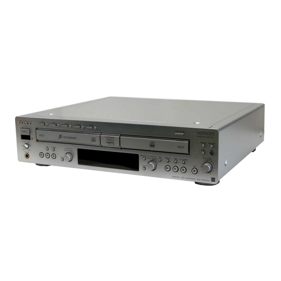
Sony RCD-W2000ES Sevice Manual
Compact disc recorder
Hide thumbs
Also See for RCD-W2000ES:
- Operating instructions manual (44 pages) ,
- Limited warranty (1 page)
Table of Contents
Advertisement
SERVICE MANUAL
Ver 1.1 2003. 12
DECK A (the CD player section)
System
Compact disc digital audio system
Laser
Semiconductor laser
(λ = 780 nm)
Emission duration: continuous
Playable discs
CD, CD-R, CD-RW
Frequency response
20 Hz – 20,000 Hz (±0.5 dB)
Signal to Noise Ratio
Over 100 dB during play
Wow and flutter
Below measurable limit
DECK B (the CD-R and CD-RW recording section)
System
Compact disc digital audio system
Laser
Semiconductor laser
(λ = 780 nm)
Emission duration: continuous
Playable discs
CD, CD-R, CD-RW
Recordable discs
CD-R, CD-RW (for Audio)
Frequency response
20 Hz - 20,000 Hz (±0.5 dB)
Signal to Noise Ratio
Over 100 dB during play
Wow and flutter
Below measurable limit
Inputs
ANALOG IN
Impedance : 47 kilohms
(Phono jacks)
Rated input: 500 mVrms
Minimum input: 250 mVrms
DIGITAL OPTICAL IN
(Square optical connector jack) Optical wavelength: 660 nm
DIGITAL COAXIAL IN
(Phono jack)
Impedance: 75 ohms
Rated output: 0.5 Vp-p, ±20 %
Sony Corporation
9-961-002-02
2003L02-1
Home Audio Company
© 2003.12
Published by Sony Engineering Corporation
RCD-W2000ES
Model Name Using Similar Mechanism
CD Mechanism Type
CD Section
Base Unit Type
Optical Pick-up Type
Model Name Using Similar Mechanism
CD-R/CD-RW CD Mechanism Type
Section
Base Unit Type
Optical Pick-up Type
SPECIFICATIONS
Outputs
ANALOG OUT 1, OUT 2
(Phono jacks)
DIGITAL OPTICAL OUT 1, OUT 2
(Square optical connector jack) Wavelength: 660 nm
DIGITAL COAXIAL OUT 1, OUT 2
(Phono jacks)
(Stereo phone jack)
General
Power requirements
Power consumption
Dimensions (approx.) (w/h/d) incl. projecting parts and control
Mass (approx.)
Supplied accessories
• Audio connecting cords
Phono plug x 2 (red/white) y Phono plug x 2 (red/white) (2)
• Remote commander (remote) (1)
• R6 (size AA) batteries (2)
Design and specifications are subject to change without notice.
RCD-W500C
CDM53L-30B61M
BU-30BBD61M
A-MAX.4T
RCD-W500C
CDM65-RBD2
RBD2
KRM-220CAA
Rated output: 2 Vrms
Load impedance: over 10 kilohms
Rated output: –18 dBm
Rated output: 0.5 Vp-p, ±20 %
Load impedance: 75 ohms
PHONES Load impedance: 32 ohms
Rated output: 28mW
120 V AC, 60 Hz
28 W
430 x 110 x 400 mm
3
(17 x 4
/
x 15
8
7.9 kg (17 lbs 7 oz)
COMPACT DISC RECORDER
US Model
3
/
inch)
4
Advertisement
Table of Contents

Related Manuals for Sony RCD-W2000ES


Summary of Contents for Sony RCD-W2000ES
- Page 1 Design and specifications are subject to change without notice. DIGITAL COAXIAL IN (Phono jack) Impedance: 75 ohms Rated output: 0.5 Vp-p, ±20 % COMPACT DISC RECORDER Sony Corporation 9-961-002-02 2003L02-1 Home Audio Company © 2003.12 Published by Sony Engineering Corporation...
- Page 2 COMPONENTS IDENTIFIED BY MARK 0 OR DOTTED LINE WITH MARK 0 ON THE SCHEMATIC DIAGRAMS AND IN THE PARTS LIST ARE CRITICAL TO SAFE OPERATION. REPLACE THESE COMPONENTS WITH SONY PARTS WHOSE PART NUMBERS AP- PEAR AS SHOWN IN THIS MANUAL OR IN SUPPLEMENTS PUB- LISHED BY SONY.
-
Page 3: Table Of Contents
RCD-W2000ES TABLE OF CONTENTS 6-3. Printed Wiring Board – BD Section – ....... 58 1. SERVICING NOTE ............4 6-4. Schematic Diagram – BD Section – ........ 59 6-5. Printed Wiring Board – Senser/Motor/SW Section – ..60 2. GENERAL ................ -
Page 4: Servicing Note
RCD-W2000ES SECTION 1 SERVICING NOTE SELF-DIAGNOSIS FUNCTION NOTES ON HANDLING THE OPTICAL PICK-UP BLOCK OR BASE UNIT When the self-diagnosis function is activated to prevent the player from malfunctioning, three character service numbers in a combi- The laser diode in the optical pick-up block may suffer electrostatic nation with a message appears in the display. -
Page 5: General
RCD-W2000ES SECTION 2 GENERAL This section is extracted from instruction manual. Parts and Controls 5 6 7 890qa qs qd qf wh wg ql qk qk X (pause) button -Deck B 1 POWER button ql N (play) button -Deck B... -
Page 6: Disassembly
RCD-W2000ES SECTION 3 DISASSEMBLY Note : • Disassemble the unit in the order as shown below. • This set can be disassemble according to the following sequence. Case D-audio board, Front panel POWER SW , HP , RM , CD SW , LED and DISPLAY boards... -
Page 7: Case
RCD-W2000ES Note : Follow the disassembly procedure in the numerical order given. 5 Case 3-1. CASE 1 Two screws (Flat head) 4 Screw (Flat head) 3 Two screws (Flat head) 2 Two screws (Flat head) 3-2. D-AUDIO BOARD, FRONT PANEL... -
Page 8: Power Sw, Hp, Rm, Led, Cd Sw And Display Boards
RCD-W2000ES 3-3. POWER SW, HP, RM, LED, CD SW AND DISPLAY BOARDS 9 LED board 8 RM board 6 Nineteen screws 5 HP board (+BVTP 2.6x8) 2 Two screws (+BVTP 2.6x8) 3 POWER SW board 4 Two screws (+BVTP 2.6x8) -
Page 9: Deck B Tray
RCD-W2000ES 3-5. DECK B TRAY 2 Pull the tray while pressing the claw of 1 Slide the lever (cam (CH)) to the direction of arrow. the chassis in the direction of the arrow. claw front panel side lever (cam (CH)) -
Page 10: Motor Assy (Loading) (M201)
RCD-W2000ES 3-7. MOTOR ASSY (LOADING) (M201) 1 Slide the cam (CH) to the direction of arrow. 2 Remove the belt (loading) from the pulley of the motor assy. 3 t wo claws 4 m otor assy (loading) (M201) 3-8. HOLDER (MG) SUB ASSY, DUST COVER 4 three s crews (+BVTP 2.6 ×... -
Page 11: Optical Pick-Up (Krm-220Caa)
RCD-W2000ES 3-9. OPTICAL PICK-UP (KRM-220CAA) 5 two screws 4 two step screws ((2X9) (G with), +p tappin) 6 two insulators (main) 9 optical pick-up (KRM-220CAA) 2 flexible flat cable (11core) (CN102) 1 flexible flat cable (11core) (CN103) 3 flexible flat cable... -
Page 12: 3-11.Deck A Fitting Base (Magnet) Assy
RCD-W2000ES 3-11. DECK A FITTING BASE (MAGNET) ASSY 2 four screws (+BTTP M2.6 ) 3 fitting base (magnet) assy 1 connector (3pin) (CN710) 3-12. CLAMP MOTOR BOARD, MOTOR (CLAMP) ASSY (M701) 1 belt (mode) 5 motor (clamp) assy (M701) 4 CLAMP MOTOR board 3 Remove the two solderings. -
Page 13: 3-13.Fitting Base (Guide) Assy, Bracket (Chassis)
RCD-W2000ES 3-13. FITTING BASE (GUIDE) ASSY, BRACKET (CHASSIS) 2 four screws (+BVTP 2.6 × 8) 4 two screws (+BVTP 2.6 × 8) 3 fitting base (guide) assy 6 bracket (chassis) 5 three screws (+BVTP 2.6 × 8) 1 two connectors (CN709, 715) 3-14. -
Page 14: 3-15.Chassis (Mold B)
RCD-W2000ES 3-15. CHASSIS (MOLD B) PRECAUTION DURING CHASSIS (MOLD B) INSTALLATION 1 Insert the portion A of chassis (mold B) into the portion B of 2 Insert the gear (eject) slider (selection). under the gear (LD 1 three screws deceleration). -
Page 15: 3-17.Stocker Section
RCD-W2000ES 3-17. STOCKER SECTION PRECAUTION DURING STOCKER SECTION INSTALLATION Hook the portion A of tray (SUB) 5 stocker section to the slider (selection). portion A sticking of of tray (SUB) slider (selection) 2 two step screws 3 two step screws gear (gear A) 3-18. -
Page 16: 3-19.Gear (Gear A), Gear (Gear B), Gear (U/D Slider)
RCD-W2000ES 3-19. GEAR (GEAR A), GEAR (GEAR B), GEAR (U/D SLIDER) 5 gear (gear A) 6 gear (gear B) 7 screw 2 washer (+BTTP M2.6) 3 compression spring 8 gear (U/D slider) 4 gear (selection) 1 gear (relay) PRECAUTION DURING GEAR (GEAR U/D SLIDER), GEAR (GEAR B), GEAR (GEAR A) INSTALLATION... -
Page 17: 3-20.Gear (Chucking)
RCD-W2000ES 3-20. GEAR (CHUCKING) PRECAUTION DURING GEAR (CHUCKING) (2) gear rotary encoder 3 gear (chucking) (chucking) (S707) rotary encoder (S707) Align with the slot of rotary encoder. PRECAUTION DURING GEAR (CHUCKING) (1) rotary encoder (S707) Align marking. 3-21. BD BOARD Remove soldering from the four points. -
Page 18: 3-22.Optical Block Section
RCD-W2000ES 3-22. OPTICAL BLOCK SECTION 4 optical block section 1 two floating screws (+PTPWHM 2.6) shaft (BU holder) gear (chucking) Rotate the pulley (LD) in the direction of 2 to move the shaft (BU holder) upper. gear (chucking) -
Page 19: Test Mode
RCD-W2000ES SECTION 4 TEST MODE Setting the Test Mode BU Test Mode (Deck A) Procedure: Procedure: 1. Press the POWER button to POWER on. 1. Enter the test mode, then turn the l AMS L (DECK B) 2. Press the l AMS L (DECK A), [SBM] and l AMS knob to display “BU Test”, and press the l AMS L... - Page 20 RCD-W2000ES FL ALL OFF Mode CDR History Display Procedure: Procedure: 1. Enter the test mode, then turn the l AMS L (DECK B) 1. Enter the test mode, then turn the l AMS L (DECK B) knob to display “FL ALL OFF”, and press the l AMS L knob to display “CDR History”, and press the l AMS L...
- Page 21 RCD-W2000ES 3 Operation mode 5 Write POWER (integer of mW x 10, available during write processing) bit 7: Speed 0: normal speed examples: 00 means unavailable 1: x4 speed (when 3 operation mode is not recording) bit 6 to bit 0: Number of inner condition : A3 means 163(decimal), i.e.
-
Page 22: Electrical Adjustment
RCD-W2000ES SECTION 5 ELECTRICAL ADJUSTMENTS Note: A clear RF signal waveform means that the shape “◊” can be CD SECTION (DECK A) clearly distinguished at the center of the waveform. Note : 1. CD Block is basically designed to operate without adjustment. - Page 23 RCD-W2000ES Adjustment and Checking Location: [BD BOARD] — SIDE B — IC101 RV101 E-F Balance (TE) Adjustment (RFAC) (VC) (FE) IC103 IC102...
- Page 24 RCD-W2000ES CD-R/RW SECTION The following is the method of locating the faulty point and (w/ Serial I/F) electrical adjustment. Connection and Setting of Programs COM1 1-1. Connection RCD-W2000ES RS-232C Cable Oscilloscope MPXOUT 0-756-358-11 CDM65-RBD1 SERVICE RESET CONTROL FIRM Cables for Jig connecting...
- Page 25 RCD-W2000ES 1-2. Equipments to prepare Test Object Both RBD2 and CDM65-RBD2 shall be tested. RBD2 : Flash Memory Writing of of Circuit Test by Self-diagnostics CDM65-RBD2 : Electrical Adjustment Performance Test (With 9 Cables, Parts No.J-2501-233-A) Windows95/98/2000/Me with COMport (RS-232C)
- Page 26 RCD-W2000ES 1-3. Setting of Programs (Tera Term Pro and Service macro) Confirmation of System (Windows 98 is used in this explanation) Preparation for Terminal software Set up the serial port from OS. Select Start → Settings → Control Panel and select System →...
- Page 27 RCD-W2000ES Ver 1.1 Press “Advanced...” button (see Fig.1-2) Remove the check “Use FIFO buffers ...” (see Fig.1-3) 4 Fig. 1-3 Unzip the file “ttermp23.zip” by PC. (The file “ttermp23.zip” is distributed together with the service manual.) After unzip the files, you can find setup.exe.
- Page 28 RCD-W2000ES Terminal setup Set the parameters as below. New-line receive : CR transmit : CR After settings, press “OK” button. (see Fig.1-6) 4 Fig. 1-6 General setup Select the language and press “OK” button. (see Fig.1-7) 4 Fig. 1-7 Saving the setup Select Setup →...
- Page 29 RCD-W2000ES Repair Works That Require Electrical Adjustment In the case of repair works as shown below, electrical adjustment is required. Locating the faulty point KRM-220CAA is replaced. RBD2 is replaced. The parts shown in the List (1) is replaced. Electrical adjustment is not required.
- Page 30 RCD-W2000ES Locating the Faulty Point 3-1. Laser Power Check Select the menu as follows. Control → Macro, and select LDPtestL_S.ttl. Press “Open”. (Fig. 3-1, 3-2) 4 Fig. 3-1 4 Fig. 3-2 Press the “RESET” button (SW101) of the jig as prompted by the display.
- Page 31 RCD-W2000ES When the display shown in Fig. 3-4 appears, set the Range of a laser power meter to “1 mW” and press “OK”. 4 Fig. 3-4 Check that the laser power meter reading satisfies the following requirement. When the laser power satisfies the required specification, press “OK”.
- Page 32 RCD-W2000ES Check that the message “Power Check End” appears on display. (Fig. 3-9) If the measurement result is outside the specification value, either perform Section 4. CDM65-RBD2 Electrical Adjustment, or locate the cause of the error by performing the Laser Deterioration Judgment.
- Page 33 RCD-W2000ES Check that the message “CDRW VWDC-CHECK completed!” appears. (Fig. 3-13) NG Judgment Result Indication When the present VWDC value of the laser unit KRM-220CAA (Op) does not satisfy the required specification, the message “VWDC (Line End - Now) [NG]” appears.
- Page 34 RCD-W2000ES Type diagno [Enter] from keyboard of PC. Note 6-1 : When the KRM-220CAA is connected, the spindle motor rotates at a high speed. If the message “Diagnosis END!” appears, press the “RESET” button and stop the spindle. Note 6-2 : When the KRM-220CAA is connected (i.e. when the FFC for optical laser unit is connected to CN101 is connected), ignore the message “AK8567 (w/o OP)
- Page 35 RCD-W2000ES Type the filename in which result of electrical adjustment is going to be saved. Press “OK”. (Fig. 3-19) 4 Fig. 3-19 Confirm that the message “completed!” appears. The EEPROM data is backed up. (Fig. 3-20) 4 Fig. 3-20 Perform step 1) through step 6) of section “3-3. Use of Self Diagnosis Function-1”.
- Page 36 RCD-W2000ES Confirm that the message “completed!” appears. The EEPROM data is recovered. (Fig. 3-23) 4 Fig. 3-23 Perform the operation check. 3-5. Acquisition of Error History and Acquisition of Elapsed Operating Hours Check if error has occurred or not by performing the following steps. If error has occurred, it is interpreted and saved in the specific directory.
- Page 37 RCD-W2000ES Press the “RESET” button (SW101) of the jig as prompted by the display. When there is no error, the display as shown in Fig. 3-26 appears. 4 Fig. 3-26 When error has occurred, the display as shown in Fig. 3-27 appears showing error history.
- Page 38 RCD-W2000ES CDM65-RBD2 Electrical Adjustment 4-1. Laser Power Adjustment Start up the TeraTermPro and set the switch S510 on the jig to “CONTROL”. Select the menu as follows. Control → Macro, and select 01ldp_S.ttl. Press “Open”. (Fig. 4-1) 4 Fig. 4-1 Press the “RESET”...
- Page 39 RCD-W2000ES When the display as shown in Fig. 4-6 appears, place the probe of the laser power meter on top of the optical laser unit, and press “OK”. (See Fig. 3-3-a, page 30) 4 Fig. 4-6 When the display as shown in Fig. 4-7 appears, set the Range of a laser power meter to “1 mW”...
- Page 40 RCD-W2000ES 10) Adjust the laser output power as follows. The laser output power (i.e., laser power meter reading) should satisfy the specification shown below. LEADER LPM-8001 : 4.6 +/- 0.1 mW (4.5 to 4.7 mW) To increase the laser output power Press [Yes] of the “Up?”...
- Page 41 RCD-W2000ES 12) When the display shown in Fig. 4-18 appears, remove probe of the laser power meter and press OK. 4 Fig. 4-18 13) Check that the message “Laser Power CAL completed!” appears. (Fig. 4-19)(The tray opens.) NG Judgment Result Indication 4 Fig.
- Page 42 RCD-W2000ES Note :The clear RF signal waveform means that the shape “ ” can be clearly distinguished at the center of the waveform. RF signal waveform VOLT/DIV : suitable value TIME/DIV : 500ns 4 Fig. 4-22 As prompted by the message shown in Fig. 4-24, check that the waveform as shown in Fig.
- Page 43 RCD-W2000ES 4-3. CD-RW Playback Adjustment Select the menu as follows. Control → Macro, and select 03cdr_S.ttl. Press “Open”. Place the test CD TCD-W091W on the tray as prompted by the display and press “OK”. (Fig. 4-27)(The tray closes.) 4 Fig. 4-27 Press the “RESET”...
- Page 44 RCD-W2000ES Check that the message “CDRW PB-CAL completed!” appears. (Fig. 4-34)(The tray opens.) NG Judgment Result Indication 4 Fig. 4-34 4-3-1. Playback Measurement NG! Contents: This message appears when the BLER (Block Error Rate) during playback is outside the specification.
- Page 45 RCD-W2000ES Press the H button of Deck A. After playback starts, press “OK”. (Fig. 4-37) 4 Fig. 4-37 When the message as shown in Fig. 4-38 appears some seconds later, stop playback (1X) and select 4x of the test mode (refer to page 21, Play Speed Selection Mode (Deck A)) Playback Speed.
- Page 46 RCD-W2000ES 4-5. CD-RW Recording Adjustment and Self Record/Playback Check Select the menu as follows. Control → Macro, and select 05cdrw_S.ttl. Press “Open”. Place the test CD disc PATD-012 on the Deck A. Place the recording CD-RW disc (see Note: 4-5-1) on the tray (Deck B) as prompted by the display and press “OK”.
- Page 47 RCD-W2000ES As prompted by the message shown in Fig. 4-48, check that the waveform as shown in Fig. 4-47 appears on an oscilloscope. RF signal waveform VOLT/DIV : suitable value TIME/DIV : 500ns 4 Fig. 4-47 4 Fig. 4-48 As prompted by the message shown on display, check that the waveform as shown in Fig. 4-49 appears on an oscilloscope.
- Page 48 RCD-W2000ES 4-6. VWDC Check Select the menu as follows. Control → Macro, and select 06vwdc_S.ttl. Press “Open”. As prompted by the message shown in Fig. 4-51, remove the disc from the tray and press “OK”. 4 Fig. 4-51 Because this step saves the result of electrical adjustment in a file, there can be a case that the dialog as shown in Fig.
- Page 49 RCD-W2000ES 4-7. NG Message List Message Cause Tray OPEN NG! The tray has not opened within the specified time. Tray Close NG! The tray has not closed within the specified time. SLEDIN NG! The sled has not moved toward inner circumference within the specified time.
- Page 50 RCD-W2000ES Operation Check 5-1. Erasing the Error History Select the menu as follows. Control → Macro, and select ErrHistClear.ttl. Press “Open”. (Fig. 5-1, 5-2) 4 Fig. 5-1 4 Fig. 5-2 Press the “RESET” button (SW101) of the jig as prompted by the display.
- Page 51 RCD-W2000ES Supplementary Information Method to Erase the CD-RW Disc * Erase it in the following procedure, to reuse the CD-RW disc to electrical adjustment, or to use a disc other than blank. * Be sure to erase it in the following procedure, to use the disc used for electrical adjustment for other uses.
- Page 52 RCD-W2000ES Check that the time display as shown by the arrow mark in Fig. A-4 is updated after a while. 4 Fig. A-4 When update of time display is stopped and rotation of spindle is stopped, press the STOP button (SW501) of the Jig, and then press the...
-
Page 53: Diagrams
RCD-W2000ES SECTION 6 DIAGRAMS • WAVEFORMS THIS NOTE IS COMMON FOR PRINTED WIRING BOARDS AND SCHEMATIC DIAGRAMS. – BD BOARD – – CDR BOARD – – MAIN BOARD – (In addition to this, the necessary note is printed in each block.) •... -
Page 54: Block Diagrams - Bd Section
RCD-W2000ES 6-2. BLOCK DIAGRAMS – BD SECTION – EQ SWITCH IC105 FILTER DIGITAL SIGNAL PROCESSOR, IC122 DIGITAL FILTER, D/A CONVERTER IC101 (1/2) +3.3V CD D+5V RF AMP, +3.3V/+2.5V 55 52 OPTIVCAL FOCUS/TRACKING ERROR AMP +2.5V PICK-UP BLOCK IC103 CD D+5V (A-MAX.4T) -
Page 55: Block Diagrams - Cd-R Section
RCD-W2000ES – CD-R SECTION – SERVICE SERVICE (TO JIG) (TO JIG) CD DECODER/ENCODER X201 TTIP DECODE/CLV SERVO S/H, RF EQUALIZER, CN115 CN121 33.8688MHz WRITE STRATEGE SERVO SIGNAL DETECT, APC DIGITAL AUDIO I/F IC101 (PM-DC) BUFFER IC204 IC201 OPTICAL 178 175... -
Page 56: Block Diagrams - Main Section
RCD-W2000ES – MAIN SECTION – DIN 1 CODEC CD-R DIN OUT DIR/DIT/DAC/ADC SECTION OPTICAL (Page 55) IC600 DIN2 TRANSCEIVER OPTICAL INV.BUFFER IC860 IC850(1/2) DIGITAL INPUT OUT 2 SECTION T870 SELECTOR J870 (Page 54) IC240 COAXIAL OPTICAL LINE AMP TRANSCEIVER OPTICAL... -
Page 57: Block Diagrams - Display/Power Section
RCD-W2000ES – DISPLAY/POWER SECTION – LED DRIVER EEP ROM MUTE 3.3V IC750 IC100 D483 D481 D482 POWER TRANSFORMER D751-755 T902 D491,492,496,497 DATA +7V REG. IC491 DISC1-5 BUFFER IC250 –7V REG. –B –7V AC AC IC496 FL DRIVER 88 1 2 81... -
Page 58: Printed Wiring Board - Bd Section
RCD-W2000ES 6-3. Printed Wiring Boards – BD Section – • See page 53 for Circuit Boards Location. • : Uses unleaded solder. • Semiconductor Location Ref. No. Location IC101 IC102 IC103 IC104 IC105 R229 IC122 C304 C305 Q101 R304 R305... -
Page 59: Schematic Diagram - Bd Section
RCD-W2000ES 6-4. SCHEMATIC DIAGRAM – BD SECTION – C203 R216 1000p R301 150k C256 R302 C257 0.33 R111 150k FB102 C270 C116 220p C259 C255 C249 FB104 IC105 C303 TC74HC4052 AF(EL) R279 C301 820p R255 RFACI C302 2200p R257 RFAC... -
Page 60: Printed Wiring Board - Senser/Motor/Sw Section
RCD-W2000ES 6-5. Printed Wiring Boards – SENSER/MOTOR/SW Section – • See page 53 for Circuit Boards Location. MAIN (Page 68) DISC IN DETECT SENSOR IC 702 MAIN (Page 69) IC 701... -
Page 61: Schematic Diagram - Senser/Motor/Sw Section
RCD-W2000ES 6-6. Schematic Diagrams – SENSER/MOTOR/SW Section – IC701 IC B/D -T-72 MAIN BOARD (1/2) (Page 70) IC702 IC B/D MAIN BOARD (1/2) (Page 70) -
Page 62: Printed Wiring Board - Cd-R Section (Side A)
RCD-W2000ES 6-7. Printed Wiring Boards – CD-R Section (Side A) – : Uses unleaded solder. • See page 55 for Circuit Boards Location. • NOT USED (LASER POWER METER) (TO JIG) • Semiconductor Location Ref. No. Location IC150 IC102 IC110... -
Page 63: Printed Wiring Board - Cd-R Section (Side B)
RCD-W2000ES Printed Wiring Boards – CD-R Section (Side B) – • See page 55 for Circuit Boards Location. • : Uses unleaded solder. M902 MOTOR • Semiconductor IC104 Location Ref. No. Location D101 IC204 D102 IC103 IC101 IC101 IC103 IC104... -
Page 64: Schematic Diagram - Cd-R (1/4) Section
RCD-W2000ES 6-8. Schematic Diagrams – CD-R Section (1/4) – • See page 86 for IC Pin Function Description. CN121 CN115 C140 22 6.3V TP103 C116 C139 R157 C160 TP149 0.01 AGND C102 0.01 TP102 CN101 C101 RRFTOP TP137 34MHZ TP106 0.001... -
Page 65: Schematic Diagram - Cd-R (2/4) Section
RCD-W2000ES 6-9. Schematic Diagrams – CD-R Section (2/4) – • See page 92 for IC Pin Function Description. MAIN BOARD (1/2) MAIN BOARD (2/2) (Page 71) (Page 70) CN112 CN111 CN110 R556 100k R555 100k TP533 SDATAO TP531 TP534 R548... -
Page 66: Schematic Diagram - Cd-R (3/4) Section
RCD-W2000ES 6-10. Schematic Diagrams – CD-R Section (3/4) – (Page 64) IC103(1/4) NJM2902V-TE2 (Page 64) C133 C158 C130 TP356 6.3V 2.5V-2 TP514 VWDC2 C132 R140 R111 IC103(3/4) IC103(2/4) C157 NJM2902V-TE2 NJM2902V-TE2 C134 TP355 6.3V 2.5V-1 C131 R112 R141 R142 CN102... -
Page 67: Schematic Diagram - Cd-R (4/4) Section
RCD-W2000ES 6-11. Schematic Diagrams – CD-R Section (4/4) – • See page 88 for IC Pin Function Description. (Page 64) (Page 65) R201 L204 TP132 MON2 C206 R225 C226 IC202 C203 C205 C258 C210 6.3V MSM54V16258BSL 6.3V -40TSK C216 L202... -
Page 68: Printed Wiring Board - Main Section (Side A)
RCD-W2000ES 6-12. PRINTED WIRING BOARD – MAIN SECTION (SIDE A)– • See page 53 for Circuit Boards Location. (SIDE A) MAIN BOARD • Semiconductor Location Ref. No. Location D336 D386 BOARD D396 (Page 58) D406 D471 D472 D473 D481 D482... -
Page 69: Printed Wiring Board - Main Section (Side B)
RCD-W2000ES PRINTED WIRING BOARD – MAIN SECTION (SIDE B)– • See page 53 for Circuit Boards Location. • Semiconductor Location ANALOG Ref. No. Location OUT 2 OUT 1 BOARD BOARD D401 F-10 (Page 74) (Page 62) D411 E-10 MAIN BOARD... -
Page 70: Schematic Diagram - Main (1/2) Section
RCD-W2000ES 6-13. SCHEMATIC DIAGRAM – MAIN (1/2) SECTION – • See page 84 for IC Pin Function Description. -
Page 71: Schematic Diagram - Main (2/2) Section
RCD-W2000ES 6-14. SCHEMATIC DIAGRAM – MAIN (2/2) SECTION –... -
Page 72: Printed Wiring Board - D-Audio Section
RCD-W2000ES 6-15. PRINTED WIRING BOARD – D-AUDIO SECTION – • See page 53 for Circuit Boards Location. MAIN BOARD (Page 69) D-AUDIO BOARD (SIDE A) D-AUDIO BOARD (SIDE B) OPTICAL COAXIAL DIGITAL OPTICAL OUT 2 COAXIAL OPTICAL OUT 1 COAXIAL •... -
Page 73: Schematic Diagram - D-Audio Section
RCD-W2000ES 6-16. SCHEMATIC DIAGRAM – D-AUDIO SECTION –... -
Page 74: Printed Wiring Board - Led, Hp Section
RCD-W2000ES 6-17. PRINTED WIRING BOARD – LED, HP SECTION – • See page 53 for Circuit Boards Location. • Semiconductor MAIN Location HP BOARD BOARD (SIDE A) Ref. No. Location (SIDE B) (Page 69) HP BOARD D751 D752 D753 D754... -
Page 75: Schematic Diagram - Led, Hp Section
RCD-W2000ES 6-18. SCHEMATIC DIAGRAM – LED, HP SECTION –... -
Page 76: Printed Wiring Board - Display, Power Section
RCD-W2000ES 6-19. PRINTED WIRING BOARD – DISPLAY, POWER SECTION – • See page 53 for Circuit Boards Location. T901 T901 (Page 69) (Page 69) AC BOARD POWER-SW BOARD RM BOARD AC IN CD-SW BOARD POWER 1-684-813- (12) 1-684-811- 1-684-812- (12) -
Page 77: Schematic Diagram - Display, Power Section
RCD-W2000ES 6-20. SCHEMATIC DIAGRAM – DISPLAY, POWER SECTION –... -
Page 78: Ic Block Diagrams
RCD-W2000ES 6-21. IC Block Diagrams IC103 CXA2647N-T4 (BD Board) IC101 CXD3068Q (BD Board) ROM/RW DC OFST RFDCI – – RFDC – ROM/RW VOFST APC AMP RF OFF AT VCC RFAC EQ IN ROM/RW RFAC AC SUM SUMMING VOFST – –... - Page 79 RCD-W2000ES IC104 CXD9717R-008 (BD Board) BCKIB SDI1 Switch VDDT LRCKIA BCKIA SDIO LRCKO BCKO VDDT MIACK VDDM MICK MIDIO VSSM MILP MICS MIMD General RESET SubQ Timing Input Port Generator...
- Page 80 RCD-W2000ES IC171 BA5937AFP-E2 (CDR Board) OUT1- SGND OUT1+ OUT4- IN1-1 26 OUT4+ LEVEL SHIFT IN1-2 25 IN4-1 LEVEL SHIFT 24 IN4-2 23 VREFIN MUTE MUTE 22 VCC1 ch1,4 VCC3 LEVEL SHIFT VCC2 VCC(ch2) LDIN OUT3+ OUT2+ OUT3- VOLTAGE OUT2- CTRL...
- Page 81 RCD-W2000ES IC172 LB11698H-TE-L (CDR Board) UIN1 VIN2 UIN2 VIN1 VCC1 WIN2 WIN1 VCC2 HALL POWER UOUT SUPPLY VOUT FORWARD /REVERSE WOUT CURRENT LIMITER CONTROL ROTATION VLMC DIRECTION DETECTOR SHORT BRAKE REVERSE BRAKE BREAK SWITCH FUNCTION SIGGND 1 HALL FG/ FGSEL...
- Page 82 RCD-W2000ES IC100 BR24CO2FV-WE2 (MAIN Board) 1KBIT EEPROM ARRAY 8BIT 7BIT SAVE•WORD ADDRESS DATA 7BIT ADDRESS DECODER REGISTER REGISTER START STOP CONTROL LOGIC HI-VOLTAGE POWER SUPPLY OCUURENCE CIRCUIT VOLTAGE DET IC500 AK4584VQ (D-AUDIO Board) IC600 AK4584VQ (D-AUDIO Board) TST2 33 R-OUT...
- Page 83 RCD-W2000ES IC760 MSM9201-04GS-K (DISPLAY Board) – DCRAM CGROM 24w x 8b 240w x 35b SEG18 SEGMENT DRIVER CGRAM 16w x 35b SEG01 DCRAM ADDRESS COUNTER ADDRESS SELECTION COM03 READ WRITE ADDRESS ADDRESS COUNTER COUNTER COM22 CONTROL CIRCUIT ADRAM 24w x 8b...
- Page 84 RCD-W2000ES 6-22. IC PIN FUNCTION DESCRIPTION • IC1 M30624MWP-068FP CD & SYSTEM CONTROL (MAIN Board) Pin No. Pin Name Description DRVDAT Data output to the FL driver (IC760) and the LED driver (IC750) DRVCLK Clock output to the FL driver (IC760) and the LED driver (IC750)
- Page 85 RCD-W2000ES Pin No. Pin Name Description MIDOUT_SW MIDOUT detection switch signal input MIDIN_SW MIDIN detection switch signal input LOAD_NEG Loading motor control signal output LOAD_POS Loading motor control signal output IN_SW Tray open/close detection signal input OUT_SW Tray open/close detection signal input...
- Page 86 RCD-W2000ES • IC101 AK8567 RF AMP (CDR Board) Pin No. Pin Name Description AVDD3 — Power supply (analog) BCENT Center signal output PHBETA β signal top level signal output BHBETA β signal bottom level signal output PHBTC Extrenal capacitor teminal for PHBETA droop rate setting...
- Page 87 RCD-W2000ES Pin No. Pin Name Description DVDD — Power supply (digital) FOK signal output RF zero cross detection signal output Not used (open) MPDSH Sampling pulse input for main beam signal “H” : sample, “L” : hold SPDSH Sampling pulse input for side beam signal “H” : sample, “L” : hold RFPDSH Sampling pulse input for read APC “H”...
- Page 88 RCD-W2000ES • IC201 LC89587-UK1-E CD DEC/ENC (CDR Board) Pin No. Pin Name Description DVSS — Ground terminal (digital) 2 to 6 RA4 to RA8 Address signal output to the buffer RAM for audio data delay Address signal output to the buffer RAM for audio data delay Not used (open) DVDD —...
- Page 89 RCD-W2000ES Pin No. Pin Name Description DVDD — Power supply +5V (digital) DVSS — Ground terminal (digital) DVDD — Power supply +3.3V (digital) DVSS — Ground terminal (digital) AVDD — Power supply +3.3V (analog) for slice level setting AVSS —...
- Page 90 RCD-W2000ES Pin No. Pin Name Description DVSS — Ground terminal (digital) ATIPSYNC ATIP sync signal output BIDATA ATIP demodulator input/output (fixed at “L”) BICLK ATIP demodulator input/output (fixed at “L”) WOBBLE ATIP demodulator input/output JITERR Clock jitter suppressor error signal output Not used (open)
- Page 91 RCD-W2000ES Pin No. Pin Name Description DVDD — Power supply +5V (digital) DVSS — Ground terminal (digital) ADCSTBY ADC standby signal output Not used (Open) AUXTX DIT data input Not used (fixed at “L”) DITOUT DIT data output TEST3 Used as EXTDACEMP input (fixed at “L”) SBDATA Sub-code I/F serial data input/output (fixed at “L”)
- Page 92 RCD-W2000ES • IC501 HD6433064BA02FV µCOM (CDR Board) Pin No. Pin Name Description — Capacitor connection terminal for the internal power supply XCSCDR Chip select signal output to the IC201 3 to 5 — Not used (fixed at “H”) XRSTRFP Register reset signal output to the IC101...
- Page 93 RCD-W2000ES Pin No. Pin Name Description BCENT Center signal input from the IC101 PHBETA β signal top level signal input from the IC101 BHBETA β signal bottom level signal input from the IC101 VREF Reference voltage input terminal Monitor multiplexer signal input from the IC101...
-
Page 94: Exploded Views
RCD-W2000ES SECTION 7 EXPLODED VIEWS NOTE: • -XX, -X mean standardized parts, so they may • The mechanical parts with no reference number The components identified by mark 0 or have some differences from the original one. in the exploded views are not supplied. -
Page 95: Front Panel Section
RCD-W2000ES 7-2. FRONT PANEL SECTION supplied not supplied Supplied with RV851 FL750 Supplied with J851 52 51 Ref. No. Part No. Description Remarks Ref. No. Part No. Description Remarks 3-354-981-11 SPRING (SUS), RING A-4733-675-A DISPLAY BOARD, COMPLETE 4-238-396-51 KNOB (AMS) -
Page 96: Chassis Section
RCD-W2000ES 7-3. CHASSIS SECTION Deck A (CDM53L-30B61M) T902 T901 not supplied not supplied The components identified by mark 0 or dotted line with mark Deck B (CDM65-RBD2) 0 are critical for safety. Replace only with part number specified. Ref. No. -
Page 97: Overall Section (Cdm53L-30B61M)
RCD-W2000ES 7-4. OVERALL SECTION (CDM53L-30B61M) not supplied chassis (mold) assembly section (CDM53L-30B61M) not supplied chassis section (CDM53L-30B61M) Ref. No. Part No. Description Remarks Ref. No. Part No. Description Remarks 3-341-549-01 SCREW(2.6X12)(DIA.7.5),+PTP WH 4-964-461-02 HOLDER (SENSOR) 4-218-253-11 SCREW (M2.6), +BTTP A-4746-928-A BASE (MAGNET) ASSY, FITTING... -
Page 98: Chassis (Mold) Assy Section (Cdm53L-30B61M)
RCD-W2000ES 7-5. CHASSIS (MOLD) ASSY SECTION (CDM53L-30B61M) M702 Ref. No. Part No. Description Remarks Ref. No. Part No. Description Remarks 4-218-253-11 SCREW (M2.6), +BTTP 4-211-228-01 LEVER (GOOSENECK) 4-211-235-01 BELT (COMMUNICATION) 4-214-130-01 GEAR (TRAY) 4-241-745-01 BELT (LOADING 1) 4-221-505-11 CHASSIS (MOLD B) -
Page 99: Chassis Section (Cdm53L-30B61M)
RCD-W2000ES 7-6. CHASSIS SECTION (CDM53L-30B61M) supplied S707 supplied M701 Base Unit Section (BU-30BBD61M) Ref. No. Part No. Description Remarks Ref. No. Part No. Description Remarks 4-218-253-11 SCREW (M2.6), +BTTP 4-216-879-01 SPRING (GEAR), COMPRESSION 4-211-244-01 SCREW, STEP 3-701-446-21 WASHER 4-211-223-01 SLIDER (U/D) 4-211-218-01 GEAR (GEAR A) 4-933-134-01 SCREW (M2.6), +PTPWH... -
Page 100: Base Unit Section (Bu-30Bbd61M)
RCD-W2000ES 7-7. BASE UNIT SECTION (BU-30BBD61M) The components identified by mark 0 or dotted line with mark 0 are critical for safety. Replace only with part number specified. Ref. No. Part No. Description Remarks Ref. No. Part No. Description Remarks 0 553 A-4735-885-A OPTICAL PICK-UP (A-MAX.4T) -
Page 101: Cdm65-Rbd2
RCD-W2000ES 7-8. CDM65-RBD2 supplied supplied M201 not supplied supplied The components identified by mark 0 or dotted line with mark 0 are critical for safety. Replace only with part number specified. Ref. No. Part No. Description Remarks Ref. No. Part No. -
Page 102: Electrical Parts List
RCD-W2000ES SECTION 8 ELECTRICAL PARTS LIST Ref. No. Part No. Description Remarks Ref. No. Part No. Description Remarks NOTE: The components identified by • Due to standardization, replacements in the • RESISTORS mark 0 or dotted line with mark parts list may be different from the parts All resistors are in ohms. - Page 103 RCD-W2000ES Ref. No. Part No. Description Remarks Ref. No. Part No. Description Remarks C307 1-164-360-11 CERAMIC CHIP 0.1uF R155 1-216-840-11 METAL CHIP 1/10W C310 1-164-360-11 CERAMIC CHIP 0.1uF R157 1-216-864-11 METAL CHIP 1/10W R158 1-216-821-11 METAL CHIP 1/10W < CONNECTOR >...
- Page 104 RCD-W2000ES CD SW Ref. No. Part No. Description Remarks Ref. No. Part No. Description Remarks < VARIABLE RESISTOR > C131 1-164-156-11 CERAMIC CHIP 0.1uF RV101 1-223-997-21 RES, CARBON ADJ VAR 47K C132 1-164-156-11 CERAMIC CHIP 0.1uF C133 1-164-156-11 CERAMIC CHIP 0.1uF...
- Page 105 RCD-W2000ES Ref. No. Part No. Description Remarks Ref. No. Part No. Description Remarks C222 1-164-156-11 CERAMIC CHIP 0.1uF < CONNECTOR > C223 1-164-677-11 CERAMIC CHIP 0.033uF CN101 1-784-894-11 CONNECTOR, FFC/FPC 32P C224 1-107-826-11 CERAMIC CHIP 0.1uF CN102 1-816-220-21 CONNECTOR, FFC/FPC 11P...
- Page 106 RCD-W2000ES Ref. No. Part No. Description Remarks Ref. No. Part No. Description Remarks R104 1-218-871-11 METAL CHIP 0.5% 1/10W R209 1-216-801-11 METAL CHIP 1/10W R106 1-216-829-11 METAL CHIP 4.7K 1/10W R210 1-216-864-11 METAL CHIP 1/10W R107 1-216-857-11 METAL CHIP 1/10W...
- Page 107 RCD-W2000ES CLAMP MOTOR CONNECTOR Ref. No. Part No. Description Remarks Ref. No. Part No. Description Remarks R322 1-216-864-11 METAL CHIP 1/10W RB509 1-233-810-21 RES, NETWORK 100K (3216) R323 1-216-864-11 METAL CHIP 1/10W RB510 1-233-810-21 RES, NETWORK 100K (3216) RB511 1-233-810-21 RES, NETWORK 100K...
- Page 108 RCD-W2000ES D-AUDIO Ref. No. Part No. Description Remarks Ref. No. Part No. Description Remarks A-4733-711-A D-AUDIO BOARD, COMPLETE CN561 1-568-941-11 PIN, CONNECTOR 3P ********************* < DIODE > < CAPACITOR > D637 8-719-801-78 DIODE 1SS184-TE85L C500 1-164-156-11 CERAMIC CHIP 0.1uF D638...
- Page 109 RCD-W2000ES D-AUDIO DISPLAY Ref. No. Part No. Description Remarks Ref. No. Part No. Description Remarks Q762 8-729-620-05 TRANSISTOR 2SC2603TP-EF R823 1-216-845-11 METAL CHIP 100K 1/10W Q775 8-729-900-80 TRANSISTOR UN4211-TA R870 1-216-806-11 METAL CHIP 1/10W R871 1-216-813-11 METAL CHIP 1/10W < RESISTOR >...
- Page 110 RCD-W2000ES IN SW INT/COUNT SW Ref. No. Part No. Description Remarks Ref. No. Part No. Description Remarks A-4733-683-A HP BOARD, COMPLETE 1-675-724-11 INIT/COUNT SW BOARD **************** ***************** < CAPACITOR > < SWTCH > C191 1-162-919-11 CERAMIC CHIP 22PF S705 1-771-264-11 SWITCH, PUSH(DETECTION)(1 KEY) (INIT)
- Page 111 RCD-W2000ES LOAD MOTOR MAIN Ref. No. Part No. Description Remarks Ref. No. Part No. Description Remarks S705 1-762-875-21 SWITCH, KEYBOARD (DISC 3A) C162 1-137-503-11 MYLAR 0.0001uF 5% S706 1-762-875-21 SWITCH, KEYBOARD (DISC 4) C165 1-164-156-11 CERAMIC CHIP 0.1uF S707 1-762-875-21 SWITCH, KEYBOARD (DISC 4A)
- Page 112 RCD-W2000ES MAIN Ref. No. Part No. Description Remarks Ref. No. Part No. Description Remarks D472 8-719-988-61 DIODE 1SS355TE-17 C462 1-164-156-11 CERAMIC CHIP 0.1uF D473 8-719-988-61 DIODE 1SS355TE-17 C463 1-164-156-11 CERAMIC CHIP 0.1uF C464 1-126-926-11 ELECT 1000uF D481 8-719-988-61 DIODE 1SS355TE-17...
- Page 113 RCD-W2000ES MAIN Ref. No. Part No. Description Remarks Ref. No. Part No. Description Remarks < TRANSISTOR > R188 1-216-819-11 METAL CHIP 1/10W R201 1-249-588-91 CARBON 1/4W 8-729-015-76 TRANSISTOR UN5211-TX Q136 8-729-231-55 TRANSISTOR 2SC2878AB-TPE2 R202 1-249-584-91 CARBON 1/4W Q186 8-729-231-55 TRANSISTOR 2SC2878AB-TPE2...
- Page 114 RCD-W2000ES OUT SW SENSOR 2 MAIN POWER SW SENSOR Ref. No. Part No. Description Remarks Ref. No. Part No. Description Remarks < RESISTOR > RB77 1-236-908-11 RES, CHIP NETWORK 10K (3216) RB82 1-236-908-11 RES, CHIP NETWORK 10K (3216) R711 1-249-415-11 CARBON...
- Page 115 RCD-W2000ES MEMO Ref. No. Part No. Description Remarks Ref. No. Part No. Description Remarks...
- Page 116 RCD-W2000ES REVISION HISTORY Clicking the version allows you to jump to the revised page. Also, clicking the version at the upper right on the revised page allows you to jump to the next revised page. Ver. Date Description of Revision 2003.07...
Need help?
Do you have a question about the RCD-W2000ES and is the answer not in the manual?
Questions and answers