Table of Contents
Advertisement
Quick Links
DUAL DRIVE AMPLIFIER
M-AX10
THIS MANUAL IS APPLICABLE TO THE FOLLOWING MODEL(S) AND TYPE(S).
Model
Type
M-AX10
KU/CA
NY
CONTENTS
1. SAFETY INFORMATION ...................................... 2
2. EXPLODED VIEWS AND PARTS LIST ................ 3
3. SCHEMATIC DIAGRAM ..................................... 12
4. PCB CONNECTION DIAGRAM .......................... 24
5. PCB PARTS LIST ............................................... 36
6. ADJUSTMENT .................................................... 41
PIONEER CORPORATION
PIONEER ELECTRONICS SERVICE, INC. P.O. Box 1760, Long Beach, CA 90801-1760, U.S.A.
PIONEER EUROPE NV Haven 1087, Keetberglaan 1, 9120 Melsele, Belgium
PIONEER ELECTRONICS ASIACENTRE PTE. LTD. 253 Alexandra Road, #04-01, Singapore 159936
c
PIONEER CORPORATION 2000
Power Requirement
AC120V
AC230V
4-1, Meguro 1-chome, Meguro-ku, Tokyo 153-8654, Japan
7. GENERAL INFORMATION ................................ 42
7.1 IC ................................................................. 42
7.2 PROTECTION CIRCUIT ............................. 52
7.3 EXPLANATION ............................................ 54
7.3.1 PRODUCT OVERVIEW ....................... 54
7.3.2 CIRCUIT DESCRIPTION ..................... 55
T - ZZV JULY. 2000 Printed in Japan
ORDER NO.
RRV2345
Remarks
Advertisement
Table of Contents

Related Manuals for Pioneer M-AX10


Summary of Contents for Pioneer M-AX10
-
Page 1: Table Of Contents
PIONEER CORPORATION 4-1, Meguro 1-chome, Meguro-ku, Tokyo 153-8654, Japan PIONEER ELECTRONICS SERVICE, INC. P.O. Box 1760, Long Beach, CA 90801-1760, U.S.A. PIONEER EUROPE NV Haven 1087, Keetberglaan 1, 9120 Melsele, Belgium PIONEER ELECTRONICS ASIACENTRE PTE. LTD. 253 Alexandra Road, #04-01, Singapore 159936 PIONEER CORPORATION 2000 T –... -
Page 2: Safety Information
The use of a substitute replacement component which does Leakage 0.5mA current Device not have the same safety characteristics as the PIONEER tester under recommended replacement one, shown in the parts list in test this Service Manual, may create shock, fire, or other hazards. -
Page 3: Exploded Views And Parts List
Door Sheet AHG7064 Mirror Mat RHC1024 Polyester Bag VHL1004 Recycle Label See Contrast table (2) (2) CONTRAST TABLE M-AX10/KU/CA and M-AX10/NY are constructed the same except for the following: Part No. Mark Symbol and Description Remarks M-AX10/KU/CA M-AX10/NY Warranty Card ARY7045... - Page 4 M-AX10 2.2 EXTERIOR Refer to "2.3 REAR PANEL" for NY type 64 83 Take care to the edge when sevicing Take care to the edge when servicing Refer to "2.4 FRONT PANEL"...
- Page 5 M-AX10 for KU type...
- Page 6 M-AX10 (1) EXTERIOR PARTS LIST Mark No. Description Part No. Mark No. Description Part No. 1 C.AMP (L) ASSY See Contrast table (2) Screw (Steel) ABA1207 Screw (Steel) ABA7006 2 C.AMP (R) ASSY See Contrast table (2) 3 POWER SUPPLY ASSY...
- Page 7 M-AX10 (2) CONTRAST TABLE M-AX10/KU/CA and M-AX10/NY are constructed the same except for the following: Part No. Mark Symbol and Description Remarks M-AX10/KU/CA M-AX10/NY C. AMP(L) ASSY AWX7673 AWX7280 C. AMP(R) ASSY AWX7674 AWX7281 POWER SUPPLY ASSY AWX7664 AWX7662 Power Transformer...
- Page 8 M-AX10 2.3 REAR PANEL 3 or 4 9 38 1 or 2...
- Page 9 AC Shield Case (PLS) ANK7075 Earth Lead Wire DE025BF0 AC Cord Spacer ANG1153 (2) CONTRAST TABLE M-AX10/KU/CA and M-AX10/NY are constructed the same except for the following: Part No. Mark Symbol and Description Remarks M-AX10/KU/CA M-AX10/NY AC Cord with Plug...
- Page 10 M-AX10 2.4 FRONT PANEL 38(1/3) 38(2/3) 38(3/3)
- Page 11 M-AX10 • FRONT PANEL PARTS LIST Mark No. Description Part No. SW ASSY AWX7282 VR ASSY AWX7334 FRONT ASSY AWX7276 LED ASSY AWX7277 Cord with Plug ADH7022 Cord with Plug (J20) DE005VF0 Magnet AMF7003 Door Hinji L (PLS) AMR9199 Door Hinji R (PLS)
-
Page 12: Schematic Diagram
M-AX10 3. BLOCK DIAGRAM AND SCHEMATIC DIAGRAM 3.1 OVERALL CONNECTION DIAGRAM AND JOINT ASSY FRONT ASSY (AWX7276) LED ASSY (AWX7277) VR ASSY (AWX7334) POWER SUPPLY ASSY KU/CA : (AWX7664) : (AWX7662) L712 RTF1167 R712 2.2 C.AMP(L) ASSY KU/CA : (AWX7673) - Page 13 M-AX10 Note : When ordering service parts, be sure to refer to "EXPLODED VIEWS and PARTS LIST" or "PCB PARTS LIST". SW ASSY (AWX7282) From AC Power Cord JOINT ASSY (AWX7283) C.AMP(R) ASSY KU/CA : (AWX7674) : (AWX7281) INPUT(R) ASSY V.AMP(R) ASSY...
- Page 14 M-AX10 3.2 POWER SUPPLY, SW ASSY POWER SUPPLY ASSY (KU/CX :AWX7664 ,NY :AWX7662) J805 C1, C3 J803 CN501 J801 PIOWER TRANSFORMER 120V(KU/CA) 230V (/NY) CN803 C2, C4 CN601 J802 J804 J808 J806 CN853 SW ASSY (AWX7282) CN701 CN852 CN851 KU :VEK1029(10A)
- Page 15 M-AX10 CN711 CN804 CN901 +24V +24V CN712 • NOTE FOR FUSE REPLACEMENT FOR CONTINUED PROTECTION AGAINST RISK OF FIRE. CAUTION - REPLACE WITH SAME TYPE AND RATINGS ONLY.
- Page 16 M-AX10 3.3 FRONT, LED, VR ASSY CN901 CN804 J902 CN751 LED ASSY (AWX7277) J901 CN761 VR ASSY (AWX7334) D E F...
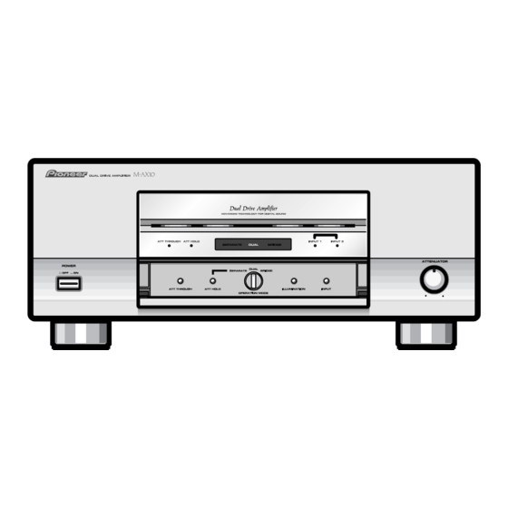
- Page 17 M-AX10 FRONT ASSY (AWX7276) SWITCHES S901 : ATT THROUGH S902 : ATT HOLD S903 : INPUT S904 : ILLUMINATION S905 : MODE...
- Page 18 M-AX10 3.4 INPUT (L), INPUT (R) ASSY INPUT(L) ASSY (AWX7273) 12dB FLAT AMP JA101 JA102...
- Page 19 M-AX10 J201 CN401 JA201 CN201 INPUT(R) ASSY (AWX7274) JA202 CN714 SIGNAL ROUTE : AUDIO SIGNAL DAC VR J101 CN301 CN101 CN713...
- Page 20 M-AX10 14dB POWER AMP 3.5 V.AMP (L) ,V.AMP (R) ASSY V. AMP(L) ASSY (AWX7278) DC ADJ(HL) J101 CN715 DC ADJ(LL)
- Page 21 M-AX10 SIGNAL ROUTE : AUDIO SIGNAL J401 J301 CN607 CN507 CN608 J402 CN508 J302 J201 CN401 CN602 CN402 CN502 CN403 CN716...
- Page 22 M-AX10 3.6 C.AMP (L), C.AMP (R) ASSY CN505 C. AMP(L) ASSY CURRENT AMP (KU/CA : AWX7673) NY : AWX7280) CN507 J301 CN508 J302 IDLE ADJ(HL) CN303 IDLE ADJ(LL)
- Page 23 M-AX10 To C2,C4 C. AMP(R) ASSY (KU/CA : AWX7674) NY : AWX7281) J401 J402 CN403 SIGNAL ROUTE : AUDIO SIGNAL To C1,C3...
-
Page 24: Pcb Connection Diagram
M-AX10 4. PCB CONNECTION DIAGRAM 4.1 JOINT, SW, LED, VR ASSY NOTE FOR PCB DIAGRAMS : 1. Part numbers in PCB diagrams match those in the schematic SIDE A diagrams. JOINT ASSY 2. A comparison between the main parts of PCB and schematic diagrams is shown below. - Page 25 M-AX10 SIDE B JOINT ASSY (ANP7281-A) LED ASSY SW ASSY VR ASSY (ANP7281-A) (ANP7281-A) (ANP7282-C)
- Page 26 M-AX10 4.2 POWER SUPPLY ASSY POWER SUPPLY ASSY SIDE A CN601 CN712 CN901 AC POWER CODE POWER TRANSFORMER POWER TRANSFORMER CN701 CN711 CN501 (ANP7282-C) Q812 Q808 Q804 IC801 IC802 IC805 Q810 Q806 Q802 IC804 IC803 Q811 Q807 Q803 Q809 Q805...
- Page 27 M-AX10 POWER SUPPLY ASSY SIDE B (ANP7282-C) Q821 Q816 Q818 Q820 Q814 Q817 Q819 Q815 Q813...
- Page 28 M-AX10 4.3 FRONT ASSY FRONT ASSY SIDE A CN761 CN804 CN751 (ANP7282-C) IC903 IC902 Q904 Q901 Q918 Q935 Q932 Q946 Q943 Q903 Q902 Q934 Q933 Q949 Q947 Q952 IC904 Q945 Q942 IC901...
- Page 29 M-AX10 FRONT ASSY SIDE B (ANP7282-C) Q916 Q919 Q928 Q930 Q907 Q950 Q915 Q926 Q951 Q948 Q917 Q914...
- Page 30 M-AX10 4.4 INPUT(L) ASSY INPUT(L) ASSY SIDE A CN301 CN713 Q101 Q107 Q111 IC101 IC102 Q119 Q120 Q129–Q131 Q106 Q110 Q114 (ANP7281-A) INPUT(L) ASSY SIDE B Q116 Q117 Q126–Q128 Q115 Q118...
- Page 31 M-AX10 4.5 INPUT(R) ASSY INPUT(R) ASSY SIDE A CN401 CN714 Q220 Q219 IC202 IC201 Q211 Q207 Q201 Q229–Q231 Q214 Q210 Q206 (ANP7281-A) INPUT(R) ASSY SIDE B Q226–Q228 Q217 Q216 Q218 Q215...
- Page 32 M-AX10 4.6 V. AMP(L) ASSY SIDE A V. AMP(L) ASSY CN715 CN508 CN502 CN507 J101 VR301 VR302 Q321 Q309 Q305 Q301 Q333 Q334 (ANP7294-C) Q324 Q316 Q308 Q304 SIDE B V. AMP(L) ASSY Q341 Q325 Q331 Q332 Q329 Q337 Q340...
- Page 33 M-AX10 4.7 V. AMP(R) ASSY SIDE A V. AMP(R) ASSY CN716 CN608 CN602 CN607 J201 VR402 VR401 Q433 Q401 Q405 Q409 Q421 Q434 (ANP7294-C) Q404 Q408 Q416 Q424 SIDE B V. AMP(R) ASSY Q440 Q437 Q429 Q432 Q431 Q425 Q441...
- Page 34 M-AX10 4.8 C. AMP(L) ASSY C. AMP(L) ASSY VR502, VR501 Q515 Q513 CN303 SIDE A J302 J301 (ANP7294-C) C. AMP(L) ASSY Q502, Q501 Q520, Q519 SIDE B Q504, Q506, Q508, Q510 Q518 Q512, Q511, Q517 Q507, Q509, Q505, Q503...
- Page 35 M-AX10 4.9 C. AMP(R) ASSY C. AMP(R) ASSY VR602, VR601 Q615 Q613 CN403 SIDE A J401 J402 (ANP7294-C) C. AMP(R) ASSY Q601, Q602 Q619, Q620 SIDE B Q608, Q610, Q606, Q604 Q618 Q617, Q611, Q612 Q603, Q605, Q607, Q609...
-
Page 36: Pcb Parts List
562 × 10 → 5621 ............RN1/4PC 5 6 2 1 CONTRAST OF PCB ASSEMBLIES Part No. Mark Symbol and Description Remarks M-AX10 /KU/CA M-AX10 /NY POWER AMP ASSY AWH7003 AWH7002 V. AMP (L) ASSY AWX7278 AWX7278 V. AMP (R) ASSY... - Page 37 M-AX10 Mark No. Description Part No. Mark No. Description Part No. R819-R822 RS1/10S301J JOINT ASSY R836-R838 RS1/10S3R3J R805-R808 RS1LMF103J COILS AND FILTERS Other Resistors RS1/10S L711,L712 RTF1167 OTHERS CAPACITORS CN805,CN806 10P MT CONNECTOR 1-173981-0 CN804 16P CONNECTOR 9604S-16C C711,C712 CEAT100M50...
- Page 38 M-AX10 Mark No. Description Part No. Mark No. Description Part No. C927,C954 CKSQYF103Z50 COILS AND FILTERS C901-C914,C923-C926 CKSQYF104Z50 L101 RTF1167 C931-C934,C951,C956 CKSQYF104Z50 SWITCHES AND RELAYS RESISTORS RY101-RY103 VSR1008 Other Resistors RS1/10S CAPACITORS C101,C102,C105-C108 (220pF) ACE7012 OTHERS C140 (47µF) ACH7116 C103,C104...
- Page 39 M-AX10 Mark No. Description Part No. Mark No. Description Part No. R503,R504 RS1/10S6801F C305-C308,C323-C326 CCSQCH270J50 R521,R522,R537,R538 RS1/10S8201F C311,C312 CEAT470M25 C315-C318 CEGA471M50 R509-R512,R531-R534 RS2LMFR22J C309,C310 CEHAZA470M10 R513,R514 RS3LMF2R2J VR501,VR502 (4.7KΩ) ACP7003 C331 CFTYA683J50 C337,C338 CSZSR100M16 Other Resistors RS1/10S RESISTORS OTHERS R303,R304...
- Page 40 M-AX10 Mark No. Description Part No. Mark No. Description Part No. R257,R258 RS1/10S1002F Other Resistors RS1/10S C. AMP (R) ASSY (AWX7674) OTHERS SEMICONDUCTORS J201 6P HOUSING SHIELD WIRE ADX7253 IC601,IC602 IC PROTECTOR(10A) AEK7022 JA201,JA202 PIN JACK(1P) AKB7102 Q603,Q604 2SA1162 CN201...
-
Page 41: Adjustment
M-AX10 6. ADJUSTMENT 6.2 DC OFFSET ADJUSTMENT 6.1 IDLE CURRENT ADJUSTMENT Adjust the DC offset with the power on immediately before fine The idle current is adjusted in two steps: coarse and fine. Note that adjustment of the idle current. -
Page 42: General Information
M-AX10 7. GENERAL INFORMATION 7.1 IC • The information shown in the list is basic information and may not correspond exactly to that shown in the schematic diagrams. • List of IC PD5508B9, DAC8043FP PD5508B9 (FRONT ASSY : IC901) • Control Microcomputer •... -
Page 43: Specifications
M-AX10 Following item "1."~"7." (P.43~P.51) describe about the specifications 1.2 BACKUP Mode of IC901 PD5508B9. Backup is performed when the AC power is turned off. SPRYH (port 16) and SPRYG (port 17) are set to "L" 10 ms after SPECIFICATIONS the BACKUP port becomes "L."... - Page 44 M-AX10 (2) POWER OFF 1.3 Last Memory Port 16 (SPRYH)(Pin16) is set to "L" 10 ms after POWER OFF Last memory writing to the EEPROM (IC904:AT24C01-10OC) is (port 26 (BACKUP)(Pin26) becomes "L"). performed each time a key is operated. Input-independent last memory is not provided.
- Page 45 M-AX10 Reset AC check 200 msec Register initial setting RAM initial setting when EEPROM read out is OK. RAM initial setting when EEPROM read out is NG. Timer [tminit] 50 msec INITCONT start INITCONT processing ACTION start Relay Timer [tmprot]...
- Page 46 M-AX10 3. Key Input (IC901) IC901 PD5508B9 36 (MD WKUP) IC901 37 (ATT.THROUGH) 38 (ATT.HOLD) Microcomputer 39 (INPUT) 40 (ILL) Key input, indicators and processes Contents of Process Key Input Indicator Port Process Port DUAL BRIDGE SEPARATE Alternates "H" and "L"...
- Page 47 M-AX10 Port 16 (SPRYH)(Pin16) is set to "L" 10 ms after ATT.THROUGH 3.1 Key Inputs switching signal input, and relay is set to OFF. A key input becomes valid after 40 ms, to eliminate chatter. After another 30 ms, the INDICATOR port is processed.
- Page 48 M-AX10 4.4 ILL Key Processing 4.2 INPUT switching INDICATOR port processing and switching process start 30 ms Each press of the key cycles Bright, Dark, Lamp Off, and LED after INPUT key input [port 39 (INPUT)(Pin39): "L"]. Off. No muting process is performed.
- Page 49 M-AX10 5. Mode Switching Processing (IC901) Select the mode of the speakers using the MODE switch (rotary switch). Any of three modes (BRIDGE, DUAL and SEPARATE) can be selected. IC901 PD5508B9 Table Mode select indicator processing Mode Indicator Contents of Process...
- Page 50 M-AX10 BRIDGE / DUAL PROCESSOR Binary Position Code Attenuation (dB) Serial Data Attenuation (dB) Serial Data 00000 00001 -2.0021 -0.5 -0.5021 00010 -4.0026 -1.0 -1.0016 00011 -6.0015 -1.5 -1.5013 00100 -8.0013 -2.0 -2.0021 00101 -10.0064 -2.5 -2.5023 00110 -12.0052 -3.0 -3.0001...
- Page 51 M-AX10 7.3 Warning when switching ATT.THROUGH from Switching (restoring the original setting) Switching OFF to ON Acknowledgment When ATT.THROUGH is switched from OFF to ON, the key of switching 20 msec 20 msec becomes valid when it is held pressed for 2 seconds.
-
Page 52: Protection Circuit
M-AX10 7.2 PROTECTION CIRCUIT The protection circuits are provided for this unit. When these protection circuits are activated ,the hardware muting is activated and muting and the output relays are controlled by the microcomputer. There are two protection circuits. 1) DC voltage detection at the output 2) Overcurrent detection due to the short circuit at the load end 1. - Page 53 M-AX10...
-
Page 54: Explanation
M-AX10 7.3 DESCRIPTIONS Wide-range linear circuit 7.3.1 Product Overview The wide range linear circuit has been enhanced to improve DC stability by newly employing highly accurate parts of 0.5% error Features of this product and single-chip dual transistors for a completely discrete structure Three-mode drive power amplifiers that uses no DC servo or operational amplifier. -
Page 55: Circuit Description
M-AX10 7.3.2 Circuit Description Block Diagram... - Page 56 M-AX10 Each mode of block diagram 12dB 14dB IN 2 Low ch 12dB 14dB IN 1 High ch DAC VR – Dual Drive Mode – 12dB 14dB IN 2 Full 12dB 14dB Range – IN 1 DAC VR – Bridge Drive Mode –...
- Page 57 INPUT switching clock is used. 40dBV (100Vrms) 4. 14-dB power amplifier block 40Vrms, 32dBV Pioneer's original "Direct-Energy MOSFET Amplifier" and "Wide- Bridge Range Linear Circuits" are mounted. The circuits function as the 30dBV 20Vrms, 26dBV inversion/noninversion switching amplifier on the high-channel side Maximum and as an inversion amplifier in BRIDGE mode.
-
Page 58: Panel Facilities And Specifications
Note that it will be maximaum volume. mode switch back to its original position. Pressing the button again will cancel the operation. The flashing will stop, and your M-AX10 will 5 ILLUMINATION return to normal. Pressing the ILLUMINATION button once, twice or... - Page 59 METHODS OF CONNECTION Bridge mode The M-AX10 has four built-in amplifier channels, which can be connected by means of three different operation modes: BRIDGE ,DUAL and SEPARATE. You may select the mode which best suits your purpose and the equipment you are co- nnecting to your M-AX10.
- Page 60 M-AX10 REAR SECTION INPUT 2 INPUT 1 This is an input terminal for connecting This is an input terminal for CD players,control amplifiers,channel connecting CD players,control dividers and other components. amplifiers,channel dividers and other components. SPEAKERS (L) SPEAKERS (R) These are terminal for These are terminal for right-hand left-hand speakers.
- Page 61 M-AX10 SPECIFICATIONS Amplifier Section Signal-to Noise ratio (IHF short circuit, A network (U.S model only) ATT THROUGH ON) When set to Bridge mode: INPUT 1,2 ................125dB Continuous average power output is 200 Watts* per channel, min.,at 6 ohms from 20 Herz to 20,000 Herz Channel separation(20Hz to 20 kHz) with no more than 0.2%** total harmonic distortion.
Need help?
Do you have a question about the M-AX10 and is the answer not in the manual?
Questions and answers