Table of Contents
Advertisement
SERVICE MANUAL
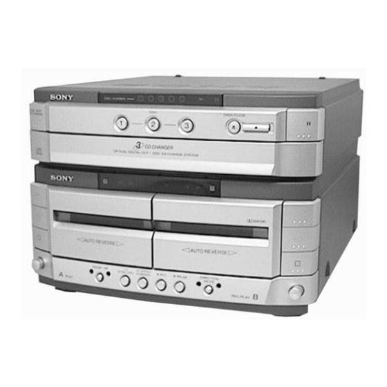
HTC-W555 is the deck and CD
section in MHC-W555/W777.
MICROFILM
HTC-W555
Model Name Using Similar Mechanism
CD Mechanism Type
CD
SECTION
Base Unit Type
Optical Pick-up Type
TAPE
Model Name Using Similar Mechanism
DECK
Tape Transport Mechanism Type
SECTION
SPECIFICATIONS
– 1 –
AEP Model
UK Model
E Model
Australian Model
Chinese Model
Tourist Model
HCD-H991AV
CDM38-5BD29A
BU-5BD29AL
KSS-213B/S-N
NEW
TCM-230AWR1
COMPACT DISC DECK
Advertisement
Table of Contents

Related Manuals for Sony HTC-W555


Summary of Contents for Sony HTC-W555
- Page 1 HTC-W555 SERVICE MANUAL AEP Model UK Model E Model Australian Model Chinese Model Tourist Model HTC-W555 is the deck and CD section in MHC-W555/W777. Model Name Using Similar Mechanism HCD-H991AV CD Mechanism Type CDM38-5BD29A SECTION Base Unit Type BU-5BD29AL Optical Pick-up Type...
- Page 2 WITH MARK ! ON THE SCHEMATIC DIAGRAMS AND IN THE PARTS LIST ARE CRITICAL TO SAFE OPERATION. REPLACE THESE COMPONENTS WITH SONY PARTS WHOSE PART NUMBERS APPEAR AS SHOWN IN THIS MANUAL OR IN SUPPLEMENTS PUBLISHED BY SONY. – 2 –...
-
Page 3: Table Of Contents
TABLE OF CONTENTS 1. SERVICING NOTE ............4 2. GENERAL ................7 3. DISASSEMBLY 3-1. Loading Panel ................ 8 3-2. Back Panel and CD Mechanism Deck ........8 3-3. Front Panel ................9 3-4. TC Mechanism Deck and Cassette Holder ......9 3-5. -
Page 4: Servicing Note
SECTION 1 SERVICING NOTE HOW TO OPEN THE DISC TRAY WHEN POWER SWITCH TURNS OFF 1 Remove the Case. 3 Pull-out the disc tray. Turn the cam to the direction of arrow. Note for Installation (ROTARY ENCODER) Note:When attaching the Base unit, Insert the BU cam section A into the groove of BU cam. - Page 5 Connection and Operations of the Unit by Itself This unit cannot be operated by itself as it does not come with a power supply. Connect STR-W555/W777 as shown in “Connection 1” before beginning servicing. Connection 1: If there is STR-W555/W777. STR-W555/W777 SYSTEM CABLE 17P AC IN...
- Page 6 Cold Reset NOTE: This is the mode for operating the unit by itself. Take note that the operating method differs when connected to the STR-W555/ W777. This method is described in the manuals of the STR-W555 and STR-W777. Refer to these manuals for details. This mode is used for initializing the RAM contents.
-
Page 7: General
SECTION 2 GENERAL Front Panel 2 3 4 11 12 13 LOCATION OF PARTS AND CONTROLS 17 π (Deck B stop) button 1 DISC SKIP/EX-CHANGE button 18 § (Deck B eject) button 2 DISC 1 button 3 DISC 2 button 19 Casette lid (Deck B) 4 DISC 3 button 20 DIRECTION MODE button... -
Page 8: Disassembly
SECTION 3 DISASSEMBLY Note: Follow the disassembly procedure in the numerical order given. 3-1. LOADING PANEL 3 Loading panel (Remove two claws) Two claws 2 Pull-out the disc tray. 1 Turn the cam to the direction of arrow. 3-2. BACK PANEL AND CD MECHANISM DECK !¢... -
Page 9: Front Panel
3-3. FRONT PANEL 2 Flat type wire 1 Flat type wire (17core, CNS104) (13core, CNS102) 3 Flat type wire (15core, CNS101) 4 Connector (CN113) 6 Lead (with connector) 8 Front panel (Remove the catcer) Catcher 7 Connector (CNP105) 5 Two screws (BVTP3x10) 3-4. -
Page 10: Disc Tray
3-5. DISC TRAY Note: When installing the Disc tray, pull around the flat type wire to pass through the claw A and claw B, as shown in the figure. 3 Flat type wire (8 core) 4 Two claws 2 Pull-out the disc tray. 5 Remove the disc tray. -
Page 11: Mechanical Adjustments
SECTION 4 SECTION 5 MECHANICAL ADJUSTMENTS ELECTRICAL ADJUSTMENTS Precaution Read before adjustments 1. Clean the following parts with a denatured alcohol-moistened To adjust the unit, operate the unit by itself using the conduction jig swab: (PFJ-1). record/playback heads pinch rollers erase head rubber belts For details on switching functions and fast forwarding the unit, etc. - Page 12 2. Turn the adjustment screw and check output peaks. If the peaks Tape Speed Adjustment (Deck B) do not match for L-CH and R-CH, turn the adjustment screw so that outputs match within 1 dB of peak. Note: Set the test mode using the following method and begin tape speed adjustment.
- Page 13 Record Bias Adjustment (Deck B) Record Level Adjustment (Deck B) Procedure: Procedure: 1. Press the p (CD) button while pressing the DIRECTION 1. Press the p (CD) button while pressing the DIRECTION MODE button. MODE button. 2. While pressing the p (CD) button, press the ª (TAPE A) 2.
- Page 14 CD SECTION E-F Balance (1 Track Jump) check oscilloscope Note: BD board 1. CD Block is basically constructed to operate without adjustment. Therefore, check each item in order given. TP (TEO) 2. Use YEDS-18 disc (3-702-101-01) unless otherwise indicated. TP (VC) 3.
-
Page 15: Diagrams
SECTION 6 DIAGRAMS 6-1. CIRCUIT BOARDS LOCATION REGULATOR board CD (P) board TC LED board TC (A) board MAIN board TC (P) board TC (B) board MOTOR (TURN) board CONNECTOR board BD board SENSOR board LEAF SW board MOTOR (SLIDE) board AUDIO board –... -
Page 16: Block Diagrams
HTC-W555 6-2. BLOCK DIAGRAMS – CD SECTION – IC107 CD DIGITAL D.OUT X101 16.9344MHz OPTICAL OPTICAL PICK-UP BLOCK FOCUS/TRACKING SERVO. RF AMP 89 • 90 IC101 (1/2) DETECTOR RF O LOUT1 L-CH DIGITAL SIGNAL PROCESSOR LOUT2 LOCK 29 LOCK R-CH IC103 C.OUT... -
Page 17: Deck Section
HTC-W555 – DECK SECTION – PB A/B S1008 S1004 MS OUT A CrO B CrO RV311 28 27 PLAYBACK IC611 A 120/70 LEVEL PB-A/B B 120/70 DECK A A IN PB OUT B IN PB L HP101 PB HEAD LM ON/... -
Page 18: Main Section
HTC-W555 M12V – MAIN SECTION – +12V REG +7.5V REG A+7.5V IC851 Q852 D+5V +5V REG +5V SW IC852 Q102-104 A+5V +7V REG M+7V RECT IC853 D901-904 -7.5V REG A-7.5V (CD R) Q855 R CH CNB108 (PB R) SYSTEM R CH... - Page 19 WAVEFORMS THIS NOTE IS COMMON FOR PRINTED WIR- ING BOARDS AND SCHEMATIC DIAGRAMS. (In addition to this, the necessary note is printed 1.3Vp-p in each block.) For schematic diagrams. 500mV/DIV, 500nsec/DIV Note: IC101 #£ RFO • All capacitors are in µF unless otherwise noted. pF: µµF 50 WV or less are not indicated except for electrolytics and tantalums.
-
Page 20: Printed Wiring Board - Cd Section
HTC-W555 6-3. PRINTED WIRING BOARD – CD SECTION – • See page 15 for Circuit Boards Location. • Semiconductor Location Ref. No. Location IC101 IC102 IC103 Q101 (Page 34) – 25 – – 26 –... -
Page 21: Schematic Diagram - Cd Section
HTC-W555 6-4. SCHEMATIC DIAGRAM – CD SECTION – • See page 23 for Waveforms. • See page 49 for IC Block Diagrams. • See page 52 for IC Pin Functions. (Page – 27 – – 28 –... -
Page 22: Schematic Diagram - Deck Section
HTC-W555 6-5. SCHEMATIC DIAGRAM – DECK SECTION – • See page 51 for IC Block Diagrams. (Page 36) – 29 – – 30 –... -
Page 23: Printed Wiring Board - Deck Section
HTC-W555 6-6. PRINTED WIRING BOARD – DECK SECTION – • See page 15 for Circuit Boards Location. (Page 33) – 31 – – 32 –... -
Page 24: Printed Wiring Board - Main Section
HTC-W555 6-7. PRINTED WIRING BOARD – MAIN SECTION – (Page 41) • See page 15 for Circuit Boards Location. (Page 39) (Page 26) (Page 41) (Page 47) (Page 47) (Page • Semiconductor (Page 31) Location Ref. No. Location D110 D855... -
Page 25: Schematic Diagram - Main (1/2) Section
HTC-W555 6-8. SCHEMATIC DIAGRAM – MAIN (1/2) SECTION – (Page 39) (Page 46) (Page 46) (Page 28) (Page 30) (Page 37) (Page 38) (Page 38) (Page 38) – 35 – – 36 –... -
Page 26: Schematic Diagram - Main (2/2) Section
HTC-W555 6-9. SCHEMATIC DIAGRAM – MAIN (2/2) SECTION – • See page 33 for Printed Wiring Board. • See page 57 for IC Pin Functions. (Page 36) (Page 35) (Page 36) (Page 36) (Page 43) (Page 43) (Page 43) – 37 –... -
Page 27: Printed Wiring Board - Leaf Sw Section
6-10. PRINTED WIRING BOARD – LEAF SW SECTION – • See page 15 for Circuit Boards Location. (Page 33) 6-11. SCHEMATIC DIAGRAM – LEAF SW SECTION – (Page 36) – 39 –... -
Page 28: Printed Wiring Board - Panel Section
HTC-W555 6-12. PRINTED WIRING BOARD – PANEL SECTION – • See page 15 for Circuit Boards Location. (Page 33) (Page 33) (Page 33) – 41 – – 42 –... -
Page 29: Schematic Diagram - Panel Section
HTC-W555 6-13. SCHEMATIC DIAGRAM – PANEL SECTION – (Page 43) (Page 43) (Page 43) – 43 – – 44 –... -
Page 30: Schematic Diagram - Cd Motor Section
HTC-W555 6-14. SCHEMATIC DIAGRAM – CD MOTOR SECTION – • See page 51 for IC Block Diagrams. (Page 35) (Page 35) – 45 – – 46 –... -
Page 31: Printed Wiring Board - Cd Motor Section
HTC-W555 6-15. PRINTED WIRING BOARD – CD MOTOR SECTION – • See page 15 for Circuit Boards Location. (Page 34) (Page 34) – 47 – – 48 –... -
Page 32: Ic Block Diagrams
6-16. IC BLOCK DIAGRAMS • CD section IC101 CXA1992AR – RF SUMMING PD2 IV PD1 IV FE_BIAS SENS2 ↓ – SENS1 LASER POWER CONTROL F IV AMP FE AMP – C. OUT E IV AMP – DFCT XRST – LEVEL S DATA FO. - Page 33 IC102 BA5941FP – + – + – LEVEL SHIFT LEVEL SHIFT LEVEL SHIFT – LEVEL SHIFT – – + – – + – MUTE IC103 CXD2519Q 80 79 78 77 76 75 74 73 72 71 70 69 68 67 66 65 64 63 62 61 60 59 58 57 56 55 54 53 52 51 LRCK AVSS WDCK...
- Page 34 • Deck section IC602 uPC1330HA INVERTER COMPARATER SW P1 CONT GND SW R1 GND SW P2 GND SW R2 • CD motor section IC701 M54641L REFERENCE POWER OUT2 INPUT AMP. AMP. CONTROL POWER OUT1 INPUT AMP. AMP. IC801 BA6286N PO WER SAVE VREF OUT2...
-
Page 35: Ic Pin Functions
6-17. IC PIN FUNCTIONS • IC101 FOCUS/TRACKING/SLED SERVO RF AMP (CXA1992AR) Function Pin No. Pin Name Focus error amplifier output Connected internally to the window comparator input for bias adjustment Focus error input Capacitor connection pin for defect time constant FDFCT Ground this pin through a capacitor for cutting the focus servo high-frequency gain External time constant setting pin for boosting the focus servo low-frequency... - Page 36 Pin Name Function Pin No. RF summing amplifier inverted input The RF amplifier gain is determined by the resistance connected between this pin and RF M RFO pin RFTC External time constant setting pin during RF level control APC amplifier output APC amplifier input RF I-V amplifier inverted input Connect these pins to the photo diode A+C and B+D pins...
- Page 37 • IC103 DIGITAL SIGNAL PROCESSOR (CXD2519Q) Pin Name Function Pin No. – +5V power supply – Ground Lch “L” detection flog (Not used) LMUT Rch “L” detection flog (Not used) RMUT Test output (Not used) ACDT Master clock divider output (Not used) CKOUT Clock input for SQSO read out SQCK...
- Page 38 Pin Name Function Pin No. Analog ground AVSS – CLTV Control voltage input for VCO Analog power supply AVDD – EFM signal input Asymmetry circuit constant current input BIAS Asymmetry comparate voltage input ASYI ASYO EFM full swing output (“L” =V , “H”...
- Page 39 Pin Name Function Pin No. — – Not used AVSS Analog ground – AVDD Analog power supply – AOUT1 Lch analog output AIN1 Lch opamp input LOUT1 Lch line output AVSS Analog ground – XVDD Master clock power supply – XTAI X’tal oscillator circuit input XTAO...
- Page 40 • IC101 MASTER CONTROL (uPD780016AYGF-013-3BA) Pin No. Pin Name Function CAPM-EMG (+) Capstan motor control 1 (+) signal output 2 to 7 LED1 to LED6 Not used – Ground X’tal (5MHz) – Power supply (+5V) Not used – Power supply (+5V) RESET Reset signal input Ground...
- Page 41 Pin Name Function Pin No. TBL-L Table motor control output TBL-R Not used LOAD-OUT Loading motor control signal output LOAD-IN CD-PAUSE LED IN/OFF control output DECO2 LED IN/OFF control output CD-PLAY LED IN/OFF control output EXIST3 LED IN/OFF control output EXIST1 LED IN/OFF control output DISC3...
-
Page 42: Exploded Views
SECTION 7 EXPLODED VIEWS NOTE: The components identified by • Items marked “*” are not stocked since they are mark ! or dotted line with mark seldom required for routine service. Some delay ! are critical for safety. should be anticipated when ordering these items. Replace only with part number •... -
Page 43: Front Panel Section
X-4950-011-1 FRONT PANEL ASSY 4-210-045-01 DAMPER X-4950-013-1 ESCUTCHEON (TC) ASSY 4-977-358-11 CUSHION X-4950-012-1 ESCUTCHEON (CD) ASSY 3-019-456-01 SCREW STEP 4-962-708-11 EMBLEM (4-A), SONY 4-900-888-01 EJECT (LEVER-L) 4-900-881-01 BUTTON (EJECT A) 4-900-889-01 EJECT (LEVER-R) 4-900-882-01 BUTTON (EJECT B) * 71 1-669-420-11 CD (P) BOARD 4-951-620-01 SCREW (2.6X8), +BVTP... -
Page 44: Cd Mechanism Section 1 (Cdm38-5Bd29A)
7-3. CD MECHANISM SECTION 1 (CDM38-5BD29A) M701 Ref. No. Part No. Description Remark Ref. No. Part No. Description Remark 4-981-789-21 BRACKET (2), YOKE 4-977-941-01 BEARING (WORM) 4-977-945-01 TRAY (TURN) * 209 1-658-576-11 SENSOR BOARD X-4946-665-1 SHAFT ASSY, WORM 4-934-376-01 SHAFT (ROLLER) 4-977-943-01 BELT (TURN) (1.2) 4-977-956-01 WHEEL, WORM 4-981-187-01 COLLAR (WORM) -
Page 45: Cd Mechanism Section 2 (Cdm38-5Bd29A)
7-4. CD MECHANISM SECTION 2 (CDM38-5BD29A) supplied not supplied M801 BU-5BD29A S811 Ref. No. Part No. Description Remark Ref. No. Part No. Description Remark 4-981-789-11 BRACKET (2), YOKE * 260 X-4946-668-1 CHASSIS (CDM) ASSY 4-977-954-01 PULLEY (SL) 4-977-953-01 GEAR (SL-A) 4-985-672-01 SCREW (+PTPWH M2.6X6), FLOATING 4-977-955-01 GEAR (SL-B) * 262... -
Page 46: Base Unit Section (Bu-5Bd29A)
7-5. BASE UNIT SECTION (BU-5BD29A) M101 M102 The components identified by mark ! or dotted line with mark ! are critical for safety. Replace only with part number specified. Ref. No. Part No. Description Remark Ref. No. Part No. Description Remark ! 301 8-848-379-31 OPTICAL PICK-UP BLOCK KSS-213BA/F-NP... -
Page 47: Tc Mechanism Section 1 (Tcm230Awr1)
7-6. TC MECHANISM SECTION 1 (TCM230AWR1) * NOTE: Two types of parts which are not interchangeable are available for the Head deck (A) ASSY and Head deck (B) ASSY. When replacing the parts, refer to the following figure, and use the appropriate part Parts with “P”... -
Page 48: Tc Mechanism Section 2 (Tcm230Awr1)
7-7. TC MECHANISM SECTION 2 (TCM230AWR1) * NOTE: Two types of parts which are not interchangeable are available for the mechanical block assembly. When replacing the parts, refer to the following figure, and use the appropriate part. Parts with “P” mark: 230PWR1 Parts without “P”... -
Page 49: Electrical Parts List
SECTION 8 AUDIO ELECTRICAL PARTS LIST Note: • Due to standardization, replacements in the parts list • CAPACITORS The components identified by uF : µ F may be different from the parts specified in the mark ! or dotted line with mark •... - Page 50 AUDIO Ref. No. Part No. Description Remark Ref. No. Part No. Description Remark R601 1-249-409-11 CARBON 1/4W F C130 1-164-336-11 CERAMIC CHIP 0.33uF R602 1-249-409-11 CARBON 1/4W F C131 1-164-346-11 CERAMIC CHIP R608 1-249-409-11 CARBON 1/4W F R609 1-249-433-11 CARBON 1/4W C140 1-110-501-11 CERAMIC CHIP...
- Page 51 CD (P) Ref. No. Part No. Description Remark Ref. No. Part No. Description Remark R104 1-216-093-00 METAL CHIP 1/10W R190 1-216-097-91 RES, CHIP 100K 1/10W R105 1-216-088-00 METAL CHIP 1/10W R191 1-216-105-91 RES, CHIP 220K 1/10W R106 1-216-088-00 METAL CHIP 1/10W R107 1-216-088-00 METAL CHIP...
- Page 52 CD (P) CONNECTOR LEAF SW MAIN Ref. No. Part No. Description Remark Ref. No. Part No. Description Remark < SWITCH > R1002 1-249-409-11 CARBON 1/4W F R1003 1-249-414-11 CARBON 1/4W F S270 1-762-751-11 SWITCH, TACTILE (fl) R1004 1-247-834-11 CARBON 1.3K 1/4W S271 1-762-751-11 SWITCH, TACTILE (p)
- Page 53 100uF C863 1-126-929-11 ELECT 4700uF Q343 8-729-029-66 TRANSISTOR DTC114ESA Q852 8-729-018-60 TRANSISTOR 2SD2012-LC C867 1-126-967-11 ELECT 47uF Q855 8-729-018-59 TRANSISTOR 2SB1375(LB SONY) C868 1-126-934-11 ELECT 220uF C869 1-126-967-11 ELECT 47uF < RESISTOR > C870 1-164-159-11 CERAMIC 0.1uF C871 1-164-159-11 CERAMIC 0.1uF...
- Page 54 MAIN MOTOR (SLIDE) Ref. No. Part No. Description Remark Ref. No. Part No. Description Remark R152 1-249-429-11 CARBON 1/4W R359 1-249-435-11 CARBON 1/4W R153 1-249-419-11 CARBON 1.5K 1/4W F R704 1-249-417-11 CARBON 1/4W F R154 1-249-419-11 CARBON 1.5K 1/4W F R155 1-249-426-11 CARBON 5.6K...
- Page 55 MOTOR (TURN) SENSOR TC(A) TC(B) TC(P) TC LED REGULATOR Ref. No. Part No. Description Remark Ref. No. Part No. Description Remark 1-658-577-11 MOTOR (TURN) BOARD 1-669-422-11 TC (A) BOARD ******************* ************ < CAPACITOR > < RESISTOR > C701 1-162-306-11 CERAMIC 0.01uF R209 1-249-415-11 CARBON...
- Page 56 TC LED Ref. No. Part No. Description Remark D206 8-719-071-42 DIODE SEL5723C-TP15 (9 (DECK A)) < TRANSISTOR > Q201 8-729-029-21 TRANSISTOR DTA114ESA-TP Q202 8-729-029-21 TRANSISTOR DTA114ESA-TP Q203 8-729-029-21 TRANSISTOR DTA114ESA-TP Q204 8-729-029-21 TRANSISTOR DTA114ESA-TP Q205 8-729-029-21 TRANSISTOR DTA114ESA-TP Q206 8-729-029-21 TRANSISTOR DTA114ESA-TP <...
- Page 57 HTC-W555 Sony Corporation 98F0972-1 Printed in Japan © 1998. 6 9-922-906-11 Home A&V Products Company Published by Quality Assurance Dept. – 74 – (Shibaura)
Need help?
Do you have a question about the HTC-W555 and is the answer not in the manual?
Questions and answers