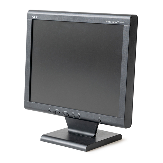
NEC MultiSync LCD1550V Service Manual
Color monitor
Hide thumbs
Also See for MultiSync LCD1550V:
- Service manual (101 pages) ,
- User manual (48 pages) ,
- Dimensional drawing (1 page)
Table of Contents
Advertisement
SERVICE MANUAL
COLOR MONITOR
MODELS LCD1550V-1 (B)/-BK(B)
This model changed a LCD panel (manufactured by Hannstar) from the original model.
Use the applicable service manual which surely confirms the model number of the
NAME PLATE, INSTRUCTION.
Refer to the page which the point of view of the model number is mentioned in.
• Model number : LA-15R02 / LA-15R02-BK
• Model number : LA-15R02-1 / LA-15R02-1-BK
NEC-MITSUBISHI ELECTRIC VISUAL SYSTEMS CORPORATION
MultiSync
Maintenance is performed by the original service manual (Part No.
599910571).
Maintenance is performed using this service manual.
JUNE 2002
PART NO. 599910588
LCD1550V
200206
08109741
08109742
Advertisement
Chapters
Table of Contents

Related Manuals for NEC MultiSync LCD1550V


Summary of Contents for NEC MultiSync LCD1550V
-
Page 1: Service Manual
• Model number : LA-15R02 / LA-15R02-BK Maintenance is performed by the original service manual (Part No. 599910571). • Model number : LA-15R02-1 / LA-15R02-1-BK Maintenance is performed using this service manual. NEC-MITSUBISHI ELECTRIC VISUAL SYSTEMS CORPORATION JUNE 2002 200206 08109741 08109742... - Page 2 WARNING The SERVICE PERSONNEL should have the appropriate technical training, knowledge and experience necessary to: • Be familiar with specialized test equipment, and • Be careful to follow all safety procedures to minimize danger to themselves and their coworkers. To avoid electrical shocks, this equipment should be used with an appropriate power cord. This equipment utilized a micro-gap power switch.
- Page 3 Point of view of the model number NAME PLATE, INSTRUCTION (White model) Model number Original model: LA-15R02 Hannstar LCD model: LA-15R02-1 NAME PLATE, INSTRUCTION (Black model) Model number Original model: LA-15R02-BK Hannstar LCD model: LA-15R02-1-BK...
- Page 4 CONTENTS Page No. USER'S MANUAL ------------------------------------------------------------------- 1-1 SERIAL NUMBER INFORMATION --------------------------------------------- 2-1 DISASSEMBLY ----------------------------------------------------------------------- 3-1 ADJUSTMENT PROCEDURES -------------------------------------------------- 4-1 INSPECTION --------------------------------------------------------------------------- 5-1 TROUBLE SHOOTING ------------------------------------------------------------- 6-1 CIRCUIT DESCRIPTION ----------------------------------------------------------- 7-1 REPLACEMENT PARTS LIST --------------------------------------------------- 8-1 BLOCK DIAGRAM ------------------------------------------------------------------- 9-1 SCHEMATIC DIAGRAMS -------------------------------------------------------- 10-1...
- Page 5 USER'S MANUAL MultiSync LCD1550V User’s Manual UÏivatelská pfiíruãka Bedienerhandbuch δηγίες ρήσης Manual del usuario Manuel Utilisateur Manuale utente Gebruikershandleiding Podr´cznik u˝ytkownika Руководство пользователя Kullan∂c∂ Klavuzu...
- Page 6 Council Directive 73/23/EEC: – EN 60950 Council Directive 89/336/EEC: – EN 55022 – EN 61000-3-2 – EN 61000-3-3 – EN 55024 and marked with NEC-Mitsubishi Electric Visual Systems, Corp. MS Shibaura Bldg., 13-23, Shibaura 4-chome, Minato-Ku, Tokyo 108-0023, Japan...
- Page 7 TCO’99 This is a translation of the original English TCO'99 document. MultiSync LCD1550V White Model (LA-15R02 and LA-15R02-1) Congratulations! You have just purchased a TCO’99 approved and labeled product! Your choice has provided you with a product developed for professional use. Your purchase has also contributed...
- Page 8 The requirements cover a wide range of issues: environment, ergonomics, usability, emission of electrical and magnetic fields, energy consumption and electrical and fire safety. The environmental demands concern restrictions on the presence and use of heavy metals, brominated and chlorinated flame retardants, CFCs (freons) and chlorinated solvents, among other things.
- Page 9 Cadmium** Cadmium is present in rechargeable batteries and in the colourgenerating layers of certain computer displays. Cadmium damages the nervous system and is toxic in high doses. TCO’99 requirement states that batteries, the colourgenerating layers of display screens and the electrical or electronics components must not contain any cadmium.
- Page 10 TCO’95 This is a translation of the original English TCO'95 document. MultiSync LCD1550V Black Model (LA-15R02-BK and LA-15R02-1-BK) Congratulations! You have just purchased a TCO’95 approved and labeled product! Your choice has provided you with a product developed for professional use. Your purchase has also...
- Page 11 The environmental demands concern restrictions on the presence and use of heavy metals, brominated and chlorinated flame retardants, CFCs (freons) and chlorinated solvents, among other things. The product must be prepared for recycling and the manufacturer is obliged to have an environmental plan which must be adhered to in each country where the company implements its operational policy.
- Page 12 Cadmium** Cadmium is present in rechargeable batteries and in the colourgenerating layers of certain computer displays. Cadmium damages the nervous system and is toxic in high doses. TCO’95 requirement states that batteries may not contain more than 25 ppm (parts per million) of cadmium. The colourgenerating layers of display screens must not contain any cadmium.
- Page 13 English Deutsch Ελληνικά Español Français Italiano Nederlands Русский...
- Page 14 Caution: When operating the MultiSync LCD1550V with a 220-240V AC power source in Europe, use the power cord provided with the monitor. In the UK, a BS approved power cord with a moulded plug has a Black (five Amps) fuse installed for use with this equipment.
- Page 15 Contents Your new NEC MultiSync LCD monitor box* should contain the following: • MultiSync LCD1550V monitor with tilt base • Power Cord(s) • Video Signal Cable • User’s Manual • CD ROM (includes complete User’s Manual in PDF format). To see the User’s Manual, Acrobat Reader 4.0 must be installed on your PC.
-
Page 16: Quick Start
For Mac: Connect the MultiSync LCD1550V Macintosh cable adapter to the computer (Figure B.1). Attach the 15-pin mini D-SUB end of the appropriate signal cable to the MultiSync LCD1550V Macintosh cable adapter (Figure B.1). Tighten all screws. 4. Connect the 15-pin mini D-SUB of the video signal cable to the appropriate connector on the back of the monitor (Figure C.1). -
Page 17: English
Refer to the Controls section of this User’s Manual for a full description of these OSM controls. NOTE: If you have any problems, please refer to the Troubleshooting section of this User’s Manual. Figure A.1 Macintosh Cable Adapter (not included) Macintosh G3 and G4 do not need a... -
Page 18: Remove Monitor Stand For Mounting
Connector cover Cable cover Clip B Figure C.1 Vacation Switch Power Button Figure D.1 Tilt Grasp both sides of the monitor screen with your hands and adjust the tilt as desired (Figure TS.1). Remove Monitor Stand for Mounting To prepare the monitor for alternate mounting purposes: 1. - Page 19 4. Remove the 4 screws connecting the monitor to the stand and lift off the stand assembly (Figure R.2) the monitor is now ready for mounting in an alternate manner. 5. Connect the AC cord and signal cable to the back of the monitor (Figure R.3).
-
Page 20: English
Figure R.2 Non-abrasive surface Figure R.3 7. This LCD monitor is designed for use with a flexible arm. Please use the attached screws (4pcs) when mounting. To meet the safety requirements the monitor must be mounted to an arm which guaranties the necessary stability under consideration of the weight of the monitor. -
Page 21: English
Replace screws Thickness of bracket (arm) 2.0 ~ 3.2 mm Tighten all screws 75 mm 75 mm 4 SCREWS (M4) (MAX depth: 8.5 mm If use other screw, check depth of hole. Weight of LCD assembly: 3.2kg (MAX) English-8 1-17... -
Page 22: Osm (On-Screen-Manager) Controls
Controls OSM (On-Screen-Manager) Controls The OSM controls on the front of the monitor function as follows: To access OSM press any of the control buttons ( , , -, +, NEXT). Control Menu EXIT Exits the OSM controls. Exits to the OSM main menu. CONTROL / Moves the highlighted area left/right to select control menus. -
Page 23: Auto Adjust
Auto Adjust Automatically adjusts the Image Position, the H. Size and Fine setting. Position Controls LEFT/RIGHT Controls Horizontal Image Position within the display area of the LCD. DOWN/UP Controls Vertical Image Position within the display area of the LCD. H. SIZE Adjusts the horizontal size by increasing or decreasing this setting. - Page 24 OSM TURN OFF The OSM control menu will stay on as long as it is use. In the OSM Turn Off submenu, you can select how long the monitor waits after the last touch of a button to shut off the OSM control menu. The preset choices are 10, 20, 30, 45, 60 and 120 seconds.
- Page 25 OSM Warning OSM Warning menus disappear with Exit button. NO SIGNAL: This function gives a warning when there is no signal present. After power is turned on or when there is a change of input signal or video is inactive, the No Signal window will appear.
-
Page 26: Recommended Use
Recommended Use Safety Precautions and Maintenance FOR OPTIMUM PERFORMANCE, PLEASE NOTE THE FOLLOWING WHEN SETTING UP AND USING THE MULTISYNC LCD COLOUR MONITOR: • DO NOT OPEN THE MONITOR. There are no user serviceable parts inside and opening or removing covers may expose you to dangerous shock hazards or other risks. - Page 27 • Allow adequate ventilation around the monitor so that heat can properly dissipate. Do not block ventilated openings or place the monitor near a radiator or other heat sources. Do not put anything on top of monitor. CAUTION • The power cable connector is the primary means of detaching the system from the power supply.
- Page 28 • Avoid displaying fixed patterns on the monitor for long periods of time to avoid image persistence (after-image effects). • Get regular eye checkups. Ergonomics To realize the maximum ergonomics benefits, we recommend the following: • Use the preset Size and Position controls with standard signals. •...
- Page 29 Printed in Taiwan HD67NM55101 1-25...
-
Page 30: Serial Number Information
Serial Number Information Refer to the serial number information shown below. EX.) SERIAL NUMBER LABEL (White model) Model Name : LCD1550V-1 : LCD1550V-1-BK (Black model) SERIAL NO. : g g g g g g g g g Manufactured Year : ( Last digit ) Manufactured Month : January to September... - Page 31 DISASSEMBLY g Before you disassemble the set, turn off power and pull out the power plug. g Use the proper screwdriver. If oversize or undersize screwdriver is used, screws may be damaged. g Assembly is the opposite process of disassembly. SYMBOL CODE(Compal) CODE(NMV)
- Page 32 SYMBOL CODE(Compal) CODE(NMV) DESCRIPTION CABINET COLOR FANM5516100 79PP0587 CABINET BACK ASSY White FANM5516200 79PP0606 CABINET COVER ASSY(BK-A) Black #2CPITS*3*12*3AF White #2CPITS*3*12*3KF Black...
- Page 33 SYMBOL CODE(Compal) CODE(NMV) DESCRIPTION CPIMS(CUP)*3*6*3AF SCREW SPECIAL SHIELD PCB ASSY SYMBOL CODE(Compal) CODE(NMV) DESCRIPTION #2CPITS*3*12*3AF 454A5267001 79PP0584 PCBA KEY/B VK-530 LNM555G...
- Page 34 SYMBOL CODE(Compal) CODE(NMV) DESCRIPTION CABINET COLOR CPIMS(CUP)*3*6*3AF 461A7367004 79PP0860 FIRMWARE CTRL/B VL-543 LN White 461A7367005 79PP0868 FIRMWARE CTRL/B VL-543 LN Black SYMBOL CODE(Compal) CODE DESCRIPTION CABINET COLOR CPIMS(CUP)*3*6*3AF SPECIAL WASHER 4*8*15BF CFIMS*3*6*3KF 453A7367001 79PP0801 PCBA POWER/B VP-543 LNS55 453A7567001 79PP0802 PCBA INVERTER/B VI-543 LN DC020149900 79PP0806...
- Page 35 SYMBOL CODE(Compal) CODE(NMV) DESCRIPTION CABINET COLOR #2CPITS*3*12*3AF FANM5515100 79PP0586 CABINET FRONT ASSY White FANM5515200 79PP0605 CABINET FRONT ASSY(BK-A) Black SYMBOL CODE(Compal) CODE(NMV) DESCRIPTION CPIMS*2.5**4*3AF...
- Page 36 CABINET COLOR HINGE L HINGE R FANM5523100 79PP0620 STAND FRONT NM5523 ABS+PC White FANM5523200 79PP0695 STAND FRONT NM5523 ABS+PC Black BRACKET HINGE FANM5517100 79PP0618 BASE ASSY NM5517 ABS+PC M White FANM5517200 79PP0693 BASE ASSY-NEC NM5517 ABS+ Black SL-CPIMS*4*8*15BF ---- SL-CPIMS*4*16*15BF...
-
Page 37: Table Of Contents
ADJUSTMENT PROCEDURES TABLE OF CONTENTS Page 1. Application --------------------------------------------------------------------------------------------- 2-2 2. Adjustment conditions ------------------------------------------------------------------------------ 2-2 2.1 Time for adjustment ------------------------------------------------------------------------------- 2-2 2.2 Measuring instruments, jigs, and tools ------------------------------------------------------- 2-2 2.3 Power-supply voltage ----------------------------------------------------------------------------- 2-2 2.4 Aging -------------------------------------------------------------------------------------------------- 2-2 3. Set adjustments -------------------------------------------------------------------------------------- 2-3 3.1 Power ON -------------------------------------------------------------------------------------------- 2-3... -
Page 38: Application
1. Application This adjustment specification shall be applied to the adjustment of the LCD1550V (LA-15R02-1) / LCD1550V-BK (LA-15R02-1-BK). 2. Adjustment conditions 2.1 Time for adjustment Adjustment of a unit to be adjusted shall be carried out only at the time of the adjustment of the set as a whole. 2.2 Measuring instruments, jigs, and tools The measuring instruments, jigs, and tools required at the time of the adjustment of the unit to be adjusted shall be as specified below. -
Page 39: Set Adjustments
3. Set adjustments 3.1 Power ON 1) Insert the AC power cable in a wall outlet, or press the POWER key thereafter. Confirm that the LED is lit in amber (or that an OSM of [NO SIGNAL] is displayed). * The product shall be regarded as an NG item unless the LED is lit in amber even when the AC power cable is inserted in a wall outlet or the POWER key is pressed. -
Page 40: Factory Mode
3.2 Factory mode Mention the contents of the service menu letter Warning message Color of frame Service: Cyan How to enter Service mode 1. Open Information menu (Signal information) 2. Press “3”+”4”+”RESET” 3. Indicate warning message 4. Press Next then enter Service mode Or Press EXIT to close OSM menu OSM Flame is CYAN How to use Service mode... - Page 41 Page2: The page can adjust RGB offset and gain. 1. Press 3 or 4 to move cursor on AUTO GAIN or AUTO OFFSET. 2. Press “+” or “-“ can auto balance. How to exit Service mode Press exit key and then close OSM menu (Service mode) When turn off monitor in Service mode, it should exit from Service mode.
- Page 42 Page 3 : F/W ver Indicate F/W version : Auto ADJUST COUNT Indicate total time that Auto Adjustment (Contrast, Auto adjust) is executed. Value should be cleared by factory reset in Service mode menu. : OSM Menu Change Bar or Number of User menu should be selected in Factory mode menu. : Factory Preset in Factory mode When proceed key is pushed at Factory preset, Hours running and auto count is cleared.
- Page 43 Page 4 In this page, it is possible to modify the display style of the OSM menu. 1) Press the 3 (left) key or the 4 (right) key to adjust the cursor to the DESTINATION, MODEL TYPE, DESIGN, or the VCO TYPE. 2) When the + or - key is pressed, each display style is changed.
-
Page 44: Factory Reset And Auto Contrast
3.3 Factory reset and auto contrast 1) To display information of OSM on LCD screen. 2) Press “RIGHT” + “LEFT” + “RESET” key at same time. 3) LCD screen display warring message. 4.1) Press “exit” key will exit factory mode. 4.2) Press “NEXT”... - Page 45 7) Move make to item 2 and change input video pattern to gray scale. 8) Move make to AUTO GAIN and AUTO OFFSET. 9) Press “PLUS” or “MINUS” key can adjust RGB offset and gain. 10) Exit factory mode press “exit” key.
- Page 46 4. VG-829 Setting Method Signal VG-829 Mode DOT CLOCK [MHz] 78.75 TOTAL [DOT] 1312 DISP [DOT] 1024 SYNC PULSE [DOT] BACK [DOT] HDstrat [DOT] HDwidth [DOT] INTERLACE TOTAL [H] DISP [H] SYNC PULSE [H] BACK PORCH [H] EQPfp [H] EQPbp [H] SERRATION [H] EDP [H] VDs [H]...
- Page 47 INSPECTION 1. Inspection of PLUG & PLAY communication and OSM "MONITOR INFORMATION" for model name/ serial number 1.1 A construction of System This system should be connected as shown below. P R O G R A M P ro g ra m D is k P A R T N o .
- Page 48 1.4 Operational procedures 1. Start PNP.EXE from DOS mode or DOS pronto of Windows. 2. Operation key assignment • Determine the operation mode with the F1 ~ F9 and ESC keys. F1: (Select Model) Setting file changeover for respective models. F4: (Read) EDID data for reading.
- Page 49 1.5 EDID data file The EDID data file text is shown below. When you write or inspect EDID for this monitor, the following table can be used. file name : EDID550V.TXT Table 1.5 Data list Week of manufacture = Month of manufacture × 4 Note 1: address 10h Note 2: address 11h Year of manufacture - 1990...
- Page 50 2. External inspection on the LCD module Inspection condition is approximately 15-50cm Viewing angle is normal to the LCD panel. Ambient temperature is in the room temperature. Ambient illumination is 300-500Lux. Display characteristics Defect type Criteria Dark / Bright Spot 0.2mm≤D<0.5mm Circular Foreign Material N≤4...
- Page 51 Note(1): Bright dot defect description Two adjacent Type1 Type2 Type3 Note(2): Dark dot defect description Two adjacent Type1 Type2 Type3 Note(3): Dark dot defect description Three adjacent Type1 Type2 Type3 Type4...
- Page 52 Not(4): Minimum distance between dot defect Bright dot to bright dot <15mm Dark dot to dark dot <10mm Bright dot to dark dot <10mm Note(5): “Average Diameter” description Dusts would be judged by “Average Diameter” under vertical high ≥0.1mm and horizontal width ≥0.1mm condition.
-
Page 53: Safety Tests
3. Safety Tests Perform the following inspection tests in accordance with the standards set forth in Common Electrical Safety Inspection Standards for Information Processing Device & Office Equipment (DSQS-009-103). Destination : World wide Applicable Regulations : UL1950, CSA C22.2 No 950 (C-UL), DHHS, TUV (EN60950), CE, PTB Classification : Class I device (with safety ground), movable Ratings :... - Page 54 3.3 Leakage Current ( It is applied to both the PSU built-in set and the set with AC adapter. ) Perform the tests at the points indicated below and make sure that the leakage current is within the prescribed range. (This test must be performed after the electric strength test.) Measurement Points Make measurements between the terminals of AC inlet (other than the ground terminal) and each of the following points :...
- Page 55 TROUBLE SHOOTING TABLE OF CONTENTS Page 1. No display of screen (Screen is black, color of LED is amber) ------------------------- 6-2 2. Nothing displays on screen (Screen is black, color of LED is green) ----------------- 6-3 3. Checking the back light unit --------------------------------------------------------------------- 6-6 4.
-
Page 56: No Display Of Screen (Screen Is Black, Color Of Led Is Amber)
1. No display of screen (Screen is black, color of LED is amber) When a signal isn't being inputted, it is indicated with "NO SIGNAL". Does OSM display when you It is indicated with "OUT OF RANGE" at the time of the frequency that it push “NEXT, Adjust or Control”... -
Page 57: Nothing Displays On Screen (Screen Is Black, Color Of Led Is Green)
2. Nothing displays on screen (Screen is black, color of LED is green) Is backlight lit? Refer to section 3 “Checking the backlight unit. Check the video cable for failure. Does computer output RGB Check the host for output signal with all black only. video signals? 1) Change pattern of video signal output on the host. - Page 58 Continue Is 5V-source voltage provided to pins 1 and 2 of J2 in MAIN board. Is 5V-source voltage provided to pins 1 and 2 of P803 in SW REG board. Failure point Error in SW REG board. Failure point J2 cable pulled out or disconnected Is a dot clock being outputted under the condition that a LCD module is connected to CN2 and CN3 pin 26? Failure point...
- Page 59 Continue Check the LOAD, POL, REV, CPV, OE of positive polarity are ouput on CN2 pin 30, 31, 32, 37, 38. Failure point 1) U3 failure. 2) Printed wire broke between U3 and CN3 pin 30, 31, 32, 37, 38. 3)R69, 70, 71, 74, 75, L15,16, 17, 20 or L21 failure Check the data signal output on CN3 and CN2 R, G,...
-
Page 60: Checking The Back Light Unit
3. Checking the back light unit Is 12V-source voltage provided to pins 1 and 2 of P804 in SW REG board? Failure point Error in SW REG board. Is 12V-source voltage provided to pins 1 and 2 of J901 in inverter board? Failure point Inverter cable disconnection. -
Page 61: Abnormal Screen
4. Abnormal screen Check the R, G, B video signal from computer Failure point input on D-Sub R,G,B connector. 1) No R, G and B video signal output from host computer. Check computer. 2) Video signal cable disconnection. Check the R,B,G input signals on U3 pin 17, 24, 30,respectively that their level is 0.7Vp-p Failure point maximum. - Page 62 Continue Check the CPH clock output to CN2 and CN3 pin 26 from U3 pin 123 at TTL level. Failure point Printed wire broke between U3 pin 123 and CN2, CN3 pin 26. Proceed section 9 “Checking the resolution change IC movement”.
-
Page 63: No Osm Display
5. No OSM display Check the output of pulse from U3 pin105 ~118 and pin 124 ~ 140 when press NEXT, ADJUST or CONTROL key. Printed wire broke between U3 pin105 ~ 118, 124 ~ 140 and CN2, CN3. Proceed section 9 “Checking the resolution change IC movement”... -
Page 64: Abnormal Auto Adjustment
6. Abnormal Auto adjustment Check the input of pulse from U3 pin 49 ~ 61, 67 ~75. Check the output of pulse from U6 pin 3, 4, U7 pin 3, 4, 7, 8, 13, 14, 17, 18. Failure point Check the output of (1) Printed wire broke between pulse from U3 pin U6 pin 3,4 and U3 pin 49,... -
Page 65: Abnormal Plug And Play Operation
7. Abnormal plug and play operation 7.1 Abnormal DDC2 Confirm the output of serial data on U9 pin 6 synchronize SCLK at TTL level. Failure point U9 failure. Failure point 1) The host machine isn't communicating in DDC2 mode. 2) The video cable may have failed or may not to have connections for DDC. -
Page 66: Checking The Interface Circuit Of Sync Signal
8. Checking the interface circuit of sync signal 8.1 Checking the control circuit of horizontal sync pulse Check the horizontal sync signal on U1 pin 1 at TTL level. Failure point 1) No separate sync or composite sync output by host. (Confirm the host, output the sync signal.) 2) Video cable may have failed. -
Page 67: Checking The Control Circuit Of Vertical Sync Pulse
8.2 Checking the control circuit of vertical sync pulse Check the vertical sync signal on U1 pin 11 at TTL level. Failure point 1) No separate sync output signal from the host.(Check the host.) 2) Video cable may have failed. 3) Printed wire broke between CN1 pin 14 and U1 pin 11. -
Page 68: Checking The Resolution Change Ic Movement
9. Checking the resolution change IC movement Is there +3.3V supply on U3 pins 65, 76, 86, 121, 143, 157, 167, 198, 193, 183, 179, 175, 188. Is there +2.5V supply on U3 pins 5, 7, 10, 11, 12, 15, 18, 21, 22, 25, 28, 31, 35, 36, 42, 63, 76, 88, 119, 141, 159, 162, 163, 166, 169, 170, 189, 190, 196. -
Page 69: No Power On
10. No power on Check the +12V power provided from SW REG board. Failure point SW REG board failure. Check the +5V power from SW REG board. Failure point SW REG board failure. Is LED turned on in amber momentarily when power button is pushed. -
Page 70: Checking The Operation Of Cpu
11. Checking the operation of CPU Is there +5.0V supply on U8 pin 32. Failure point Printed wire broke between output J2 pin1, 2 and U8 power supply pin 32. Is 14.318MHz clock input to U3 pin 3, 4 at TTL level? Failure point Y1 failure. - Page 71 CIRCUIT DESCRIPTION TABLE OF CONTENTS Page 1. Power Circuit ------------------------------------------------------------------------------------- 1.1 Power input block ------------------------------------------------------------------------------ 1.2 Power control block --------------------------------------------------------------------------- 2. Microcomputer Control Circuit ---------------------------------------------------------------- 2.1 Clock circuit ------------------------------------------------------------------------------------- 2.2 Microcomputer port circuit ------------------------------------------------------------------- 2.3 PIO (General-purpose port) ----------------------------------------------------------------- 3. Input Image Enlargement Display Circuit -------------------------------------------------- 3.1 Jag-D ----------------------------------------------------------------------------------------------...
- Page 72 1. Power Circuit 1.1 Power input block (Circuit diagram: SW REG board) A power supply for internal 12V and 5V are gained from the power connector through the voltage supervisory circuit. 1.2 Power control block 1.2.1 Basic power control (Circuit diagram: MAIN Board ) SW REG board is used to generate the system power.
- Page 73 2.3 PIO (General-purpose port) (Circuit diagram: MAIN Board P.3/5) 2.3.1 Key scan status U3 GPIO20 (pin 203) Key2-1 and GPIO 17 (pin 80) Key1-2 output pulses continuously. If Keys are pressed, microcomputer will detect U3 signal to judge which key is pressed. 2.3.2 D-sub cable status signal U3 GPIO5 (PIN96) CABLE-DETECT This is an IN/OUT supervisory signal for the D-sub cable.
-
Page 74: Replacement Parts List
REPLACEMENT PARTS LIST The components specified for Model LCD1550V-1(B) SYMBOL Part No for Compal Part No forNMV DESCRIPTION *** ICS *** SA074140400 79PP0843 S IC SN74LVC14 SOP-14 INV SA011170300 79PP0842 S IC APL1117-33VC-TR SOT- SA010840200 79PP0841 S IC AIC1084-33CE TO252-3 SA744066000 79PP0484 SM IC 74HC4066D SOP-14 AN... - Page 75 SYMBOL Part No for Compal Part No forNMV DESCRIPTION Q953 SB3467200T3 79PP0634 TR 2SC4672 (SOT-89) Q954 SB3467200T3 79PP0634 TR 2SC4672 (SOT-89) Q955 SB7700200T5 79PP0189 TR 2N7002 Q956 SB934570000 79PP0636 TR SI3457DV-T1 1P TSOP-6 *** DIODES *** BD801 BC3BP08M100 79PP0814 DIO (BR) 2KBP08M PANJIT SC10QS041T4 79PP0061 DIODE EC10QS04...
- Page 76 SYMBOL Part No for Compal Part No forNMV DESCRIPTION DE611001500 79PP0615 TACT SW NM555 SKHHBW2720 *** PWB ASSYS *** CTRLBD 461A7367004 79PP0860 FIRMWARE CTRL/B VL-543 LN INVBD 453A7567001 79PP0802 PCBA INVERTER/B VI-543 LN KEYBD 454A5267001 79PP0584 PCBA KEY/B VK-530 LNM555G POWBD 453A7367001 79PP0801...
- Page 77 SYMBOL Part No for Compal Part No forNMV DESCRIPTION CABCV FANM5524100 79PP0589 CABLE COVER CABF FANM5515100 79PP0586 CABINET FRONT ASSY CONCV FANM5522100 79PP0619 CONNECTOR COVER NM5522 AB STAF FANM5523100 79PP0620 STAND FRONT NM5523 ABS+PC CHASS EENS5518100 79PP0817 CHASSIS BASE ASSY NM5518 *** PRINTED &...
- Page 78 SYMBOL Part No for Compal Part No forNMV DESCRIPTION SD013100AT9 79PP0098 R,CHIP 10H 1/16W +-5% SD0131002T3 79PP0096 R,CHIP 10K 1/16W +-5% SD0131002T3 79PP0096 R,CHIP 10K 1/16W +-5% SD014100009 79PP0850 S RES 1/16W 100 +-1% 0603 SD013220AT4 79PP0101 R,CHIP 22H 1/16W +-5% SD0133301T1 79PP0395 CHIP RES 1/16W 3.3K +-5%...
- Page 79 SYMBOL Part No for Compal Part No forNMV DESCRIPTION SD013220AT4 79PP0101 R,CHIP 22H 1/16W +-5% SD013220AT4 79PP0101 R,CHIP 22H 1/16W +-5% SD014750A03 79PP0415 CHIP RES 1/16W 75 +-1% R800 CC002A471T2 79PP5133 RES(FUSE)1W 0.2 +-5% R801 SD011510300 79PP0824 S RES 1/4W 510K +-5% 1206 R802 SD011510300 79PP0824...
- Page 80 SYMBOL Part No for Compal Part No forNMV DESCRIPTION R918 SD013200409 79PP0639 RES 1/16W 2M +-5% R919 SD0114700T3 79PP0091 R,CHIP 470H 1/4W +-5% R920 SD0112000T6 79PP0638 RES 1/4W 200 +-5% R921 SD014210000 79PP0645 RES 1/16W 210 +-1% R950 SD014316300 79PP0647 RES 1/16W 316K +-1% R951 SD014442300...
- Page 81 SYMBOL Part No for Compal Part No forNMV DESCRIPTION SE027104NT0 79PP0119 C,CERAMIC 0.1U 16V -20+80 SE025102K04 79PP0118 C,CERAMIC 1000P 50V SE053106Z00 79PP0851 S CER CAP 10U 10V Z Y5V 0 SE053106Z00 79PP0851 S CER CAP 10U 10V Z Y5V 0 SE027104NT0 79PP0119 C,CERAMIC 0.1U 16V -20+80...
- Page 82 SYMBOL Part No for Compal Part No forNMV DESCRIPTION SE024820JT4 79PP0554 S CER CAP 82P 50V +-5% SE027104NT0 79PP0119 C,CERAMIC 0.1U 16V -20+80 CB02206M110 79PP0837 ELE CAP 22U 50V +-20% 105 CB10003M110 79PP0866 ELE CAP 100U 16V +-20% 10 SE027104NT0 79PP0119 C,CERAMIC 0.1U 16V -20+80 SE027104NT0...
- Page 83 SYMBOL Part No for Compal Part No forNMV DESCRIPTION CB10003M110 79PP0866 ELE CAP 100U 16V +-20% 10 SE027104NT0 79PP0119 C,CERAMIC 0.1U 16V -20+80 SE027104NT0 79PP0119 C,CERAMIC 0.1U 16V -20+80 SE027104NT0 79PP0119 C,CERAMIC 0.1U 16V -20+80 C901 CB220034204 79PP0612 ELE CAP 220U 16V M B P3.5 C902 SE056225K01 79PP0660...
- Page 84 REPLACEMENT PARTS LIST The components specified for Model LCD1550V-1-BK(B) SYMBOL Part No for Compal Part No for NMV DESCRIPTION *** ICS *** SA074140400 79PP0843 S IC SN74LVC14 SOP-14 INV SA011170300 79PP0842 S IC APL1117-33VC-TR SOT- SA010840200 79PP0841 S IC AIC1084-33CE TO252-3 SA744066000 79PP0484 SM IC 74HC4066D SOP-14 AN...
- Page 85 SYMBOL Part No for Compal Part No for NMV DESCRIPTION Q953 SB3467200T3 79PP0634 TR 2SC4672 (SOT-89) Q954 SB3467200T3 79PP0634 TR 2SC4672 (SOT-89) Q955 SB7700200T5 79PP0189 TR 2N7002 Q956 SB934570000 79PP0636 TR SI3457DV-T1 1P TSOP-6 *** DIODES *** BD801 BC3BP08M100 79PP0814 DIO (BR) 2KBP08M PANJIT SC10QS041T4 79PP0061...
- Page 86 GA020000170 79PP0867 PWR CORD SP022X2.0MXIS14 VA801 DC350001700 79PP0770 ABSORBER PANASONIC ERVZ07 BD114P3M010 79PP0610 CRYSTAL 14.31818MHZ HC-49 AC600022900 79PP0804 LCD HSD150SX84-B 15" HANNSTAR *** APPEARANCE PARTS *** BASE FANM5517200 79PP0693 BASE ASSY-NEC NM5517 ABS+ CABCV FANM5516200 79PP0606 CABINET COVER ASSY(BK-A) 8-13...
- Page 87 SYMBOL Part No for Compal Part No for NMV DESCRIPTION CABF FANM5515200 79PP0605 CABINET FRONT ASSY(BK-A) CABLCV FANM5524200 79PP0607 CABLE COVER ASSY(BK-A) CONCV FANM5522200 79PP0694 CONNECTOR COVER NM5522 AB STAF FANM5523200 79PP0695 STAND FRONT NM5523 ABS+PC CHASS EENS5518100 79PP0817 CHASSIS BASE ASSY NM5518 *** PRINTED &...
- Page 88 SYMBOL Part No for Compal Part No for NMV DESCRIPTION SD013100AT9 79PP0098 R,CHIP 10H 1/16W +-5% SD0131002T3 79PP0096 R,CHIP 10K 1/16W +-5% SD0131002T3 79PP0096 R,CHIP 10K 1/16W +-5% SD014100009 79PP0850 S RES 1/16W 100 +-1% 0603 SD013220AT4 79PP0101 R,CHIP 22H 1/16W +-5% SD0133301T1 79PP0395 CHIP RES 1/16W 3.3K +-5%...
- Page 89 SYMBOL Part No for Compal Part No for NMV DESCRIPTION SD013220AT4 79PP0101 R,CHIP 22H 1/16W +-5% SD013220AT4 79PP0101 R,CHIP 22H 1/16W +-5% SD014750A03 79PP0415 CHIP RES 1/16W 75 +-1% R800 CC002A471T2 79PP5133 RES(FUSE)1W 0.2 +-5% R801 SD011510300 79PP0824 S RES 1/4W 510K +-5% 1206 R802 SD011510300 79PP0824...
- Page 90 SYMBOL Part No for Compal Part No for NMV DESCRIPTION R918 SD013200409 79PP0639 RES 1/16W 2M +-5% R919 SD0114700T3 79PP0091 R,CHIP 470H 1/4W +-5% R920 SD0112000T6 79PP0638 RES 1/4W 200 +-5% R921 SD014210000 79PP0645 RES 1/16W 210 +-1% R950 SD014316300 79PP0647 RES 1/16W 316K +-1% R951...
- Page 91 SYMBOL Part No for Compal Part No for NMV DESCRIPTION SE027104NT0 79PP0119 C,CERAMIC 0.1U 16V -20+80 SE025102K04 79PP0118 C,CERAMIC 1000P 50V SE053106Z00 79PP0851 S CER CAP 10U 10V Z Y5V 0 SE053106Z00 79PP0851 S CER CAP 10U 10V Z Y5V 0 SE027104NT0 79PP0119 C,CERAMIC 0.1U 16V -20+80...
- Page 92 SYMBOL Part No for Compal Part No for NMV DESCRIPTION SE024820JT4 79PP0554 S CER CAP 82P 50V +-5% SE027104NT0 79PP0119 C,CERAMIC 0.1U 16V -20+80 CB02206M110 79PP0837 ELE CAP 22U 50V +-20% 105 CB10003M110 79PP0866 ELE CAP 100U 16V +-20% 10 SE027104NT0 79PP0119 C,CERAMIC 0.1U 16V -20+80...
- Page 93 SYMBOL Part No for Compal Part No for NMV DESCRIPTION CB10003M110 79PP0866 ELE CAP 100U 16V +-20% 10 SE027104NT0 79PP0119 C,CERAMIC 0.1U 16V -20+80 SE027104NT0 79PP0119 C,CERAMIC 0.1U 16V -20+80 SE027104NT0 79PP0119 C,CERAMIC 0.1U 16V -20+80 C901 CB220034204 79PP0612 ELE CAP 220U 16V M B P3.5 C902 SE056225K01 79PP0660...
- Page 94 BLOCK DIAGRAM LCD1550V / LCD1550V-BK (LA-15R02-1 / LA-15R02-1-BK) INTERFACE BOARD...
- Page 95 MODEL LCD1550V-1 / LCD1550V-1-BK (LA-15R02-1 / LA-15R02-1-BK) FIRMWARE CTRL/B SCHEMATIC DIAGRAM (1/5) FBM-L11-160808-280LMT PC_R RIN_P RIN_P 100 1% 75 1% 2.2pF# PC_R and PC_B swap RIN_N (for layout). RIN_N 5VCC FBM-L11-160808-280LMT PC_G GIN_P GIN_P 100 1% 75 1% 2.2pF# GIN_N GIN_N 5V_DDC CABLE...
- Page 96 MODEL LCD1550V-1 / LCD1550V-1-BK (LA-15R02-1 / LA-15R02-1-BK) FIRMWARE CTRL/B SCHEMATIC DIAGRAM (2/5) RST# RST# KEY2-4 KEY2-4 KEY2-3 KEY2-3 KEY2-2 KEY2-2 1. R24 33 ohm change to 47 ohm and R25 33 ohm change to KEY2-1 KEY2-1 DDC_SCL 0 ohm => to solve H. SIZE move issue. (Sage FAE suggestion) DDC_SCL DDC_SDA DDC_SDA...
- Page 97 MODEL LCD1550V-1 / LCD1550V-1-BK (LA-15R02-1 / LA-15R02-1-BK) FIRMWARE CTRL/B SCHEMATIC DIAGRAM (3/5) 5VCC 5VCC 0.1uF 5VCC RST# MCAD[16..17] MCAD[16..17] MCAD16 MCA16 Reset 0.1uF MCAD17 MCA17 LED-Y LM810M3X-4.38 DTC124EK LED-G KEY1-1 KEY1-1 KEY1-2 KEY1-2 KEY2-1 KEY2-1 KEY2-2 KEY2-2 MCALE KEY2-3 MCALE KEY2-3 KEY2-4 KEY2-4...
- Page 98 MODEL LCD1550V-1 / LCD1550V-1-BK (LA-15R02-1 / LA-15R02-1-BK) FIRMWARE CTRL/B SCHEMATIC DIAGRAM (4/5) APL1117-33 5VCC 3.3VCC 5VCC 0.1uF 100uF/16V 0.1uF 0.01uF 22uF/50V 4.7K 4.7K Vout AIC1084CE-3.3 EP_SDA 3.3VLCD APL1117-3.3 EP_SDA SOT-223 EP_SCL CTL-I2C EP_SCL 2N7002 0.1uF 0.1uF 0.01uF DDC_SDA GND Vout DDC_SDA 100uF/16V 220uF/16V...
- Page 99 MODEL LCD1550V-1 / LCD1550V-1-BK (LA-15R02-1 / LA-15R02-1-BK) FIRMWARE VDD+9V CTRL/B SCHEMATIC DIAGRAM (5/5) VDD+9V RP1 22 47pF PD35 PD34 PD33 PD32 RP2 22 47pF PD31 ICPH CPH1 ICPH PD30 PD29 PD28 RP3 22 47pF 10pF PD27 PD26 PD25 PD24 RP4 22 47pF PD23 PD22...
- Page 100 MODEL LCD1550V-1 / LCD1550V-1-BK (LA-15R02-1 / LA-15R02-1-BK) POWER SCHEMATIC DIAGRAM (1/1) L841 CHOKE P802 R800 R841 0.2 1W T801 100 1/2W C841 P801 F801 L801 L802 BD801 EFD25 1000P/1KV fusible fusible CL900006805 CL900006805 2KBP08M R803 T2A/250V C846 510K/1206 R801 VA801 R806 C845 0.1uf...
- Page 101 MODEL LCD1550V-1 / LCD1550V-1-BK (LA-15R02-1 / LA-15R02-1-BK) INVERTER SCHEMATIC DIAGRAM (1/1) T911 J911 F901 VBULK1 EFD20(8:8:2:1200:10uH) C915 JST SM02(8.0) B-BHSS-1-TB ICP S2.3 33P/6.3KV/NPO J901 C903 98115-0603 105/16V/K/X7R 0805 D911 L911 EC10QS04 245UH/A99-1570 C901 R916 D912 220u / 16v 1K/1206 C914 BAV99 154K /100V PPS Q911...
Need help?
Do you have a question about the MultiSync LCD1550V and is the answer not in the manual?
Questions and answers