
Related Manuals for Chord QBD 76


Summary of Contents for Chord QBD 76
- Page 1 Chord Electronics Limited QBD 76 (Quarter Back DAC) DIGITAL / ANALOGUE CONVERTER OPERATING INSTRUCTIONS - 1 -...
-
Page 2: Table Of Contents
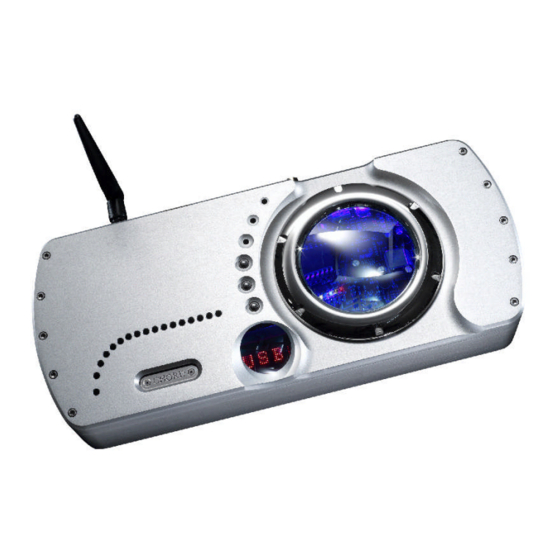
Contents Page Title page Table of Contents Input / Output connection diagram for the QBD76 Mains connection instructions Cleaning and care instructions Initial Start-up Audio Outputs Digital Input Selection Using Bluetooth wireless digital audio De-emphasis coding Setting the RAM buffer Product Specification R203WWJN000006 - 2 -... - Page 3 Chord Quarter Back DAC 76 connection diagram Display Digital input selector Output phase selector RAM buffer selector Mains power input Bluetooth antenna Word Clock output Plastic fibre optical inputs AES balanced XLR inputs 75ohm SP/DIF2 BNC Coax inputs USB input...
-
Page 4: Mains Connection Instructions
Never spray directly onto the converter and never use abrasive cleaning, use only a lint free soft cloth. There are no user serviceable parts in the QBD76. It should be serviced only by Chord Electronics Limited or their expressly approved service agents. -
Page 5: Audio Outputs
On powering the unit there should be a coloured glow from the central located glass window, the display will then scroll the word chord, then display the source that is selected, then the phase mode (positive or negative), then the level of RAM buffer selected (0BUF if RAM buffer is not in use) and then will remain displaying the input selected. -
Page 6: Setting The Ram Buffer
Setting the RAM buffer There are three settings for the RAM buffer. The options are as follows; Buffer applied Display No buffering 0BUFF Minimum buffering Maximum buffering The receiver chip takes the data from the transport and generates clocks and data in a form that the filter can accept.
Need help?
Do you have a question about the QBD 76 and is the answer not in the manual?
Questions and answers