
Related Manuals for Acrosser Technology AR-B1579


Summary of Contents for Acrosser Technology AR-B1579
-
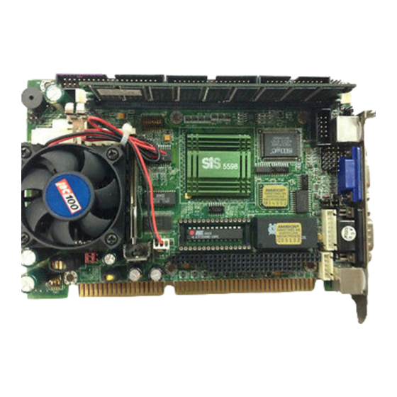
Page 1: Cpu Board
AR-B1579 Half Size Pentium(586) CPU BOARD User’s Guide Edition: 1.2 Book Number: AR-B1579... -
Page 3: Table Of Contents
AR-B1579 User's Guide Table of Contents PREFACE................................0-3 COPYRIGHT NOTICE AND DISCLAIMER......................... 0-3 WELCOME TO THE AR-B1579 CPU BOARD........................0-3 BEFORE YOU USE THIS GUIDE ............................0-3 RETURNING YOUR BOARD FOR SERVICE ........................0-3 TECHNICAL SUPPORT AND USER COMMENTS ......................0-3 ORGANIZATION................................ - Page 4 AR-B1579 User’s Guide PASSWORD SETTING ..............................5-10 5.10 LOAD DEFAULT SETTING ............................5-10 5.10.1 Auto Configuration with Optimal Setting........................ 5-10 5.10.2 Auto Configuration with Fail Safe Setting......................5-10 5.11 BIOS EXIT..................................5-10 5.11.1 Save Settings and Exit ............................5-10 5.11.2 Exit Without Saving ..............................
-
Page 5: Preface
You also could find general system information here. 0.3 BEFORE YOU USE THIS GUIDE If you have not already installed this AR-B1579, refer to the Chapter 3, “Setting Up the System,” in this guide. Check the packing list, ensure the all accessories in the package. -
Page 6: Organization
AR-B1579 User’s Guide 0.6 ORGANIZATION This information for users covers the following topics (see the Table of Contents for a detailed listing): Chapter 1, “Overview”, provides an overview of the system features and packing list. Chapter 2, “System Controller”, describes the major structure. -
Page 7: Overview
1.2 PACKING LIST The accessories are included with the system. Before you begin installing your AR-B1579 board, take a moment to make sure that the following items have been included inside the AR-B1579 package. -
Page 8: Features
AR-B1579 User’s Guide 1.3 FEATURES The system provides a number of special features that enhance its reliability, ensure its availability, and improve its expansion capabilities, as well as its hardware structure. Half size Pentium grade signal board computer Supports from 75MHz to 300MHz Pentium CPUs... -
Page 9: System Controller
Parallel Port 2.1 DMA CONTROLLER The equivalent of two 8237A DMA controllers are implemented in the AR-B1579 board. Each controller is the four- channel DMA device that will generate the memory addresses and control signals necessary to transfer information directly between a peripheral device and memory. This allows high speeding information transfer with less CPU intervention. -
Page 10: Interrupt Controller
AR-B1579 User’s Guide 2.3 INTERRUPT CONTROLLER The equivalent of two 8259 Programmable Interrupt Controllers (PIC) are included on the AR-B1579 board. They accept requests from peripherals, resolve priorities on pending interrupts in service, issue interrupt requests to the CPU, and provide vectors which are used as acceptance indices by the CPU to determine which interrupt service routine to execute. -
Page 11: I/O Port Address Map
AR-B1579 User's Guide 2.3.1 I/O Port Address Map Hex Range Device 000-01F DMA controller 1 020-021 Interrupt controller 1 022-023 SiS 5598 Chipset Address 040-04F Timer 1 050-05F Timer 2 060-06F 8042 keyboard/controller 070-071 Real-time clock (RTC), non-maskable interrupt (NMI) -
Page 12: I/O Channel Signal Description
AR-B1579 User’s Guide SA12 Input/Output -REFRESH Input/Output SA11 Input/Output BUSCLK Output SA10 Input/Output IRQ7 Input Input/Output IRQ6 Input Input/Output IRQ5 Input Input/Output IRQ4 Input Input/Output IRQ3 Input Input/Output -DACK2 Output Input/Output Output Input/Output BALE Output Input/Output Power Input/Output Output Input/Output... - Page 13 AR-B1579 User's Guide Name Description IOCHRDY This signal lengthens the I/O, or memory read/write [Input, Open collector] cycle, and should be held low with a valid address IRQ 3-7, 9-12, 14, 15 The Interrupt Request signal indicates I/O service [Input] request attention.
-
Page 14: Real-Time Clock And Non-Volatile Ram
2.3.4 Real-Time Clock and Non-Volatile RAM The AR-B1579 contains a real-time clock component that maintains the date and time in addition to storing configuration information about the computer system. It contains 14 bytes of clock and control registers and 114 bytes of general purpose RAM. -
Page 15: Serial Port
AR-B1579 User's Guide 2.4 SERIAL PORT The ACEs (Asynchronous Communication Elements ACE1 to ACE4) are used to convert parallel data to a serial format on the transmit side and convert serial data to parallel on the receiver side. The serial format, in order of transmission and reception, is a start bit, followed by five to eight data bits, a parity bit (if programmed) and one, one and half (five-bit format only) or two stop bits. - Page 16 AR-B1579 User’s Guide (5) Line Control Register (LCR) Bit 0: Word Length Select Bit 0 (WLS0) Bit 1: Word Length Select Bit 1 (WLS1) WLS1 WLS0 Word Length 5 Bits 6 Bits 7 Bits 8 Bits Bit 2: Number of Stop Bit (STB)
-
Page 17: Parallel Port
AR-B1579 User's Guide (9) Divisor Latch (LS, MS) Bit 0: Bit 0 Bit 8 Bit 1: Bit 1 Bit 9 Bit 2: Bit 2 Bit 10 Bit 3: Bit 3 Bit 11 Bit 4: Bit 4 Bit 12 Bit 5:... - Page 18 AR-B1579 User’s Guide (4) Printer Status Buffer The system microprocessor can read the printer status by reading the address of the Printer Status Buffer. The bit definitions are described as follows: -ERROR SLCT -ACK -BUSY Figure 2-2 Printer Status Buffer NOTE: X presents not used.
- Page 19 AR-B1579 User's Guide (5) Printer Control Latch & Printer Control Swapper The system microprocessor can read the contents of the printer control latch by reading the address of printer control swapper. Bit definitions are as follows: STROBE AUTO FD XT...
-
Page 21: Setting Up The System
This chapter describes pin assignments for the system’s external connectors and jumpers setting. Overview System Setting 3.1 OVERVIEW The AR-B1579 is Pentium single CPU board. This section provides hardware’s jumpers settings, connectors’ locations, and the pin assignments. Figure 3-1 External System Location... -
Page 22: System Setting
3.2.1 CRT CONNECTOR (DB1) The AR-B1579 supports CRT color monitors. It can be connected to create a compact video solution for the industrial environment. It allows a maximum CRT resolution of 1024X768. For different VGA display modes, your monitor must possess certain characteristics to display the mode you want. -
Page 23: Hard Disk (Ide) Connector
AR-B1579 User's Guide 3.2.3 Hard Disk (IDE) Connector 40-Pin Hard Disk (IDE) Connector (CN1) A 40-pin header type connector (CN1) is provided to interface with up to two embedded hard disk drives (IDE AT bus). This interface, through a 40-pin cable, allows the user to connect up to two drives in a “daisy chain” fashion. -
Page 24: Pc/104 Connector
AR-B1579 User’s Guide 3.2.4 PC/104 Connector (1) 64-Pin PC/104 Connector Bus A & B (CN8) 64-Pin PC/104 Connector -IOCHCK --- --- GND SD7 --- --- RSTDRV SD6 --- --- +5 VDC SD5 --- --- IRQ9 SD4 --- --- -5 VDC... - Page 25 AR-B1579 User's Guide (3) I/O Channel Signal Description Name Description BUSCLK [Output] The BUSCLK signal of the I/O channel is asynchronous to the CPU clock. RSTDRV [Output] This signal goes high during power-up, low line-voltage or hardware reset SA0 - SA19 The System Address lines run from bit 0 to 19.
-
Page 26: Keyboard Connector
AR-B1579 User’s Guide Name Description SBHE [Input/Output] The System Bus High Enable indicates the high byte SD8 - SD15 on the data bus -MASTER [Input] The MASTER is the signal from the I/O processor which gains control as the master and should be held low for a... -
Page 27: Fdd Port Connector (Cn2)
To use the parallel port, an adapter cable has to be connected to the CN3 (26-pin header type) connector. This adapter cable is mounted on a bracket and is included in your AR-B1579 package. The connector for the parallel port is a 25 pin D-type female connector. -
Page 28: Serial Port
AR-B1579 User’s Guide 3.2.8 Serial Port (1) RS-232/RS-485 Select (JP1, JP4 & SW1-8) JP1 selects COM B port, and adjusts the CN3 connector is RS-485 or RS-232C. JP4 selects COM A port for using DB2 for RS-232C or connects External RS-485. SW1-8 adjusts the onboard RS-485. - Page 29 (4) RS-232 Connector (CN4 & DB2) There are two serial ports with EIA RS-232C interface on the AR-B1579. COM A uses one onboard D-type 9-pin male connector (DB2) and COM B uses one 10-pin header (CN4) which are located at the right side of the card.
-
Page 30: Ps/2 Mouse Connector
To use the PS/2 interface, an adapter cable has to be connected to the J6 (6-pin header type) connector. This adapter cable is mounted on a bracket and is included in your AR-B1579 package. The connector for the PS/2 mouse is a Mini-DIN 6-pin connector. Pin assignments for the PS/2 port connector are as follows: Figure 3-19 CN5 &... -
Page 31: Power Connector (J9)
Figure 3-25 J11: Watchdog LED Header 3.2.14 CPU Setting The AR-B1579 accepts many types of 586 microprocessors such as Intel Pentium, AMD K5 & AMD K6, and Cyrix 6X86. All of these CPUs include an integer processing unit, floating-point processing unit, memory-management unit, and cache. - Page 32 AR-B1579 User’s Guide A. System Base Clock & CPU Clock Multiplier (SW1) Multiplier Clock D.O.C. RS-485 SW1 -- Factory Default Setting Figure 3-26 SW1: CPU Clock Multiplier (1) CPU Base Clock Select (SW1) This board supports different types of CPUs. The clock generator needs to be set by SW1.
- Page 33 AR-B1579 User's Guide B. CPU Logic Core Voltage Select (SW2) SW2 -- Factory Default Setting Figure 3-28 SW2: CPU Logic Core Voltage SW2-1 SW2-2 SW2-3 SW2-4 Voltage 2.16V 2.26V 2.86V 2.96V 3.36V 3.46V Table 3-7 SW2: CPU Logic Core Voltage C.
- Page 34 AR-B1579 User’s Guide AMD CPU CPU Type Work SW1-1 SW1-2 SW1-3 Frequency Clock Multiplier BF0 K5-PR75 (ABR) 75MHz 50.0MHz 1.5X 3.46V K5-PR90 (ABR) 90MHz 60.0MHz 1.5X K5-PR100 (ABR) 100MHz 66.7MHz 1.5X K5-PR120 (ABR) 90MHz 60.0MHz 1.5X K5-PR133 (ABR) 100MHz 66.7MHz 1.5X...
-
Page 35: Dram Configuration
It can assemble 16/32/64/128MB 168 pin DIMM Module Memory. When you set up 168-pin DIMM Module Memory, AR-B1579 will auto-detect DRAM, and adopt correct save order to make memory work till the best situation. Caution: Set up 168-pin DIMM Module Memory, please insert into slot vertical, if the direction is wrong and it leads to failure, please confirm the direction is right. -
Page 37: Installation
Watchdog Timer 4.1 OVERVIEW This chapter provides information for you to set up a working system based on the AR-B1579 CPU card. Please read the details of the CPU card’s hardware descriptions before installation carefully, especially jumper settings and cable connections. -
Page 38: Win 3.1 Driver
AR-B1579 User’s Guide 4.2.1 WIN 3.1 Driver For the WIN31 operating system, the user must be in DOS mode to decompress the compressed file. Make a new directory to contain the VGA drivers. Step 1: C:\>MD VGAW31 Insert the Utility Disk #1 in the floppy disk drive, and then copy the compressed file—WIN31DRV.EXE, Step 2: and the file is self-extraction program. -
Page 39: Winnt Driver
AR-B1579 User's Guide 4.2.3 WINNT Driver In the WINNT3.5 or WINNT4.0 operating system, the user must extract the compress files in DOS mode. And then setup step by step: Step 1: Make a new directory to contain the VGA drivers. -
Page 40: Watchdog Timer
This section describes how to use the Watchdog Timer, disabled, enabled, and trigger. The AR-B1579 is equipped with a programmable time-out period watchdog timer. User can use the program to enable the watchdog timer. Once you have enabled the watchdog timer, the program should trigger it every time before it times out. -
Page 41: Watchdog Transferring Select (Jp6)
AR-B1579 User's Guide If you want to generate IRQ11 signal to warn your program when watchdog times out, the following table listed the relation of timer factors between time-out period. And if you use the IRQ11 signal to warn your program when watchdog timer out, please enter the BIOS Setup the <Peripheral Setup>... -
Page 42: Watchdog Timer Disabled
AR-B1579 User’s Guide 4.3.5 Watchdog Timer Disabled To disable the watchdog timer, simply write a 00H to the watchdog register. 3000 REM Points to command register 3010 WD_REG% = BASE_PORT%+4 3020 REM Timer factor = 0 3030 TIMER_FACTOR% = 0... -
Page 43: Bios Console
BIOS Exit BIOS Update NOTE: The options of BIOS are not suitable for the AR-B1579, the settings are only fit for the AR-B1579. 5.1 BIOS SETUP OVERVIEW The BIOS is a program used to initialize and set up the I/O system of the computer, which includes the PCI bus and connected devices such as the video display, diskette drive, and the keyboard. -
Page 44: Standard Cmos Setup
AR-B1579 User’s Guide CAUTION: 1. In the AR-B1579 BIOS the factory-default setting is the <Auto Configuration with Optimal Settings> Acrosser recommends using the BIOS default settings, unless you are very familiar with the setting function, or you can contact the technical support engineer. -
Page 45: Advanced Cmos Setup
AR-B1579 User's Guide Hard Disk Setup The BIOS supports various types for user settings, The BIOS supports <Pri Master> and <Pri Slave> so the user can install up to two hard disks. For the master and slave jumpers, please refer to the hard disk’s installation descriptions and the hard disk jumper settings. - Page 46 AR-B1579 User’s Guide 1st Boot Device 2nd Boot Device 3rd Boot Device 4th Boot Device These options determine where the system looks first for an operating system. Quick Boot This category speeds up Power On Self Test (POST) after you power on the computer. If it is set to Enabled, BIOS will shorten or skip some check items during POST.
- Page 47 AR-B1579 User's Guide Wait for ‘F1’ If Error AMIBIOS POST error messages are followed by: Press <F1> to continue If this option is set to Disabled, the AMIBIOS does not wait for you to press the <F1> key after an error message.
-
Page 48: Advanced Chipset Setup
AR-B1579 User’s Guide Shadow These options control the location of the contents of the 32KB of ROM beginning at the specified memory location. If no adapter ROM is using the named ROM area, this area is made available to the local bus. The settings are:... -
Page 49: Power Management
AR-B1579 User's Guide VGA Shared Memory Size This option sets the VGA’s occupied memory size. VGA Frequency This option sets the display’s refresh. ISA Bus Clock Frequency This option sets the polling clock speed of ISA Bus (PC/104). NOTE: 1. PCLK means the CPU inputs clock. -
Page 50: Pci/Plug And Play
AR-B1579 User’s Guide Standby Time Out Suspend Time Out These options specify the length of the period of system inactivity when the computer is already in Standby mode before the computer is placed on Suspend mode. In Suspend mode, nearly all power use is curtailed. -
Page 51: Peripheral Setup
Secondary Slave Prefetch Enabled Figure 5-7 BIOS: Peripheral Setup OnBoard FDC This option enables the floppy drive controller on the AR-B1579. OnBoard Serial Port This option enables the serial port on the AR-B1579. OnBoard Parallel Port This option enables the parallel port on the AR-B1579. -
Page 52: Auto-Detect Hard Disks
AR-B1579 User’s Guide 5.8 AUTO-DETECT HARD DISKS This option detects the parameters of an IDE hard disk drive, and automatically enters them into the Standard CMOS Setup screen. 5.9 PASSWORD SETTING This BIOS Setup has an optional password feature. The system can be configured so that all users must enter a password every time the system boots or when BIOS Setup is executed. -
Page 53: Exit Without Saving
The chips can be electronically reprogrammed, allowing you to upgrade your BIOS firmware without removing and installing chips. The AR-B1579 provides FLASH BIOS update function for you to easily upgrade newer BIOS version. Please follow the operating steps for updating new BIOS: Step 1: Turn on your system and don’t detect the CONFIG.SYS and AUTOEXEC.BAT files. -
Page 55: Specifications
AR-B1579 User's Guide 6. SPECIFICATIONS CPU: Supports Pentium 75 to 300 Mhz CPU Chipset: SiS 5598 Bus Interface: PICMG PCI and non-stack through PC/104 bus RAM Memory: Supports FPM/EDO RAM, 128 MB maximum (Two 72-pin SIMMs w/o DRAM) Cache Size:... -
Page 57: Placement & Dimensions
AR-B1579 User's Guide 7. PLACEMENT & DIMENSIONS 7.1 PLACEMENT DIMM1 BUS1 BUS2... -
Page 58: Dimensions
AR-B1579 User’s Guide 7.2 DIMENSIONS 4000 1100 7−∅138 7−∅138 7−∅138 7−∅138 4150 4100 3150 1700 3000 7280 Unit: mil (1 inch = 25.4 mm = 1000 mil) -
Page 59: Programming Rs-485 & Index
Step 2: Disable TXC (transmitter control), the bit 0 of the address of offset+4 just sets “0”. NOTE: Communicates the AR-B1579 CPU card’s DTR signal with the RS-485’s TXC signal. (2) Send out one character (Transmit) Step 1: Enable TXC signal, and the bit 0 of the address of offset+4 just sets “1”. - Page 60 AR-B1579 User’s Guide (5) Basic Language Example a.) Initial 86C450 UART OPEN “COM1:9600,m,8,1”AS #1 LEN=1 REM Reset DTR OUT &H3FC, (INP(%H3FC) AND &HFA) RETURN b.) Send out one character to COM1 REM Enable transmitter by setting DTR ON OUT &H3FC, (INP(&H3FC) OR &H01)
-
Page 61: Index
2) Install SiS5598 multimedia drivers to your Windows 98. 3) Enable USB function in <Chipset Setup> item of BIOS. 4) Check whether your USB device is working properly. If you found any further problem while implementing the USB functions of AR-B1579, please contact our Customer Support for details.
Need help?
Do you have a question about the AR-B1579 and is the answer not in the manual?
Questions and answers