
Related Manuals for Acrosser Technology 386SX


Summary of Contents for Acrosser Technology 386SX
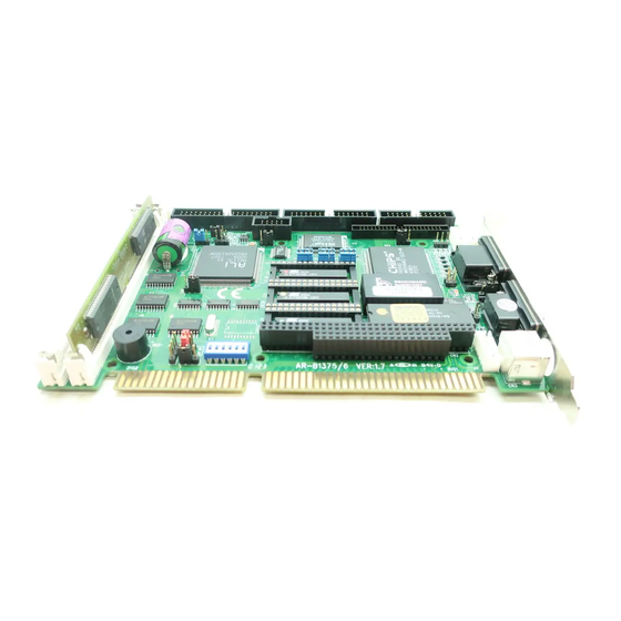
- Page 1 AR-B1375/AR-B1376 Half Size All-In-One 386SX CPU CARD User’ s Guide Edition: 1.51 Book Number: AR-B1375/AR-B1376-05.0517...
-
Page 3: Table Of Contents
Table of Contents PREFACE...0-3 COPYRIGHT NOTICE AND DISCLAIMER... 0-3 WELCOME TO THE AR-B1375/AR-B1376 CPU BOARD ... 0-3 BEFORE YOU USE THIS GUIDE... 0-3 RETURNING YOUR BOARD FOR SERVICE ... 0-3 TECHNICAL SUPPORT AND USER COMMENTS ... 0-3 ORGANIZATION ... 0-4 STATIC ELECTRICITY PRECAUTIONS ... - Page 4 AR-B1375/AR-B1376 User’s Guide SWITCH SETTING... 6-1 6.2.1 Overview ... 6-2 6.2.2 I/O Port Address Select (SW1-1) ... 6-2 6.2.3 SSD Firmware Address Select (SW1-2) ... 6-2 6.2.4 SSD Drive Number (SW1-3 & SW1-4) ... 6-3 6.2.5 ROM Type Select (SW1-5 & SW1-6) ... 6-4 JUMPER SETTING ...
-
Page 5: Preface
(C) Copyright Acrosser Technology Co., Ltd., 1997. All rights Reserved. Acrosser, ALI, AMI, PC/AT, WIN31, WIN 95, Windows NT, NEC, HITACHI, ORION, SHARP, FUJITSU, SONY, AKM, INTEL, MITSUBISHI, NS, SGS-THOMSON, TI, TOSHIBA, AMD…are registered trademarks. All other trademarks and registered trademarks are the property of their respective holders. -
Page 6: Organization
AR-B1375/AR-B1376 User’s Guide 0.6 ORGANIZATION This information for users covers the following topics (see the Table of Contents for a detailed listing): Chapter 1, “Overview,” provides an overview of the system features and packing list. Chapter 2, “System Controller,” describes the major structure. Chapter 3, “Setting Up the System,”... -
Page 7: Overview
1. OVERVIEW This chapter provides an overview of your system features and capabilities. The following topics are covered: Introduction Packing List Features 1.1 INTRODUCTION The AR-B1375 and AR-B1376 are new generation half size, 386 ISA card. This card offers much greater performance than the older cards such as support for 32MB’s of DRAM using two 72-pin SIMMs, one RS-232C/485 and one RS-232C port and 3/1.5MB solid state disk capacity for ROM, FLASH and SRAM. -
Page 8: Features
AR-B1375/AR-B1376 User’s Guide 1.3 FEATURES The system provides a number of special features that enhance its reliability, ensure its availability, and improve its expansion capabilities, as well as its hardware structure. 80386SX-33/40 MHz CPU ISA and PC/104 extension bus Up to 32MB DRAM system On-board CRT and LCD panel display (AR-B1375 doesn’t provide this function) Supports IDE hard disk drives Supports floppy disk drives... -
Page 9: System Controller
The AR-B1375 and AR-B1376 use the ALI M6117 CPU, it is designed to perform like Intel’s 386SX system with deep green features. The 386SX core is the same as M1386SX of Acer Labs. Inc. and 100% object code compatible with the Intel 386SX microprocessor. System manufacturers can provide 386 CPU based systems optimized for both cost and size. -
Page 10: Keyboard Controller
AR-B1375/AR-B1376 User’s Guide 2.3 KEYBOARD CONTROLLER The 8042 processor is programmed to support the keyboard serial interface. The keyboard controller receives serial data from the keyboard, checks its parity, translates scan codes, and presents it to the system as a byte data in its output buffer. -
Page 11: I/O Port Address Map
2.4.1 I/O Port Address Map Hex Range 000-01F 020-021 022-023 040-04F 050-05F 060-06F 070-071 080-09F 0A0-0A1 0C0-0DF 0F8-0FF 170-178 1F0-1F8 208-20A 218-21A 278-27F 2E8-2EF 2F8-2FF 300-31F 320-33F 378-37F 380-38F 3A0-3AF 3B0-3BF 3C0-3CF 3D0-3DF 3E8-3EF 3F0-3F7 3F8-3FF Table 2-2 I/O Port Address Map 2.4.2 I/O Channel Pin Assignment (Bus 1) I/O Pin Device... - Page 12 AR-B1375/AR-B1376 User’s Guide I/O Pin Table 2-3 I/O Channel Pin Assignments I/O Pin Signal Name Table 2-4 I/O Channel Pin Assignments Signal Name Input/Output I/O Pin Signal Name SA14 Input/Output SA13 Input/Output SA12 Input/Output SA11 Input/Output SA10 Input/Output Input/Output Input/Output Input/Output Input/Output Input/Output...
-
Page 13: Real-Time Clock And Non-Volatile Ram
2.5 REAL-TIME CLOCK AND NON-VOLATILE RAM The AR-B1375/AR-B1376 contains a real-time clock compartment that maintains the date and time in addition to storing configuration information about the computer system. It contains 14 bytes of clock and control registers and 114 bytes of general purpose RAM. Because of the use of CMOS technology, it consumes very little power and can be maintained for long period of time using an internal Lithium battery. -
Page 14: Serial Port
AR-B1375/AR-B1376 User’s Guide 2.7 SERIAL PORT The ACEs (Asynchronous Communication Elements ACE1 to ACE4) are used to convert parallel data to a serial format on the transmit side and convert serial data to parallel on the receiver side. The serial format, in order of transmission and reception, is a start bit, followed by five to eight data bits, a parity bit (if programmed) and one, one and half (five-bit format only) or two stop bits. - Page 15 (5) Line Control Register (LCR) Bit 0: Word Length Select Bit 0 (WLS0) Bit 1: Word Length Select Bit 1 (WLS1) WLS1 WLS0 Bit 2: Number of Stop Bit (STB) Bit 3: Parity Enable (PEN) Bit 4: Even Parity Select (EPS) Bit 5: Stick Parity Bit 6: Set Break Bit 7: Divisor Latch Access Bit (DLAB)
-
Page 16: Parallel Port
AR-B1375/AR-B1376 User’s Guide (9) Divisor Latch (LS, MS) Bit 0: Bit 0 Bit 1: Bit 1 Bit 2: Bit 2 Bit 3: Bit 3 Bit 4: Bit 4 Bit 5: Bit 5 Bit 6: Bit 6 Bit 7: Bit 7 Desired Baud Rate 134.5... - Page 17 (4) Printer Status Buffer The system microprocessor can read the printer status by reading the address of the Printer Status Buffer. The bit definitions are described as follows: NOTE: X presents not used. Bit 7: This signal may become active during data entry, when the printer is off-line during printing, or when the print head is changing position or in an error state.
-
Page 19: Setting Up The System
3. SETTING UP THE SYSTEM This section describes pin assignments for system’s external connectors and the jumpers setting. Overview System Setting 3.1 OVERVIEW The AR-B1375 and AR-B1376 are all-in-one half size, Pentium single CPU board. hardware’s jumpers setting, the connectors’ locations, and the pin assignment. CAUTION: The CPU board doesn’t support the type DRAM SIMM of two-sided, it only supports single side DRAM SIMM. -
Page 20: System Setting
AR-B1375/AR-B1376 User’s Guide 3.2 SYSTEM SETTING Jumper pins allow you to set specific system parameters. Set them by changing the pin location of jumper blocks. (A jumper block is a small plastic-encased conductor [shorting plug] that slips over the pins.) To change a jumper setting, remove the jumper from its current location with your fingers or small needle-nosed pliers. -
Page 21: Pc/104 Connector
3.2.2 PC/104 Connector (1) 40-Pin PC/104 Connector Bus C & D (CN1) Figure 3-4 CN1: 40-Pin PC/104 Connector Bus C & D Figure 3-5 CN1: 40-Pin PC/104 Connector Bus C & D (2) 64-Pin PC/104 Connector Bus A & B (CN2) Figure 3-6 CN2: 64 Pin PC/104 Connector Bus A &... - Page 22 AR-B1375/AR-B1376 User’s Guide (3) I/O Channel Signal Description Name BUSCLK [Output] RSTDRV [Output] SA0 - SA19 [Input / Output] LA17 - LA23 [Input/Output] SD0 - SD15 [Input/Output] BALE [Output] -IOCHCK [Input] IOCHRDY [Input, Open collector] IRQ 3-7, 9-12, 14, 15 -IOR [Input/Output] -IOW [Input/Output]...
-
Page 23: Hard Disk (Ide) Connector (Cn4)
Name -MASTER [Input] -MEMCS16 [Input, Open collector] -IOCS16 [Input, Open collector] OSC [Output] -ZWS [Input, Open collector] Table 3-9 I/O Channel Signal’s Description 3.2.3 Hard Disk (IDE) Connector (CN4) A 40-pin header type connector (CN4) is provided to interface with up to two embedded hard disk drives (IDE AT bus). -
Page 24: Fdd Port Connector (Cn5)
AR-B1375/AR-B1376 User’s Guide 3.2.4 FDD Port Connector (CN5) The AR-B1375 and AR-B1376 provide a 34-pin header type connector for supporting up to two floppy disk drives. 1-33(odd) Table 3-1 FDD Pin Assignment 3.2.5 Parallel Port Connector (CN6) To use the parallel port, an adapter cable has connected to the CN6 (26-pin header type) connector. This adapter cable is mounted on a bracket and is included in your AR-B1375 or AR-B1376 package. -
Page 25: Serial Port
3.2.6 Serial Port (1) RS-232/RS-485 Select for COM-B (JP2) JP2 select the on-board RS-232/RS-485 for COM B, if choose RS-232 connecting with CN7; if choose RS-485 connecting with J9. Figure 3-11 JP2: RS-232/RS-485 Select for COM-B (2) RS-485 Terminator (JP7) (3) External RS-485 Adapter Select (J6 &... -
Page 26: Reset Header (J1)
AR-B1375/AR-B1376 User’s Guide (5) RS-232 Connector (CN7 & DB2) There are two serial ports with EIA RS-232 interface on the AR-B1375 or AR-B1376. COM A uses one on-board D-type 9-pin male connector (DB2) which is located at the right side of the card, and COM B uses one 10-pin header (CN7) which is located at the upper of the card. -
Page 27: Power Connector (J3)
(3) Watchdog LED Header (J10) 3.2.9 Power Connector (J3) J3 is 8-pin power connector, you can directly connect the power supply to the on board power connector for stand alone applications. 3.2.10 External Speaker Header (J5) Besides the on board buzzer, you can use an external speaker by connecting J5 header directly. 3.2.11 External Battery (1) Battery Charger Select (JP3) LED+... -
Page 28: Cpu Base Clock Select (Jp1)
AR-B1375/AR-B1376 User’s Guide (2) External Battery Connector (J11) J11 allows users to connector an external 4.5 to 6 VDC battery to the AR-B1375 and AR-B1376 if the on-board battery is fully discharged. The SRAM disk will draw the battery current. The battery charger on AR-B1375 and AR-B1376 doesn’t source charge current to the external battery, which connects to J11. -
Page 29: Crt/Lcd Flat Panel Display
4. CRT/LCD FLAT PANEL DISPLAY This section describes the configuration and installation procedure using LCD and CRT display. Connecting the CRT Monitor LCD Flat Panel Display Supported LCD Panel 4.1 CONNECTING THE CRT MONITOR 4.1.1 VGA Setting (JP5) (1) IRQ 9 Used Select (2) Zero Wait State JP5:Pin 1-2 Selecting IRQ 9 Disabled... -
Page 30: Crt Connector (Cn13)
AR-B1375/AR-B1376 User’s Guide 4.1.2 CRT Connector (DB1) DB1 is used to connect with a VGA monitor when you are using the on-board VGA controller as display adapter. Pin assignments for the DB1 connector is as follows: NOTE: DB1 on the AR-B1375 is not functional. Its function is always used on the AR-B1376 CPU board. 4.2 LCD FLAT PANEL DISPLAY This section describes the configuration and installation procedure for a LCD display. -
Page 31: Inverter Board Description
NOTE: Be careful with the pin orientation when installing connectors and the cables. A wrong connection can easily destroy your LCD panel. Pin 1 of the cable connector is indicated with a sticker and pin1 of the ribbon cable is usually has a different color. 4.2.1 Inverter Board Description The inverter board is the one that supplies the high voltage signals to drive the LCD panel by converting the 12 volt signal from the AR-B1376 into high voltage AC signal for LCD panel. -
Page 32: Supported Lcd Panel
AR-B1375/AR-B1376 User’s Guide (3) LCD Panel Display Connector (CN8) Attach a display panel connector to this 44-pin connector with pin assignments as shown below: NOTE: AR-B1375 doesn’t provide this function. Table 4-4 LCD Display Assignment 4.3 SUPPORTED LCD PANEL At present, this VGA card can provide a solution with an inverter board for the following list of standard LCD panels. -
Page 33: Installation
5. INSTALLATION This chapter describes the procedure of the utility diskette installation. The following topics are covered: Overview Utility Diskette Write Protect Function Watchdog Timer 5.1 OVERVIEW This chapter provides information for you to set up a working system based on the AR-B1375/AR-B1376 CPU card. Please read the details of the CPU card’s hardware descriptions before installation carefully, especially jumpers’... -
Page 34: Vga Driver
AR-B1375/AR-B1376 User’s Guide 5.2.1 VGA Driver (1) WIN 3.1 Driver For the WIN31 operation system, user must in the DOS mode decompress the compress file. And then as to the steps: In the DOS mode execute the SETUP.EXE file. Step 1: A:\>SETUP The screen shows the chip type, and press any key enter the main menu. -
Page 35: Ssd Utility
5.2.2 SSD Utility To support the AR-B1375/AR-B1376 solid-state disk’s operations, the following files have been provided on the enclosed diskette’s directory <SSD>. (A) PGM137x.EXE PGM137x.EXE PGM137x.EXE is used to program the 12V FLASH EPROM after the ROM pattern files are generated by RFG.EXE. - Page 36 AR-B1375/AR-B1376 User’s Guide (C) WP137x.EXE WP137x.EXE This program demonstrates how to enable and disable software write protected function. It also shows the current protect mode of write or read only memory. (D) RFG.EXE RFG.EXE This program is used to generate ROM pattern files in a binary format. Each ROM pattern file has the same size as the FLASH or EPROM and can be easily programmed on to the FLASH with on-board programmer or on to EPROM with any EPROM programmer.
-
Page 37: Write Protect Function
(E) RFGDEMO.PGF RFGDEMO.PGF This file provides a sample PROGRAM GROUP FILE, which illustrates how to create ROM pattern files correctly. The PGF is an ASCII text file that can be created by using any text editor, word processor or DOS <COPY CON> command. -
Page 38: Hardware Write Protect
AR-B1375/AR-B1376 User’s Guide 5.3.1 Hardware Write Protect To enable the hardware protect function for small page 5V FLASH disk, please refer to the “Switch Setting”. 5.3.2 Software Write Protect If you need the write protect function and sometimes you have to write or update data on your FLASH/SRAM disk, you can use the software write protect instead of hardware write protect. -
Page 39: Watchdog Timer
5.4 WATCHDOG TIMER This section describes how to use the Watchdog Timer, disabled, enabled, and trigger. The AR-B1375/AR-B1376 is equipped with a programmable time-out period watchdog timer. User can use the program to enable the watchdog timer. Once you have enabled the watchdog timer, the program should trigger it every time before it times out. -
Page 40: Watchdog Timer Enabled
AR-B1375/AR-B1376 User’s Guide NOTE: 1. If you program the watchdog to generate IRQ15 signal when it times out, you should initial IRQ15 interrupt vector and enable the second interrupt controller (8259 PIC) in order to enable CPU to process this interrupt. An interrupt service routine is required too. 2. -
Page 41: Solid State Disk
6.SOLID STATE DISK The section describes the various type SSDs’ installation steps as follows. This chapter describes the procedure of the installation. The following topics are covered: Overview Switch Setting Jumper Setting ROM Disk Installation 6.1 OVERVIEW The AR-B1375 and AR-B1376 provides three 32-pin JEDEC DIP sockets, which may be populated with up to 3MB of EPROM or 1.5MB of FLASH or 1.5MB of SRAM disk. -
Page 42: Overview
AR-B1375/AR-B1376 User’s Guide 6.2.1 Overview There is 1 DIP Switch located on the AR-B1375 and AR-B1376. It performs the following functions: SW1-1 SW1-2 SW1-3 & SW1-4 Set the drive number of solid state SW1-5 & SW1-6 Set the used ROM memory chips 6.2.2 I/O Port Address Select (SW1-1) SW1-1 is provided to select one of the four base port addresses for the watchdog timer and the solid state disk. -
Page 43: Ssd Drive Number (Sw1-3 & Sw1-4)
6.2.4 SSD Drive Number (SW1-3 & SW1-4) The AR-B1375/AR-B1376’s SSD can simulate one or two disk drives. You can assign the drive letter of the AR- B1375/AR-B1376 by configuring SW1-3 & SW1-4. You can make the computer to boot from SSD by copying DOS into the SSD. If your SSD does not have DOS, the computer will boot from your hard disk or floppy disk. -
Page 44: Rom Type Select (Sw1-5 & Sw1-6)
AR-B1375/AR-B1376 User’s Guide (2) Disk Drive Name Arrangement If any logical hard disk drives exist in your system, there will also be a different disk number depending on which version DOS you are using. The solid state disk drive number with there respective DOS drive designation are listed in table as follows. The solid state disk drive number is changeable as the DOS version. -
Page 45: Jumper Setting
6.3 JUMPER SETTING Before installing the memory into memory sockets MEM1 through MEM3 (U31, U32 and U33 respectively), you have to configure the memory type which will be used (ROM/RAM) on the AR-B1375 and AR-B1376. Each socket is equipped with an jumper to select the memory type. You can configure the AR-B1375 and AR-B1376 as a (FLASH) EPROM disk (ROM only), a SRAM disk (SRAM only) or a combination of (FLASH) EPROM and SRAM disk. -
Page 46: Rom Disk Installation
AR-B1375/AR-B1376 User’s Guide 6.4 ROM DISK INSTALLATION The section describes the various type SSDs’ installation steps as follows. The jumper and switch adjust as SSD’s different type to set. 6.4.1 UV EPROM (27Cxxx) (1) Switch and Jumper Setting Step 1: Use jumper block to set the memory type as ROM (FLASH). Step 2: Select the proper I/O base port, firmware address, disk drive number and EPROM type on SW1. -
Page 47: Large Page 5V Flash Disk
(2) Software Programming Use the UV EPROM, please refer to the follow steps: Step 1: Turn on the power and boot DOS from hard disk drive or floppy disk drive. Step 2: Making a Program Group File (*.PGF file) Step 3: Using the RFG.EXE to generate ROM pattern files, and counting the ROM numbers as the pattern files. - Page 48 AR-B1375/AR-B1376 User’s Guide (2) Software Programming And then, you should create a PGF and generate ROM pattern files by using the RFG.EXE. Step 1: Making a Program Group File (*.PGF file) Step 2: Generate ROM pattern files Turn off your system, and then install FLASH EPROMs into the sockets. Step 3: NOTE: Place the appropriate number of FLASH EPROM chips (the numbers depends on the ROM pattern files generated by RFG.EXE) into the socket starting from MEM1 and ensure that the...
-
Page 49: Small Page 5V Flash Rom Disk
6.4.3 Small Page 5V FLASH ROM Disk (1) Switch and Jumper Setting Step 1: Use jumper block to set the memory type as ROM (FLASH). Step 2: Select the proper I/O base port, firmware address, disk drive number and EPROM type on SW1. Step 3: Insert programmed EPROM(s) or FLASH(s) chips into sockets starting at MEM1. -
Page 50: Ram Disk
AR-B1375/AR-B1376 User’s Guide (3) Typing DOS Command You can use another way to format and copy files to the 5V FLASH EPROM. convenience of using a RAM disk. You can use the DOS <FORMAT> and <COPY> command to format and copy files. -
Page 51: Combination Of Rom And Ram Disk
(2) Software Programming It is very easy to use the RAM disk. The RAM disk operates just like a normal floppy disk. A newly installed RAM disk needs to be formatted before files can be copied to it. Use the DOS command [FORMAT] to format the RAM disk. -
Page 53: Bios Console
7. BIOS CONSOLE This chapter describes the AR-B1375/AR-B1376 BIOS menu displays and explains how to perform common tasks needed to get up and running, and presents detailed explanations of the elements found in each of the BIOS menus. The following topics are covered: BIOS Setup Overview Standard CMOS Setup Advanced CMOS Setup... -
Page 54: Standard Cmos Setup
AR-B1375/AR-B1376 User’s Guide 7.2 STANDARD CMOS SETUP The <Standard CMOS Setup> option allows you to record some basic system hardware configuration and set the system clock and error handling. If the CPU board is already installed in a working system, you will not need to select this option anymore. -
Page 55: Advanced Cmos Setup
7.3 ADVANCED CMOS SETUP The <Advanced CMOS SETUP> option consists of configuration entries that allow you to improve your system performance, or let you set up some system features according to your preference. Some entries here are required by the CPU board ’ s design to remained in their default settings. - Page 56 AR-B1375/AR-B1376 User’s Guide System Keyboard This function specifies that a keyboard is attached to the computer. Primary Display The option is used to set the type of video display card installed in the system. Password Check This option enables password checking every time the computer is powered on or every time the BIOS Setup is executed.
-
Page 57: Advanced Chipset Setup
OnBoard FDC This option enables the floppy drive controller on the AR-B1375 and AR-B1376. OnBoard Serial Port This option enables the serial port on the AR-B1375 and AR-B1376. OnBoard Parallel Port This option enables the parallel port on the AR-B1375 and AR-B1376. Parallel Port Mode This option specifies the parallel port mode. -
Page 58: Password Setting
AR-B1375/AR-B1376 User’s Guide Time Insert Wait The DRAM time insert wait: RAS Active and CAS Precharge function setting. Memory Write Insert Wait ISA bus memory write insert wait ISA High Speed The Speed field shows the speed at which the processor runs internally. I/O Recovery If I/O Recovery Feature options is enabled, the BIOS inserts a delay time between two I/O commands. -
Page 59: Auto Configuration With Fail Safe Setting
7.6.2 Auto Configuration with Fail Safe Setting User can load the Fail-Safe BIOS Setup option settings by selecting the Fail-Safe item from the Default section of the BIOS Setup main menu. The Fail-Safe settings provide far from optimal system performance, but are the most stable settings. Use this option as a diagnostic aid if the system is behaving erratically. - Page 60 AR-B1375/AR-B1376 User’s Guide Flash EPROM Programming is going to start. System will not be usable until Programming of Flash EPROM is successfully complete. In case of any error, existing Flash EPROM must be replaced by new program Flash EPROM. As the gray statement, press the <Y> key to updating the new BIOS. Step 6: And then the <Message>...
-
Page 61: Specifications & Ssd Types Supported
8. SPECIFICATIONS & SSD TYPES SUPPORTED 8.1 SPECIFICATIONS ALI M6117, 33/40 MHz CPU & Chipset: ISA and PC/104 bus Bus Interface: Supports up to 32MB (two 72-pin SIMMs) DRAM: CRT/LCD Display: 1 MB RAM (1024X768/256 colors) with 10-pin and 44-pin header Supports two IDE type hard disk drives HDC: Supports two 5.25”... - Page 62 The following list contains small page 5V FLASHs supported by the AR-B1375/AR-B1376: ATMEL ATMEL WINBOND ATMEL ATMEL ATMEL The following list contains EPROMs supported by the AR-B1375/AR-B1376: ATMEL FUJITSHU HITACHI INTEL MITSHUBISHI SGS-THOMSON TOSHIBA ATMEL FUJITSU HITACHI INTEL MITSHUBISHI SGS-THOMSON TOSHIBA ATMEL FUJITSU HITACHI INTEL MITSUBISHI SGS-THOMSON...
-
Page 63: Using Memory Banks
9. USING MEMORY BANKS This appendix provides the information about how to access the memory on the AR-B1375 and AR-B1376 without using the AR-B1375 and AR-B1376 SSD BIOS. The AR-B1375 and AR-B1376 hardware divides every 8K bytes of memory into a memory bank. To access the data in the memory, you have to assign the chip number and the bank number. -
Page 65: Placement & Dimensions
10. PLACEMENT & DIMENSIONS 10.1 PLACEMENT H11 H10 BUS2 LED2 P5 P3 P1 P6 P4 P2 A B C A B C MEM1 MEM2 MEM3 BUS1 AR-B1375/AR-B1376 User’s Guide LED1 A B C LED3 10-1... -
Page 66: Dimensions
AR-B1375/AR-B1376 User’s Guide 10.2 DIMENSIONS 10-2 7−∅58 1700 7280 Unit: mil (1 inch = 25.4 mm = 1000 mil) 4000 1100 4150 4100 1000 3000... -
Page 67: Programming Rs-485 & Index
11. PROGRAMMING RS-485 & INDEX 11.1 PROGRAMMING RS-485 The majority communicative operation of the RS-485 is in the same of the RS-232. When the RS-485 proceeds the transmission which needs control the TXC signal, and the installing steps are as follows: Enable TXC Step 1: Send out data... - Page 68 AR-B1375/AR-B1376 User’s Guide (5) Basic Language Example a.) Initial 86C450 UART OPEN “COM1:9600,m,8,1”AS #1 LEN=1 REM Reset DTR OUT &H3FC, (INP(%H3FC) AND &HFA) RETURN b.) Send out one character to COM1 REM Enable transmitter by setting DTR ON OUT &H3FC, (INP(&H3FC) OR &H01) REM Send out one character PRINT #1, OUTCHR$ REM Check transmitter holding register and shift register...
-
Page 69: Index
11.2 INDEX Name SIMM1 SIMM2 M1~M3 NOTE: * presents AR-B1375 does not provide these functions. Note: If the content in Setting is inconsistent with the CD-ROM. Please refer to the Setting as priority. Function 40 pin PC/104 connector bus C & D 64 pin PC/104 connector bus A &...
Need help?
Do you have a question about the 386SX and is the answer not in the manual?
Questions and answers