Table of Contents
Advertisement
Quick Links
Advertisement
Table of Contents

Subscribe to Our Youtube Channel
Related Manuals for BBK BBK916S


Summary of Contents for BBK BBK916S
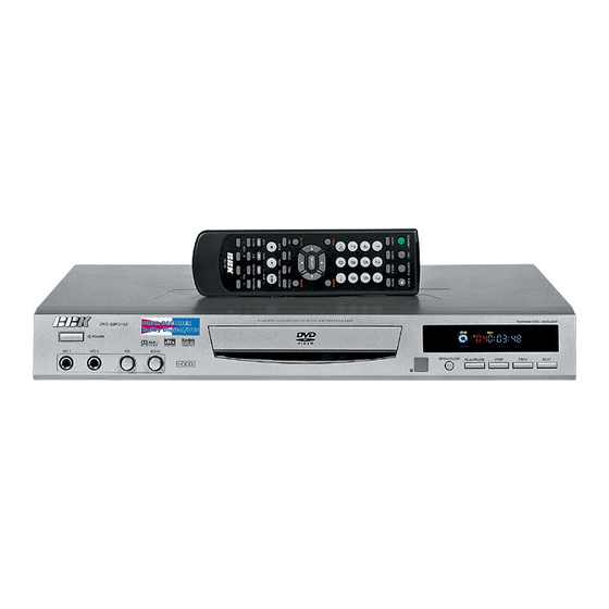
- Page 1 SERVICE MANUAL BBK916S...
-
Page 2: Table Of Contents
CONTENTS SAFETY PRICAUTIONS PREVENTION OF ELECTRO STATIC DISCHARGE(ESD)TO ELECTROSTATICALLY SENSITIVE(ES)DEVICES CONTROL BUTTON LOCATIONS AND EXPLANATIONS PREVERTION OF STATIC ELECTRICITY DISCHARGE ASSEMBLING AND DISASSEMBLING THE MECHANISM UNIT OPTICAL PICKUP UNIT INSTALLATION CHAT BRACKET INSTALLATION CHART MISCELLANEOUS ELECTRICAL CONFIRMATION VIDEO OUTPUT (LUMINANCE SIGNAL) CONFIRMATION VIDEO OUTPUT(CHROMINANCE SIGNAL) CONFIRMATION MPEG BOARD CHECK WAVEFORM IC BLOCK DIAGRAM &... -
Page 3: Safety Pricautions
1. SAFETY PREAUTIONS 1.1 GENERAL GUIDELINES 1. When servicing, observe the original lead dress. if a short circuit is found, replace all parts which have been overheated or damaged by the short circuit. 2. After servicing, see to it that all the protective devices such as insulation barrier, insulation papers shields are properly installed. - Page 5 STANDBY Button Press once to stand by, Press twice to play. OSD Button Display or hid disc information. GOTO Button Play from the desired location. AUDIO Button Change the audio language or audio channel. EJECT Button Open or close the disc tray.
-
Page 6: Prevention Of Static Electricity Discharge
4.PREVENTION OF STATIC ELECTRICITY DISCHARGE The laser diode in the traverse unit (optical pickup)may brake down due to static electricity of clothes or human body. Use due caution to electrostatic breakdown when servicing and handling the laser diode. 4.1.Grounding for electrostatic breakdown prevention Some devices such as the DVD player use the optical pickup(laser diode)and the optical pickup will be damaged by static electricity in the working environment.Proceed servicing works under the working environment where grounding works is completed. -
Page 7: Assembling And Disassembling The Mechanism Unit
5. Assembling and disassembling the mechanism unit 5.1 Optical pickup Unit Explosed View and Part List Pic (1) - Page 8 Materials to Pic (1) PARTS CODE PARTS NAME Q ty 14692200 SF-HD60 1EA0311A06300 ASSY, CHASSIS, COMPLETE 1EA0M10A15500 ASSY, MOTOR, SLED 1EA0M10A15501 ASSY, MOTOR, SLED 1EA2451A24700 HOLDER, SHAFT 1EA2511A29100 GEAR, RACK 1EA2511A29200 GEAR, DRIVE 1EA2511A29300 GEAR, MIDDLE, A 1EA2511A29400 GEAR, MIDDLE, B 1EA2744A03000 SHAFT, SLIDE 1EA2744A03100...
-
Page 9: Bracket Installation Chart
5.2 Bracket Explosed View and Part List Pic (2) Materials to Pic(2) 1.bracket 14. front silicon rubber 2.belt 15. Back silicon rubber 3.screw 16. Pick-up 4.belt wheel 17. Pick-up 5.gearwheel 18. switch 6.iron chip 19. Five-pin flat plug 7. Immobility mechanism equipment 20. -
Page 10: Miscellaneous
5.3 MISCELLANEOUS 5.3.1 Protection of the LD(Laser diode) Short the parts of LD circuit pattern by soldering. 5.3.2 Cautions on assembly and adjustment Make sure that the workbenches,jigs,tips,tips of soldering irons and measuring instruments are grounded,and that personnel wear wrist straps for ground. Open the LD short lands quickly with a soldering iron after a circuit is connected. -
Page 11: Electrical Confirmation
6.Electrical Confirmation 6.1. Video Output (Luminance Signal) Confirmation DO this confirmation after replacing a P.C.B. Measurement point Mode Disc Color bar 75% DVDT-S15 Video output terminal PLAY(Title 46):DVDT-S15 PLAY(Title 12):DVDT-S01 DVDT-S01 Measuring equipment,tools Confirmation value 200mV/dir,10 sec/dir 1000mVp-p±30mV Purpose:To maintain video signal output compatibility. 1.Connect the oscilloscope to the video output terminal and terminate at 75 ohms. -
Page 12: Video Output(Chrominance Signal) Confirmation
6.2 Video Output(Chrominance Signal) Confirmation Do the confirmation after replacing P.C.B. Measurement point Mode Disc Color bar 75% DVDT-S15 Video output terminal PLAY(Title 46):DVDT-S15 PLAY(Title 12):DVDT-S01 DVDT-S01 Measuring equipment,tools Confirmation value Screwdriver,Oscilloscope 200mV/dir,10 sec/dir 621mVp-p±30mV Purpose:To maintain video signal output compatibility. 1.Connect the oscilloscope to the video output terminal and terminate at 75 ohme. -
Page 13: Mpeg Board Check Waveform
7.MPEG BOARD CHECK WAVEFORM 7.1 27MHz WAVEFORM DIAGRAM 7.2 IC5L0380R PIN.2 WAVEFORM DIAGRAM... -
Page 14: Ic Block Diagram & Description
MT1336 PRELIMINARY, SUBJ ECT TO CHANGE WITHOUT NOTICE MTK CONFIDENTIAL, NO DISCLOSURE 8. IC BLOCK DIAGRAM & DESCRIPTION 8.1 MT1336 GENERAL DESCRIPTION M T 1 3 3 6 i s a h i g h p e r f o r m a n c e C M O S a n a l o g f r o n t -e n d I C f o r b o t h C D _ R O M d r i v e r u p t o 4 8 X S a n d D V D - R O M d r i v e r u p t o 1 6 X S . - Page 15 MT1336 PRELIMINARY, SUBJ ECT TO CHANGE WITHOUT NOTICE MTK CONFIDENTIAL, NO DISCLOSURE DVDA RFOP DVDB ATTENUATOR INPUT MUX RFON DVDC LRFRP DEFECT DVDD HRFRP CRTP DVDRFIN ENVELOP ENVELOP CRTPLP DETECTOR DETECTOR DVDRFIP REFCOS HALLCOS SBAD COSPHI DPFN REFSIN DPFO HALLSIN SINPHI DPDMUTE MDI2...
- Page 16 MT1336 PRELIMINARY, SUBJ ECT TO CHANGE WITHOUT NOTICE MTK CONFIDENTIAL, NO DISCLOSURE W O BSO W V D D A G N D X DVDA A G N D X DVDB A V D D O DVDC R FO P DVDD R FO N DVDRFI P...
- Page 17 MT1336 PRELIMINARY, SUBJ ECT TO CHANGE WITHOUT NOTICE MTK CONFIDENTIAL, NO DISCLOSURE MT1336 PIN DESCRIPTIONS Pin Numbers Symbol Type Description LQFP128 RF Flag Interface DEFECT Digital Output Flag of bad data output status RF SIO interface SCLK Digital Input RF serial clock input SDEN Digital Input RF serial data enable...
- Page 18 MT1336 PRELIMINARY, SUBJ ECT TO CHANGE WITHOUT NOTICE MTK CONFIDENTIAL, NO DISCLOSURE RFGCU Analog RF AGC loop capacitor connecting for DVD -RAM RFGCI Analog RF AGC loop capacitor connecting for DVD -RAM Analog Input DC coupled DVD-RAM main-beam RF signal input A Analog Input DC coupled DVD-RAM main-beam RF signal input B Analog Input...
- Page 19 MT1336 PRELIMINARY, SUBJ ECT TO CHANGE WITHOUT NOTICE MTK CONFIDENTIAL, NO DISCLOSURE Analog Input MDI1 Laser power monitor input LDO1 Analog Ou tput Laser driver output Analog Input MDI2 Laser power monitor input LDO2 Analog Output Laser driver output RF RIPPLE CRTP Analog RF top envelop filter capacitor connecting...
- Page 20 MT1336 PRELIMINARY, SUBJ ECT TO CHANGE WITHOUT NOTICE MTK CONFIDENTIAL, NO DISCLOSURE ALPC TRIMMING Analog input Trimming pin for ALPC1 Analog input Trimming pin for ALPC1 Analog input Trimming pin for ALPC2 Analog input Trimming pin for ALPC2 HIGH SPEED TRACK COUNTING TRLP Analog Low-pass filter capacitor connecting...
- Page 21 MT1336 PRELIMINARY, SUBJ ECT TO CHANGE WITHOUT NOTICE MTK CONFIDENTIAL, NO DISCLOSURE...
-
Page 22: Mt1369
MT1369 DVD Player Combo Chip Specifications are subject to change without notice 8.2 MT1369 EATURES § Built-in 8032 micro controller Super Integration DVD player single chip § Built-in internal 373 and 8-bit programmable § Servo controller and data channel processing lower address port §... - Page 23 MT1369 PRELIMINARY, SUBJECT TO CHANGE WITHOUT NOTICE MTK CONFIDENTIAL, NO DISCLOSURE Video Decode - MLP decoding for DVD -Audio § Decodes MPEG1 video and MPEG2 main level, - MPEG-1 layer 1/layer 2 audio decoding main profile video (720/480 and 720x576) - MPEG-2 layer1/layer2 2 -channel audio decoding §...
- Page 24 MT1369 PRELIMINARY, SUBJECT TO CHANGE WITHOUT NOTICE MTK CONFIDENTIAL, NO DISCLOSURE EFINITIONS Symbol Type Description IREF Analog Input Current reference input. It generate reference current for data PLL. Connect an external 100K resistor to this pin and PLLVSS. PLLVSS Ground Ground for data PLL and related analog circuitry LPIOP Analog Output...
- Page 25 MT1369 PRELIMINARY, SUBJECT TO CHANGE WITHOUT NOTICE MTK CONFIDENTIAL, NO DISCLOSURE Symbol Type Description IOA2 Inout, Pull Up Microcontroller address 2 / GPIO2 IOA3 Inout, Pull Up Microcontroller address 3 / GPIO3 IOA4 Inout, Pull Up Microcontroller address 4 / GPIO4 IOA5 Inout, Pull Up Microcontroller address 5 / GPIO5...
- Page 26 MT1369 PRELIMINARY, SUBJECT TO CHANGE WITHOUT NOTICE MTK CONFIDENTIAL, NO DISCLOSURE Symbol Type Description RWE# Output DRAM write enable, active low CAS# Output DRAM column address strobe, active low RAS# Output DRAM row address strobe, active low RCS# Output DRAM chip select, active low Output DRAM bank address 0 DVDD3...
- Page 27 MT1369 PRELIMINARY, SUBJECT TO CHANGE WITHOUT NOTICE MTK CONFIDENTIAL, NO DISCLOSURE Symbol Type Description RD27 Inout, Pull Up/Down DRAM data 27 RD26 Inout, Pull Up/Down DRAM data 26 RD25 Inout, Pull Up/Down DRAM data 25 RD24 Inout, Pull Up/Down DRAM data 24 DVSS Ground Ground...
- Page 28 MT1369 PRELIMINARY, SUBJECT TO CHANGE WITHOUT NOTICE MTK CONFIDENTIAL, NO DISCLOSURE Symbol Type Description VFO13 Output The 1st, 3rd VFO pulse output of DVD-RAM ID header IDGATE Output DVD-RAM ID header detect signal output DVDD3 Power 3.3V power UDGATE Output DVD-RAM recording data gate signal output WOBSI Input...
- Page 29 MT1369 PRELIMINARY, SUBJECT TO CHANGE WITHOUT NOTICE MTK CONFIDENTIAL, NO DISCLOSURE IREF APVDD3 PLLVSS ACLK LPIOP ASDATA2 LPION ASDATA1 LPFON ASDATA0 LPFIP DVDD3 LPFIN ALRCK LPFOP ABCK JITFO RD16 JITFN RD17 PLLVDD3 DVSS RD18 RD19 TROPENPWM RD20 PWMOUT2 RD21 DVDD2 DVDD2 RD22 RD23...
- Page 30 MT1369 PRELIMINARY, SUBJECT TO CHANGE WITHOUT NOTICE MTK CONFIDENTIAL, NO DISCLOSURE UNCTIONAL LOCK T V e n c o d e r D V D m o d u l e S e r v o A n a l o g S p i n d l e D e b u g S y s t e m...
- Page 31 MT1369 PRELIMINARY, SUBJECT TO CHANGE WITHOUT NOTICE MTK CONFIDENTIAL, NO DISCLOSURE The spindle controller is used to control disc spindle motor. It includes a varipitch CLV clock generator, a CLV/CAV controller, and a PWM generator. The varipitch CLV clock enerator generates a reference colck for the speed of operation. The CLV/CAV controller changes the mode and speed of operation according to servo register setting.
- Page 32 MT1369 PRELIMINARY, SUBJECT TO CHANGE WITHOUT NOTICE MTK CONFIDENTIAL, NO DISCLOSURE The Video Processor unit integrates two separate horizontal postprocessing filter, a simple 2-tap linear horizontal filter and an 8-tap programmable filter. These filters are prov ided for scaling images horizontally along the scan line. These two filters is capable of generating up to eight, unique subpixel values between two consecutive pixels on a scan line.
-
Page 33: U214 Hy29F800
IC BLOCK DIAGRAM & DESCRIPTION 8.3 U214 HY29F800 KEY FEATURES n Sector Protection n 5 Volt Read, Program, and Erase – Minimizes system-level power requirements – Any combination of sectors may be n High Performance locked to prevent program or erase –... -
Page 34: Block Diagram
IC BLOCK DIAGRAM & DESCRIPTION BLOCK DIAGRAM DQ[15:0] A[18:0], A-1 STATE C O N T R O L ERASE VOLTAGE I/O BUFFERS G E N E R A T O R A N D DQ[15:0] S E C T O R S W I T C H E S C O M M A N D W E # REGISTER... - Page 35 IC BLOCK DIAGRAM & DESCRIPTION PIN CONFIGURATIONS RY/BY# RESET# W E # BYTE# DQ15/A-1 DQ14 DQ13 DQ12 W E # Standard BYTE# RESET# DQ11 TSOP48 DQ15/A-1 RY/BY# DQ10 DQ14 DQ13 DQ10 DQ12 DQ11 BYTE# DQ15/A-1 DQ14 DQ13 DQ12 W E # Reverse RESET# DQ11...
-
Page 36: U203 Sdram-Hy57V1610D
IC BLOCK DIAGRAM & DESCRIPTION U203 SDRAM-HY57V1610D 2 Banks x 512k x 16 Bit Synchronous DRAM D E S C R I P T I O N T H E H y n i x H Y 5 7 V 1 6 1 6 1 0 D i s a 1 6 , 7 7 7 , 2 1 6 - b i t s C M O S S y n c h r o n o u s D R A M , i d e a l l y s u i t e d f o r t h e M o b i l e a p p l i c a t i o n s w h i c h r e q u i r e l o w p o w e r c o n s u m p t i o n a n d i n d u s t r i a l t e m p e r a t u r e r a n g e . - Page 37 IC BLOCK DIAGRAM & DESRIPTION P I N C O N F I G U R A T I O N V D D V S S D Q 0 D Q 1 5 D Q 1 D Q 1 4 V S S Q V S S Q D Q 2...
- Page 38 IC BLOCK DIAGRAM & DESRIPTION F U N C T I O N A L B L O C K D I A G R A M 1 M x 1 6 S y n c h r o n o u s D R A M S e l f R e f r e s h C o u n t e r R e f r e s h R e f r e s h...
- Page 39 IC BLOCK DIAGRAM & DESRIPTION A B S O L U T E M A X I M U M R A T I N G S P a r a m e t e r S y m b o l R a t i n g U n i t °C...
-
Page 40: Schematic & Pcb Wiring Diagram
9.SCHEMATIC & P.C.B WIRING DIAGRAM FRONT SCHEMATIC DIAGRAM... - Page 41 FRONT SCHEMATIC DIAGRAM...
- Page 42 POWER BOARD SCHEMATIC DIAGRAM...
- Page 43 POWER BOARD SCHEMATIC DIAGRAM...
- Page 44 OK SCHEMATIC DIAGRAM...
- Page 45 OK SCHEMATIC DIAGRAM...
- Page 46 OUTPUT BOARD SCHEMATIC DIAGRAM...
- Page 47 OUTPUT BOARD SCHEMATIC DIAGRAM...
- Page 48 MIAN SCHEMATIC DIAGRAM...
- Page 49 MIAN SCHEMATIC DIAGRAM...
- Page 50 MIAN SCHEMATIC DIAGRAM...
- Page 51 MIAN SCHEMATIC DIAGRAM...
- Page 52 MIAN SCHEMATIC DIAGRAM...
- Page 53 MIAN SCHEMATIC DIAGRAM...
-
Page 54: Spare Parts List
10.BBK916S(RU) MATERIAL LIST DECODE BOARD MATERIAL SPECIFICATIONS/PART NUMBER QUANTITY LOCATION C2119,C2128,C2131,L243~L248 , R205,R219,R220,R226,R240,R24 SMD RESISTOR 1/16W 0 ±5% 1,R243,R255,R257,R259,R282,R 297,R324,R325,R332,R337,R2162 SMD RESISTOR 1/16W 75 ±5% R256 CARBON FILM 1/4W2.2 ±5% R341 RESISTOR SMD RESISTOR R312,R313,R317,R318,R336 1/16W1 ±5% SMD RESISTOR R212,R213,R251,R252 1/16W 4.7... - Page 55 SMD CAPACITOR 50V 27P ±5% NPO 0603 C310,C222,C223,C333 C225,C241,C242,C243,C254, SMD CAPACITOR 50V 47P ±5% NPO 0603 C256,C257,C259,C260,C262, C266,C268,C269,C271 C216,C273,C274,C342,C2111,C2 SMD CAPACITOR 50V 101 ±5% NPO 0603 114,C2117,C2120,C2123,C2126 SMD CAPACITOR 50V 331 ±5% NPO 0603 C217,C218 SMD CAPACITOR 50V 151 ±5% NPO 0603 C331,C334 SMD CAPACITOR 50V 391 ±10% 0603...
- Page 56 SMD TRIODE 2SK3018 V303,V304 SMD TRIODE 2SB1132 V301,V302 NJM4558M SOP U219,U220,U221 62.1 4580 SOP U219,U220,U221 62.2 4558 SOP U219,U220,U221 MM74HCU04M SOP U205 63.1 HCU04 SOP U205 HY57V161610DTC-7 TSOP U203,U204 64.1 M12L16161A-7T SOP U203,U204 64.2 GM72V161621ET75 SOP U203,U204 64.3 AE45C16016T-7 SOP U203,U204 CS4360 SSOP U207...
- Page 57 PORCELAIN C505,C507,C509,C511,C513, 50V 100P ±10% 5mm CAPACITOR C514 PORCELAIN 50V 104 ±20% 5mm C504,C508,C510,C515 CAPACITOR PORCELAIN 1000V 101 +80%-20% 7.5mm C503 CAPACITOR PORCELAIN 14.1 1000V 101 ±10% 7.5mm C503 CAPACITOR PORCELAIN 1000V 103 +80%-20% 7.5mm C502 CAPACITOR CERAMIC CT81 400V 221±20% 10mm BC503 CAPACITOR CERAMIC...
- Page 58 36.3 KA431AZ TO-92 U503 POWR GRID FILTER UT-20 40mH ±20% 10×13 L502 PHOTOELECTRIC HS817 U502 COUPLER LM7805 METAL SEALED TO-220 U504 5907KB-2 SOCKET 5 PIN 2.0mm CN501 SOCKET 9 PIN 2.5mm CN503 SOCKET 2 PIN 2.5mm CN502 SOCKET 6 PIN 2.5mm CN504 SOCKET 2 PIN 8.0mm 2#...
- Page 59 TRIODE S8050D V701~V703 CD11 16V220U±20%6×12 2.5 TC701,TC703~TC706 CD110 16V220U±20%8×11 3.5 TC702 MAGNETIC BEADS RH354708 L701~L712 INDUCTOR SMD MAGNETIC FCM1608K-221T05 L713,L714 BEADS PHOTOELECTRIC TX179ATW JK705 CONVERTER PHOTOELECTRIC 19.1 TX179AT JK705 CONVERTER TERMINAL SOCKET CS-09 JK704 TERMINAL SOCKET AV8-8.4-6G-3 JK703 SCART SOCKET SCART-01 JK701 EARTH CHIP OF THE...
- Page 60 EARTH CHIP OF THE AB903 G501, G502 POWER BOARD MICROPHONE CK3-6.35-106 MIC601,MIC602 SOCKET CONNECTION CORDS 0.6 SHAPED 7.5mm JP601~JP604 SEMI-FINISHED PCB 6921A-0-SMD DV921 5 MAIN FRONT BOARD MATERIAL SPECIFICATIONS/PART NUMBER QUANTITY LOCATION 15×7×3.5 DOUBLE FACED STICK VFD AND FRONT SPONGE SPACER ADHESIVE TAPE PANEL PCB 10×10×10 DOUBLE FACED...
Need help?
Do you have a question about the BBK916S and is the answer not in the manual?
Questions and answers