Table of Contents
Advertisement
Quick Links
Advertisement
Table of Contents

Subscribe to Our Youtube Channel
Related Manuals for BBK BBK921D


Summary of Contents for BBK BBK921D
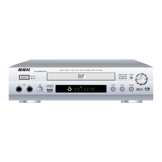
- Page 1 SERVICE MANUAL BBK921D...
-
Page 2: Table Of Contents
CONTENTS SAFETY PRECAUTIONS GENENRAL GUIDELINES PREVENTION OF ELECTRO STATIC DISCHARGE(ESD)TO ELECTROSTATICALLY SENSITIVE(ES) DEVICES PRECAUTION OF LASTER DIODE GENERAL DESCRIPTION PREVENTION OF STATIC ELECTRICITY DISCHARGE GROUNDING FOR ELECTROSTATIC BREAKDOWN PREVENTION 5.1.1 WORKTABLE GROUNDING 5.1.2 HUMAN BODY GROUNDING 5.1.3 HANDING OF OPTICAL PICKUP HANDING PRECAUTIONS FOR TRAVERSE UNIT(OPTICAL PICKUP) ASSENBLING AND DISASSEMBLING THE MECHANISM UNIT DISASSEMBLY PROCEDURE... -
Page 3: Safety Precautions
1.SAFETY PRICAUTIONS 1.1 GENERAL GUIDELINES 1.When servicing,observe the original lead dress.ifa short circuit is found,replace all parts which have been overheated or damaged by the short circuit. 2.After servicing,see to it that all the protective devices such as insulation bamiers,insulation papers shields are properly installed. -
Page 4: Precaution Of Laster Diode
3. Precaution of L aster Diode... -
Page 7: Prevention Of Static Electricity Discharge
5.PREVERTION OF STATIC ELECTRICITY DISCHARGE The laser diode in the traverse unit (optical pickup)may brake down due to static electricity of clothes or human body.Use due caution to electrostatic breakdown when servicing and handling the laser diode. 5.1.Grounding for electrostatic breakdown prevention Some devices such as the DVD player use the optical pickup(laser diode)and the optical pickup will be damaged by static electricity in the working environment.Proceed servicing works under the working environment where grounding works is completed. -
Page 8: Assenbling And Disassembling The Mechanism Unit
6.ASSEMBLING AND DISASSENBLING THE MECHANISM UNIT 6.1Disassembly Procedure 6.2 Terminal P.C.B. 1.Unscrew the screws. 2.Remove the solders. 3.Remove the connectors 5... -
Page 9: Clamp Plate Unit
6.3 Clamp Plate Unit 1.Spread the stopper with hand to silde the tabs and remove the clamp plate unit. 6.4 Tray 1.Lift the tray. 6... -
Page 10: Traverse Block
6.5 Traverse Block 1.Lift the traverse block while spreading the hook of the mechanical chassis chassis unit. 2.Disengage the tabs from the holes of the mechanical chassis unit. 6.6. Traverse Gear 1.Disengage the tabs from the traverse gear 2.Remove the traverse gears B and C. 7... -
Page 11: Optical Pickup Unit
6.7 Optical Pickup Unit 1. Unscrew the screws. 2.Remove the spring holders and the springs. 3.Pull out of the drive shaft and guide shaft. -
Page 12: Precautions In Optical Pickup Replacement
6.7.1. Precautions in optical pickup replacement The optical pickup can be damaged by static electricity from you body.Be sure to take static electricity countermeasures when working around the optical pickup.(Refer to the related page in this Manual about the countermeasures. 1.Do not touch laser diode,actuator and their peripheries. -
Page 13: Disassembling The Middle Chassis
6.8. Disassenbling the Middle Chassis 1.Remove the holders pins. 2.Remove the tab. 3.It lifts while pulling it in the direction of the arrow. 6.9. Disassenbling the Traverse Gear A 1.Remove the traverse gear A. -
Page 14: Disassembling The Spindle Motor Unit
7. Electrical Confirmation 7.1. Video Output (Luminance Signal) Confirmation DO this confirmation after replacing a P.C.B. Measurement point Mode Disc Color bar 75% DVDT-S15 Video output terminal PLAY(Title 46):DVDT-S15 PLAY(Title 12):DVDT-S01 DVDT-S01 Measuring equipment,tools Confirmation value 200mV/dir,10 sec/dir 1000mVp-p±30mV Purpose:To maintain video signal output compatibility. 1.Connect the oscilloscope to the video output terminal and terminate at 75 ohms. -
Page 15: Video Output(Chrominance Signal)Confirmation
7.2. Video Output (Chrominance Signal) Confirmation Do the confirmation after replacing P.C.B. Measurement point Mode Disc Color bar 75% DVDT-S15 Video output terminal PLAY(Title 46):DVDT-S15 PLAY(Title 12):DVDT-S01 DVDT-S01 Measuring equipment,tools Confirmation value Screwdriver,Oscilloscope 200mV/dir,10 sec/dir 621mVp-p±30mV Purpose:To maintain video signal output compatibility. 1.Connect the oscilloscope to the video output terminal and terminate at 75 ohme. -
Page 16: Mpeg Check Waveform
8.MPEG BOARD CHECK WAVEFORM 1. 27MHz WAVEFORM DIAGRAM 2. IC5L0380R PIN.2 WAVEFORM DIAGRAM... -
Page 17: Ic Block Diagram & Description
PRELIMINARY ES6008/18/28/38 DATA SHEET ES60X8 PINOUT DIAGRAM ES60X8 PINOUT DIAGRAM The identical device pinouts for the ES6008, ES6018, ES6028 and ES6038 are shown in Figure 2. HA2/AUX4[4] DSCK AUX[0] AUX[1] DCS0# AUX[2]/IOW# DCS1# AUX[3]/IOR# DB15 AUX[4] DB14 AUX[5] DB13 AUX[6] DB12 AUX[7] LOE#... - Page 18 PRELIMINARY ES6008/18/28/38 DATA SHEET ES60X8 PIN DESCRIPTION ES60X8 PIN DESCRIPTION Table 1 lists the identical pin descriptions for the ES6008, ES6018, ES6028 and ES6038. Table 1 ES60x8 Pin Description Name Number Definition 1,18, 27, 59, 68, I/O power supply. 75, 92, 99, 104, 130, 148, 157, 159, 164, 183, 193, 201...
- Page 19 PRELIMINARY ES6008/18/28/38 DATA SHEET ES60X8 PIN DESCRIPTION Table 1 ES60x8 Pin Description (Continued) Name Number Definition MCLK Audio master clock for audio DAC. TBCK Audio transmit bit clock. SPDIF S/PDIF output. SEL_PLL3 Clock source select. SEL_PLL3 Clock Source Crystal oscillator DCLK input 42, 48 No connect pins.
- Page 20 PRELIMINARY ES6008/18/28/38 DATA SHEET ES60X8 PIN DESCRIPTION Table 1 ES60x8 Pin Description (Continued) Name Number Definition YUV1 YUV1 pixel output data. Internal voltage reference to video DAC. Bypass to ground with 0.1 µF capacitor. VREF YUV2 YUV2 pixel output data. CDAC Video DAC output.
- Page 21 PRELIMINARY ES6008/18/28/38 DATA SHEET ES60X8 PIN DESCRIPTION Table 1 ES60x8 Pin Description (Continued) Name Number Definition HD[11] Host data bus line11. AUX2[3] Aux2 data I/O [3] when selected. IRQ output. HD[12] Host data bus line12. AUX2[4] Aux2 data I/O [4] when selected. C2PO C2PO error correction flag from CD-ROM.
- Page 22 PRELIMINARY ES6008/18/28/38 DATA SHEET LICENSING REQUIREMENTS Table 1 ES60x8 Pin Description (Continued) Name Number Definition AUX[2] Auxiliary port 2. IOW# I/O Write strobe. AUX[3] Auxiliary port 3. IOR# I/O Read strobe. AUX[7:3] 169:166 Auxiliary ports 7:3. LOE# Device output enable. LCS[3:0]# 176:173 Chip select [3:0].
-
Page 23: Functional Description
PRELIMINARY ES6008/18/28/38 DATA SHEET FUNCTIONAL DESCRIPTION FUNCTIONAL DESCRIPTION Figure 3 shows the internal block diagram for the basic Vibratto DVD processor. DSCK_EN DSCK SRAM LA[21:0] DRAM LCS#[3:0] Interface DCS#[1:0] Processor LD[15:0] DRAM Interface DMA[11:0] LWRHL# Interface ESS RISC DWE# LWRLL# DOE# Processor LOE#... - Page 24 IC BLOCK DIAGRAM & DESCRIPTION IC U214 Am29F002B/Am29F002NB 2 Megabit (256 K x 8-Bit) CMOS 5.0 Volt-only Boot Sector Flash Memory DISTINCTIVE CHARACTERISTICS Single power supply operation Embedded Algorithms — 5.0 Volt-only operation for read, erase, and — Embedded Erase algorithm automatically program operations preprograms and erases the entire chip or any combination of designated sectors...
- Page 25 IC BLOCK DIAGRAM & DESCRIPTION PRODUCT SELECTOR GUIDE Family Part Number Am29F002B/Am29F002NB = 5.0 V ± 5% Speed Option = 5.0 V ± 10% -120 Max access time, ns (t Max CE# access time, ns (t Max OE# access time, ns (t Note: See “AC Characteristics”...
- Page 26 IC BLOCK DIAGRAM & DESCRIPTION CONNECTION DIAGRAMS NC on Am29F002NB NC on Am29F002NB RESET# V CC 31 30 PDIP PLCC 17 18 19 20 V SS Standard TSOP RESET# NC on Am29F002NB...
- Page 27 IC BLOCK DIAGRAM & DESCRIPTION PIN CONFIGURATION LOGIC SYMBOL A0–A17 = 18 addresses DQ0–DQ7 = 8 data inputs/outputs A0–A17 = Chip enable DQ0–DQ7 = Output enable = Write enable RESET# = Hardware reset pin, active low (not available on Am29F002NB) = +5.0 V single power supply RESET# (see Product Selector Guide for...
-
Page 28: Ordering Information
IC BLOCK DIAGRAM & DESCRIPTION IC U206 SDRAM-HY57V65162B 4 Banks x 1M x 16Bit Synchronous DRAM DESCRIPTION The Hyundai HY57V651620B is a 67,108,864-bit CMOS Synchronous DRAM, ideally suited for the Mobile applica- tions which require low power consumption and extended temperature range. HY57V651620B is organized as 4banks of 1,048,576x16. - Page 29 IC BLOCK DIAGRAM & DESCRIPTION PIN CONFIGURATION DQ15 DQ14 DQ13 DQ12 DQ11 DQ10 54pin TSOP II 400mil x 875mil 0.8mm pin pitch LDQM UDQM /CAS /RAS A10/AP PIN DESCRIPTION PIN NAME DESCRIPTION The system clock input. All other inputs are registered to the SDRAM on the Clock rising edge of CLK Controls internal clock signal and when deactivated, the SDRAM will be one...
-
Page 30: Functional Block Diagram
IC BLOCK DIAGRAM & DESCRIPTION FUNCTIONAL BLOCK DIAGRAM 1Mbit x 4banks x 16 I/O Synchronous DRAM Self refresh logic Internal Row & timer counter 1Mx16 Bank 3 1Mx16 Bank 2 Row active Decoders 1Mx16 Bank 1 1Mx16 Bank 0 Memory refresh Cell Array... -
Page 31: Absolute Maximum Ratings
IC BLOCK DIAGRAM & DESCRIPTION ABSOLUTE MAXIMUM RATINGS Parameter Symbol Rating Unit °C Ambient Temperature -40 ~ 85 °C Storage Temperature -55 ~ 125 Voltage on Any Pin relative to V -1.0 ~ 4.6 Voltage on V relative to V -1.0 ~ 4.6 Short Circuit Output Current Power Dissipation... - Page 32 IC BLOCK DIAGRAM & DESCRIPTION IC WS7805 POSITIVE-VOLTAGE REGULATORS TO-252 3-Termainal Regulators WS7805DP Output Current Up to 1.5 A No External Components Internal Thermal Overload Protection High Power Dissipation Capability Internal Shot-Circuit Current Limiting (TO-252) Output Transistor Safe-Area Compensation DESCRIPTION This series of fixed-voltage monolithic integrated-circuit voltage regulators designed for a wide range of applications.
-
Page 33: Schematic & Pcb Wiring Diagram
10. SCHEMATIC & P.C.B WIRING DIAGRAM FRONT SCHEMATIC DIAGRAM... - Page 34 FRONT SCHEMATIC DIAGRAM...
- Page 35 POWER BOARD SCHEMATIC DIAGRAM...
- Page 36 POWER BOARD SCHEMATIC DIAGRAM...
- Page 37 OK SCHEMATIC DIAGRAM...
- Page 38 OK SCHEMATIC DIAGRAM...
- Page 39 MIAN SCHEMATIC DIAGRAM...
- Page 40 MIAN SCHEMATIC DIAGRAM...
- Page 41 MIAN SCHEMATIC DIAGRAM...
- Page 42 MIAN SCHEMATIC DIAGRAM...
- Page 43 MIAN SCHEMATIC DIAGRAM...
- Page 44 MIAN SCHEMATIC DIAGRAM...
- Page 45 MIAN SCHEMATIC DIAGRAM...
-
Page 46: Spare Parts List
11. SPARE PARTS LIST BBK921D RU MATERIAL LIST 1 DECODE BOARD MATERIAL SPECIFICATIONS/PART NUMBER QUANTITY LOCATION R213,R335,R287,R2184,L245~L248,R221,L32 CHIP RESISTOR 1/16W 0Ω ±5% 0,R233,R251 CHIP RESISTOR 1/16W 2.2Ω ±5% R250 CHIP RESISTOR 1/16W 10Ω ±5% R214 R382~R399,R2165~R2175,R2177~R2179, CHIP RESISTOR 1/16W 22Ω ±5%... - Page 47 CHIP CAPACITOR 50V 22P ±5% NPO 0603 C201 C299,C314,C2101,C2103,C2105,C2107,C CHIP CAPACITOR 50V 47P ±5% NPO 0603 2109,C291 C260,C262,C263,C265,C266,C268,C269, CHIP CAPACITOR 50V 101 ±5% NPO 0603 C271,C2111,C2114,C2117,C2120,C2123, C2126 CHIP CAPACITOR 50V 331 ±5% NPO 0603 C323,C324 CHIP CAPACITOR 50V 681 ±5% NPO 0603 C316 42.1 CHIP CAPACITOR 50V 681 ±10% 0603 C316...
- Page 48 68.1 IC HCU04 SOP U205 MT48LC4M16A2-75C SOP U204 69.1 IC D4564163G5-A80 SOP U204 69.2 IC HY57V641620HGT-H TSOP U204 CS4360 SSOP U207 AT24C01A SOP U202 GP1F32T JK204 电光转换器 72.1 电光转换器 TX178A JK204 ES6018F QFP U201 MN102H60GHC LQFP U302 MN103S26EGA LQFP U301 BA033FP TO252-3 U305 LM1117MP-1.8 SOT-223...
- Page 49 HIGH VOLTAGE 1/2W680K±5% R501 RESISTOR PORCELAIN 50V 100P ±10% 5mm C505,C507,C509,C511,C513,C514 CAPACITOR PORCELAIN 50V 104 ±20% 5mm C504,C508,C510,C515 CAPACITOR PORCELAIN 1000V 101 +80%-20% 7.5mm C503 CAPACITOR PORCELAIN 14.1 1000V 101 ±10% 7.5mm C503 CAPACITOR PORCELAIN 1000V 103 +80%-20% 7.5mm C502 CAPACITOR CERAMIC CT81 400V 221±20% 10mm...
- Page 50 POWER GRID UT-20 40mH ±20% 10×13 L502 FILTER PHOTOELECTRIC NEC2561 U502 COUPLER PHOTOELECTRIC 38.1 PC817 U502 COUPLER PHOTOELECTRIC 38.2 NEC2501 U502 COUPLER PHOTOELECTRIC 38.3 HS817 U502 COUPLER PHOTOELECTRIC 38.4 817D U502 COUPLER LM7805 GOLD SEALED TO-220 U504 5907KB-2 SOCKET 5 PIN 2.0mm CN501 SOCKET 9 PIN 2.5mm...
- Page 51 CARBON-FILM 1/6W30K±5% SHAPED 7.5 R613,R609,R610 RESISTOR VOLTAGE REGULATOR R0901N-BA1-B10K VR601 POTENTIOMETER PORCELAIN 50V 100P ±10% 5mm C607,C620,C605,C606 CAPACITOR PORCELAIN 50V 561 ±10% 5mm C610,C612 CAPACITOR PORCELAIN 50V 103 ±10% 5mm C603,C604,C616,C619 CAPACITOR PORCELAIN 50V 104 ±20% 5mm C601,C602,C609,C622,C623,C613,C614 CAPACITOR PORCELAIN 50V 392 ±10% 5mm C608,C615 CAPACITOR...
- Page 52 PORCELAIN 50V 103 +80%-20% 2.5mm C401,C405 CAPACITOR PORCELAIN 50V 103 ±20% 2.5mm C401,C405 CAPACITOR CD11C 10V100U±20%5×7 2 C402,C407 DIODE 1N4148 D401 D403 D16312GB QFP U401 11.1 IC PT6312LQ QFP U401 HNV-05SS32 U402 LIGHT TOUCH VERTICAL 6×6×1 K401 K409 RESTORE SWITCH 4921-0 CONNECTION Φ0.6 SHAPED 10mm...
Need help?
Do you have a question about the BBK921D and is the answer not in the manual?
Questions and answers