Table of Contents
Advertisement
Quick Links
SERVICE MANUAL
MICRO COMPONENT SYSTEM
STANDBY/ON
TUNER
TAPE
CD
/RANDOM
/BAND
/REV.MODE
PRE DOWN
PRE UP
REC
REMAIN
REPEAT
/RDS MODE
SLEEP
ST/MONO
INTRO
/RDS SEARCH
TIMER
PROGRAM
DISPLAY
PRE EQ
MODE
/HBS
+
VOLUME
MUTING
BEAT CUT
Ð
RM-SUXM5R REMOTE CONTROL
SP-UXM5
Contents
Safety precautions
Preventing static electricity
Important for laser products
Disassembly method
Adjustment method
Flow of functional operation
until TOC read
M I C R O
C O M P O N E N T
S Y S T E M
STANDBY
/ON
DISPLAY
MODE
TIMER
ON/OFF
SET
RANDOM
BAND
CD
TUNER
PROGRAM
ST/MONO
STOP/CLEAR
SEARCH/TUNING
REPEAT
PHONES
PRESET
REC
DIRECTION
PLAY/PAUSE
A U T O R E V E R S E
FULL LOGIC DECK
CA-UXM55
1-2
1-3
1-4
1-5
1-15
1-18
COPYRIGHT
2002 VICTOR COMPANY OF JAPAN, LTD.
C D - R / R W P L A Y B A C K
U X - M 5 5
OPEN/
CLOSE
REMAIN
/RDS MODE
INTRO/RDS
SEARCH
REV. MODE
TAPE
VOLUME
PRE EQ
/HBS
EJECT
SP-UXM5
Area suffix
E ----------- Continental Europe
EN ------------ Northern Europe
1-19
1-19
1-20
1-21
1-35
No.21190
Jan. 2003
Advertisement
Table of Contents

Related Manuals for JVC UX-M55


Summary of Contents for JVC UX-M55
-
Page 1: Table Of Contents
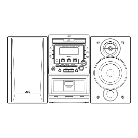
UX-M55 SERVICE MANUAL MICRO COMPONENT SYSTEM UX-M55 Area suffix E ----------- Continental Europe EN ------------ Northern Europe C D - R / R W P L A Y B A C K M I C R O C O M P O N E N T... -
Page 2: Ux-M55
UX-M55 1. This design of this product contains special hardware and many circuits and components specially for safety purposes. For continued protection, no changes should be made to the original design unless authorized in writing by the manufacturer. Replacement parts must be identical to those used in the original circuits. Services should be performed by qualified personnel only. - Page 3 UX-M55 Preventing static electricity 1. Grounding to prevent damage by static electricity Electrostatic discharge (ESD), which occurs when static electricity stored in the body, fabric, etc. is discharged, can destroy the laser diode in the traverse unit (optical pickup). Take care to prevent this when performing repairs.
- Page 4 UX-M55 Important for laser products 5.CAUTION : If safety switches malfunction, the laser is able 1.CLASS 1 LASER PRODUCT to function. 2.DANGER : Invisible laser radiation when open and inter 6.CAUTION : Use of controls, adjustments or performance of lock failed or defeated. Avoid direct exposure to beam.
- Page 5 UX-M55 Disassembly method <Main body section> Replacement of the fuses and power amplifier IC Replacing the fuses (See Fig. 1.) Remove the left side plate according to its disassembly method (see Figs. 6 and 7). Fuses are located inside the left side plate.
- Page 6 UX-M55 Removing the right side plate (See Figs. 4 and 5.) From the right side of the main body, remove the Right side three screws D and three screws E retaining the plate right side plate. (See Fig.4.) Slide the right side plate toward the rear (in the...
- Page 7 UX-M55 Removing the top cabinet (To be loosened) (See Figs. 8 and 9.) Top cabinet Remove the left and right side plates. From the back side of the main body, loosen the two screws F retaining the top cabinet. (See Fig.8.) Rear cabinet Lift the rear part of the top cabinet to remove it.
- Page 8 UX-M55 Removing the CD mechanism CN603 CN601 assembly (See Figs. 13 to 15.) CN701 CN602 Remove the left and right side plates. Remove the top cabinet. Remove the front cabinet assembly. From the top side of the main body, disconnect the wires from the four connectors CN601, CN602, CN603 and CN701 on the CD &...
- Page 9 UX-M55 Removing the main board (See Figs. 18 and 19.) Remove the left and right side plates. Remove the top cabinet. Remove the front cabinet assembly. Remove the CD mechanism assembly. From the inside of the main body, remove the five screws P retaining the bracket.
- Page 10 UX-M55 <Front cabinet assembly section> Remove the left and right side plates. Remove the top cabinet. Front cabinet assembly Key board Remove the front cabinet assembly. Removing the key board (See Fig. 20.) Remove the ten screws V retaining the key board.
- Page 11 UX-M55 Removing the technical door (See Figs. 22 and 23.) Remove the cassette mechanism assembly. Front cabinet assembly Remove the cassette door cover. Technical door Open the technical door, disengage the cassette Cassette torsion spring torsion spring hooked across the front of the front...
-
Page 12: Cd Mechanism Section
UX-M55 <CD mechanism section> Remove the left and right side plates. CD & MCU board Locking board support Remove the top cabinet. CN702 Remove the front cabinet assembly. Remove the CD mechanism assembly. Removing the CD & MCU board (See Figs. 1 and 2.) - Page 13 UX-M55 Removing the tray motor CD mechanism assembly (See Figs. 4 to 7.) Clamper assembly Claw b Remove the CD & MCU board. From the top side of the CD mechanism assembly, open up the claws b and c at the left and right of the clamper assembly and lift the assembly to remove it.
- Page 14 UX-M55 Clamper assembly Front cabinet assembly Replacing the CD pickup unit Claw b (See Figs. 8 to 11.) [Note] Use the following procedure to replace only the CD pickup unit. Remove the left and right side plates. (See Figs. 4 to 7 of "Main body section"...
- Page 15 UX-M55 Adjustment method Measuring instructions required for Measuring instruments adjustment Radio section FM 1kHz, 22.5kHz deviation 1. AM signal generator FM STEREO : 1kHz, 67.5kHz deviation 2. FM signal generator pilot signal 7.5kHz 3. Inter mediate frequency sweep generator AM : 1kHz, 30% modulation 4.
-
Page 16: Tuner Section
UX-M55 Cassette amplifier section Item Measuring condition Check and adjustment procedure Standard value Adjusting part Head azimuth Test tape: Play back the test tape VT702 (8kHz). Output level: Head azimuth adjustment VT702 (8kHz) Adjust the head azimuth adjusting screw so that the... - Page 17 UX-M55 Location of adjusting parts Cassette mechanism section CASSETTE MOTOR Tape Speed Adj. Fig.1 Head output signal Fig.2 Main board (AM VT) T101 L104 R121 (AM IF) (114kHz) IC101 TA2099 L103 L102 (AM RF) (AM OSC) TC101 (AM RF) P201...
-
Page 18: Flow Of Functional Operation Until Toc Read
UX-M55 Flow of functional operation until TOC read Confirm that the voltage at the pin5 of CN703 is Slider turns REST Power ON "H"/"L"/"H" SW ON. Check that the voltage at the pin10(LD) of Laser ON CN704 is +1.35V. Caution... -
Page 19: Maintenance Of Laser Pickup
UX-M55 Maintenance of laser pickup Replacement of laser pickup (1) Cleaning the pick up lens Before you replace the pick up, please try to Turn off the power switch and, disconnect the clean the lens with a alcohol soaked cotton power cord from the AC OUTLET. -
Page 20: Trouble Shooting
UX-M55 Trouble shooting Circuit Symptom Cause Remedy General No sound Speakers are not connected. Check the speaker connection. Wrong function is selected. Set switch to the proper position. Defective volume control Set the volume control to a proper sound level. -
Page 21: Description Of Major Ics
UX-M55 Description of major ICs TC9462F (IC701) : Digital servo single chip processor 1. Terminal layout 2. Pin function Pin No. Symbol Function TEST0 Test mode terminal. Normally, keep at open. Playback speed mode flag output terminal. (Not connect) UHSO... - Page 22 UX-M55 Pin No. Symbol Function TMAXS TMAX detection result output terminal. Selected by command bit (TMPS). TMAX TMAX detection result output terminal. Selected by command bit (TMPS). DIFFERENCE RESULT TMAX OUTPUT Longer than fixed freq. "P2VREF" Shorter than fixed freq.
- Page 23 UX-M55 Pin No. Symbol Function DMOUT This terminal controls IO0 IO3 terminal. At "L" level time, IO0, 1 out feed equalizer signal of 2-state PWM, IO2,3 out disk equalizer signal of 2-state PWM. CKSE Normally, keep at open. DACT DAC test mode terminal. Normally, keep at open.
- Page 24 UX-M55 TMP87EP26F-1J15 (IC601) : MCU 1. Terminal layout (Top view) 2.Pin function Pin No. Symbol Function GND (0V) XOUT Resonator connecting pins for high clock(4-8MHz). For inputting external clock, XIN is used and XOUT is opened. RESET Reset signal input or watchdog timer output/address-trap-reset output XTOUT(P22) Resonator connecting pins for slow clock(32.768kHz)
- Page 25 UX-M55 Pin No. Symbol Function Servo DSP chip enable output BUCK Servo DSP clock output BUS0 Servo DSP command and data I/O BUS1 Servo DSP command and data I/O BUS2 Servo DSP command and data I/O BUS3 Servo DSP command and data I/O TRAY IN(SLOUT) Tray open/close outputs for current sensor drawer type mechanism.
- Page 26 UX-M55 AN7312 (IC202) : Dual recording/Playback pre-amplifier circuit with ALC 1. Terminal layout 2. Block diagram Amp. Ripple Filter Amp. 3. Pin function Pin No. Symbol Function ALC Time Constant ALC time constant by resistance and capacitor ALC Input Ch.1 Right channel ALC input Output Ch.1...
- Page 27 UX-M55 BA4558N (IC401/IC403) : Dual operational amplifier 1. Terminal layout & Block diagram 2. Pin function Pin No. Symbol I/O Function OUT1 A output -IN1 A -input +IN1 A +input +IN2 B +input -IN2 B -input OUT1 -IN1 +IN1 +IN2...
- Page 28 UX-M55 TA2092N (IC703) : Power driver 1. Terminal Layout & Block Diagram 2. Pin function Pin No. Symbol Function PW GND1 PW GND4 PW GND1 Power GND OUT(-)1 OUT(-)4 OUT(-)1 Inverted output for CH1 PW VCC1 PW VCC4 PW VCC1...
- Page 29 UX-M55 TA2099 (IC101) : AM/FM tuner 1. Terminal layout 2. Block diagram DIVIDE DECODE MUTE ANTI BIRDIE LEVEL ST/MO FM/AM BUFF BUFF IF REQ S-METER 3. Pin function Pin No. Symbol Function AM RF IN AM RF input signal terminal...
- Page 30 UX-M55 TA2153FN (IC704) : RF amplifier for digital servo CD system 1. Terminal layout 2. Block diagram RFN2 RFAGC GMAD 30 29 28 27 26 25 24 23 22 21 20 19 18 17 16 AGCIN GVSW RFGO RFRPIN RFCT...
- Page 31 UX-M55 Pin No. Symbol Function RFRP output circuit switching terminal SEL level Bottom detection Peak detection Reference signal (VRO) output terminal RFRP Track count signal output terminal Time constant adjustment terminal for bottom detection RFCT RFRP signal center level output terminal...
-
Page 32: Block Diagram
UX-M55 TC9422F (IC301) : System electronic volume 1.Terminal Layout R-IN1 L-IN1 R-IN2 L-IN2 R-IN3 L-IN3 R-IN4 L-IN4 R SW-OUT L SW-OUT R VR-IN L VR-IN R-B1 L-B1 R-B2 L-B2 R-B3 L-B3 R TONE-OUT L TONE-OUT R-T1 L-T1 Vref DATA 2.Block Diagram... - Page 33 UX-M55 3.Pin Function Pin No. Symbol Function Ground pin L-IN1 Audio signal input pin (L-ch) L-IN2 Audio signal input pin (L-ch) L-IN3 Audio signal input pin (L-ch) L-IN4 Audio signal input pin (L-ch), not connect L SW-OUT Audio signal output pin (L-ch)
- Page 34 UX-M55 TC9257F (IC102) : PLL frequency synthesizer 1. Terminal layout FM VT AM VT DATA MUTE TUNER FM OSC AM OSC ST MONO 2. Block diagram FM L 2 MODULUS 4bit SWALLOW POWER ON FM OSC PRESCALER COUNTER RESET RESET...
-
Page 35: Wiring Connections
UX-M55 Wiring connections P/N: OW23-04910-02 P/N: OW29-21400-01 AM antenna board P/N: OW20-62023-06K FM antenna board P/N: OW20-41063-03 P/N: OW20-41042-35 Earphone board (Forward side) P/N: OW20-42051-36 P/N: OW20-51061-11 P/N: OW20-41062-26 P/N: OW25-61080-01 Tray motor board P/N: OW20-41022-25 P/N: OW20-41032-17 P/N: OW30-00020-06E... -
Page 36: Ux-M55
UX-M55 VICTOR COMPANY OF JAPAN, LIMITED AUDIO & COMMUNICATION BUSINESS DIVISION PERSONAL & MOBILE NETWORK BUSINESS UNIT. 10-1,1Chome,Ohwatari-machi,maebashi-city,371-8543,Japan No.21190 200301...
Need help?
Do you have a question about the UX-M55 and is the answer not in the manual?
Questions and answers