JVC KD-SH9105 Service Manual
Cd receiver
Hide thumbs
Also See for KD-SH9105:
- Instructions manual (69 pages) ,
- Installation & connection manual (4 pages)
Table of Contents
Advertisement
Quick Links
QQ
3 7 63 1515 0
SERVICE MANUAL
6
2003
49834
TE
L 13942296513
1
PRECAUTION. . . . . . . . . . . . . . . . . . . . . . . . . . . . . . . . . . . . . . . . . . . . . . . . . . . . . . . . . . . . . . . . . . . . . . . . . 1-3
2
SPECIFIC SERVICE INSTRUCTIONS . . . . . . . . . . . . . . . . . . . . . . . . . . . . . . . . . . . . . . . . . . . . . . . . . . . . . . 1-5
3
DISASSEMBLY . . . . . . . . . . . . . . . . . . . . . . . . . . . . . . . . . . . . . . . . . . . . . . . . . . . . . . . . . . . . . . . . . . . . . . . 1-6
4
ADJUSTMENT . . . . . . . . . . . . . . . . . . . . . . . . . . . . . . . . . . . . . . . . . . . . . . . . . . . . . . . . . . . . . . . . . . . . . . . 1-27
5
TROUBLE SHOOTING . . . . . . . . . . . . . . . . . . . . . . . . . . . . . . . . . . . . . . . . . . . . . . . . . . . . . . . . . . . . . . . . . 1-32
6
Description of major ICs . . . . . . . . . . . . . . . . . . . . . . . . . . . . . . . . . . . . . . . . . . . . . . . . . . . . . . . . . . . . . . . 1-33
www
.
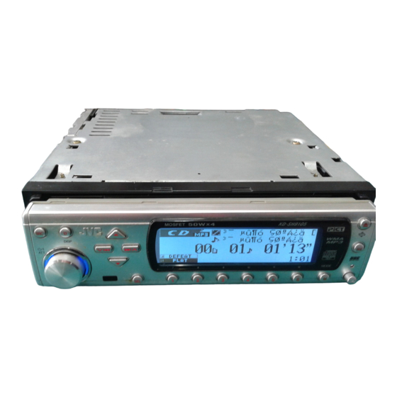
CD RECEIVER
KD-SH9105
ATT
ANGLE
EQ
CD
DAB
DISC
FM
PRESET
PRESET
AM
R D
CH
DISC
AUX
SEL
VOLUME
RM-RK100
TABLE OF CONTENTS
x
ao
u163
y
i
COPYRIGHT © 2003 VICTOR COMPANY OF JAPAN, LIMITED
http://www.xiaoyu163.com
2 9
8
Area Suffix
U -------------------- Other Areas
Q Q
5 0 W x 4
MOSFET
3
6 7
1 3
1 5
D
SRC
DISP
ATT
SEL
1
2
3
co
.
9 4
2 8
KD -SH9105
0 5
8
2 9
9 4
2 8
BBE
MODE
4
5
6
M
m
No.49834
9 9
9 9
2003/6
Advertisement
Table of Contents

Related Manuals for JVC KD-SH9105


Summary of Contents for JVC KD-SH9105
-
Page 1: Table Of Contents
3 7 63 1515 0 SERVICE MANUAL CD RECEIVER 49834 2003 KD-SH9105 Area Suffix U -------------------- Other Areas ANGLE DISC PRESET PRESET 5 0 W x 4 KD -SH9105 MOSFET L 13942296513 DISC DISP VOLUME MODE RM-RK100 TABLE OF CONTENTS PRECAUTION. -
Page 2: Http://Www.xiaoyu163.Com
http://www.xiaoyu163.com 3 7 63 1515 0 SPECIFICATION AUDIO AMPLIFIER SECTION Maximum Power Output Front 50 W per channel Rear 50 W per channel 19 W per channel into 4 Ω, 40 Hz Continuous Power Output (RMS) Front to 20 000 Hz at no more than 0.8% total harmonic distortion. -
Page 3: Precaution
http://www.xiaoyu163.com 3 7 63 1515 0 SECTION 1 PRECAUTION Safety Precautions Burrs formed during molding may be left over on some parts of the chassis. Therefore, pay attention to such burrs in the case of preforming repair of this system. Please use enough caution not to see the beam directly or touch it in case of an adjustment or operation check. - Page 4 http://www.xiaoyu163.com 3 7 63 1515 0 Preventing static electricity Electrostatic discharge (ESD), which occurs when static electricity stored in the body, fabric, etc. is discharged, can destroy the laser diode in the traverse unit (optical pickup). Take care to prevent this when performing repairs. 1.2.1 Grounding to prevent damage by static electricity Static electricity in the work area can destroy the optical pickup (laser diode) in devices such as CD players.
-
Page 5: Specific Service Instructions
http://www.xiaoyu163.com 3 7 63 1515 0 SECTION 2 SPECIFIC SERVICE INSTRUCTIONS This service manual does not describe SPECIFIC SERVICE INSTRUCTIONS. L 13942296513 u163 (No.49834)1-5 http://www.xiaoyu163.com... -
Page 6: Disassembly
http://www.xiaoyu163.com 3 7 63 1515 0 SECTION 3 DISASSEMBLY Main body section Front panel assembly 3.1.1 Removing the front panel assembly (See Fig.1) (1) Push the detach button in the lower right part of the front panel assembly. (2) Remove the front panel assembly in the direction of the arrow. Detach button Fig.1 3.1.2 Removing the top chassis... - Page 7 http://www.xiaoyu163.com 3 7 63 1515 0 3.1.3 Removing the mecha control board (See Fig.7) • Prior to performing the following procedures, remove the top chassis. Mecha control board (1) Disconnect the card wire from the connector CN601 on the mecha control board. (2) Remove the five screws G attaching the mecha control board.
- Page 8 http://www.xiaoyu163.com 3 7 63 1515 0 3.1.5 Removing the motor assembly Motor braket (See Figs.9 to 11) Spring • Prior to performing the following procedures, remove the top chassis. (1) Remove the spring from the motor bracket. (See Fig.9.) (2) Disconnect the wire from the connector CN982 on the main board.
- Page 9 http://www.xiaoyu163.com 3 7 63 1515 0 3.1.6 Removing the main board Arm brackets (L) (See Figs.12 to 16) • Prior to performing the following procedures, remove the top Arm brackets (R) chassis and motor assembly. (1) Disconnect the flexible wires from the connectors CN703 and CN991 on the main board respectively.
- Page 10 http://www.xiaoyu163.com 3 7 63 1515 0 3.1.8 Removing the lifter board Joint d (See Figs.18 to 24) • Prior to performing the following procedures, remove the top chassis and front panel assembly. (1) Disconnect the flexible wire from the connector CN991 on the main board.
- Page 11 http://www.xiaoyu163.com 3 7 63 1515 0 3.1.9 Removing the front board (See Figs.25 to 28) • Prior to performing the following procedures, remove the front Rear panel panel assembly. (1) Remove the six screws X attaching the rear panel to the front panel assembly.
- Page 12 http://www.xiaoyu163.com 3 7 63 1515 0 CD Mechanism section 3.2.1 Removing the top cover (See Figs.1 and 2) (1) Remove the four screws A on the both side of the body. (2) Lift the front side of the top cover and move the top cover backward to release the two joints a.
- Page 13 http://www.xiaoyu163.com 3 7 63 1515 0 3.2.2 Removing the connector board Wires (See Figs.3 to 5) CAUTION: Before disconnecting the flexible wire from the pickup, solder the short-circuit point on the pickup. No observance of this in- struction may cause damage of the pickup. (1) Remove the screw B fixing the connector board.
- Page 14 http://www.xiaoyu163.com 3 7 63 1515 0 3.2.3 Removing the DET switch (See Figs.6 and 7) (1) Extend the two tabs c of the feed sw. holder and pull out the switch. (2) Unsolder the DET switch wire if necessary. switch Connector board Pickup...
- Page 15 http://www.xiaoyu163.com 3 7 63 1515 0 3.2.4 Removing the chassis unit (See Figs.8 and 9) • Prior to performing the following procedure, remove the top Chassis unit cover and connector board. Suspension spring (L) Suspension spring (R) (1) Remove the two suspension springs (L) and (R) attaching the chassis unit to the frame.
- Page 16 http://www.xiaoyu163.com 3 7 63 1515 0 3.2.5 Removing the clamper assembly (See Figs.10 and 11) • Prior to performing the following procedure, remove the top cover. (1) Remove the clamper arm spring. Clamper arm spring (2) Move the clamper assembly in the direction of the arrow to release the two joints d.
- Page 17 http://www.xiaoyu163.com 3 7 63 1515 0 3.2.6 Removing the loading / feed motor assembly (See Figs.12 and 13) • Prior to performing the following procedure, remove the top cover, connector board and chassis unit. (1) Remove the screw C and move the loading / feed motor as- sembly in the direction of the arrow to remove it from the chassis rivet assembly.
- Page 18 http://www.xiaoyu163.com 3 7 63 1515 0 3.2.7 Removing the pickup unit Pickup unit (See Figs.14 to 18) • Prior to performing the following procedure, remove the top cover, connector board and chassis unit. (1) Remove the screw D and pull out the pu. shaft holder from Part e the pu.
- Page 19 http://www.xiaoyu163.com 3 7 63 1515 0 3.2.9 Removing the trigger arm Joint k (See Figs.19 and 20) • Prior to performing the following procedure, remove the top cover, connector board and clamper unit. (1) Turn the trigger arm in the direction of the arrow to release Trigger arm the joint k and pull out upward.
- Page 20 http://www.xiaoyu163.com 3 7 63 1515 0 3.2.11 Removing the mode sw. / select lock arm Link plate Joint t (See Figs.22 and 23) Mode sw. • Prior to performing the following procedure, remove the top plate assembly. Select lock arm (1) Bring up the mode sw.
- Page 21 http://www.xiaoyu163.com 3 7 63 1515 0 3.2.12 Reassembling the mode sw. / select lock arm Select lock arm spring (See Figs.24 to 26) Hook w REFERENCE: Reverse the above removing procedure. Joint v (1) Reattach the select lock arm spring to the top plate and set Joint v the shorter end of the select lock arm spring to the hook w on the top plate.
- Page 22 http://www.xiaoyu163.com 3 7 63 1515 0 3.2.13 Removing the select arm R / link plate Link plate Joint c' Joint r (See Figs.27 and 28) Select arm R Joint b' • Prior to performing the following procedure, remove the top plate assembly.
- Page 23 http://www.xiaoyu163.com 3 7 63 1515 0 3.2.15 Removing the loading roller assembly (See Figs.31 to 33) Loading roller assembly • Prior to performing the following procedure, remove the Roller guide clamper assembly and top plate assembly. spring (1) Push inward the loading roller assembly on the gear side and detach it upward from the slot of the joint g' of the lock arm rivet assembly.
- Page 24 http://www.xiaoyu163.com 3 7 63 1515 0 3.2.16 Removing the loading gear 5, 6 and 7 Loading gear bracket (See Figs.35 and 36) • Prior to performing the following procedure, remove the top Loading gear 6 cover, chassis unit, pickup unit and top plate assembly. (1) Remove the screw K attaching the loading gear bracket.
- Page 25 http://www.xiaoyu163.com 3 7 63 1515 0 3.2.17 Removing the gears Joint p' (See Figs.37 to 40) • Prior to performing the following procedure, remove the top Change plate cover, chassis unit, top plate assembly and pickup unit. rivet assembly • Pull out the loading gear 3. (See Fig.35.) (1) Pull out the feed gear.
- Page 26 http://www.xiaoyu163.com 3 7 63 1515 0 3.2.18 Removing the turn table / spindle motor Turn table (See Figs.41 and 42) • Prior to performing the following procedure, remove the top cover, connector board, chassis unit and clamper assembly. (1) Remove the two screws L attaching the spindle motor as- sembly through the slot of the turn table on top of the body.
-
Page 27: Adjustment
Exclusive dummy load should be used for AM,and FM. For FM (7) Tracking offset meter dummy load,there is a loss of 6dB between SSG output and (8) Test Disc JVC :CTS-1000 antenna input.The loss of 6dB need not be considered since (9) Extension cable for check direct reading of figures are applied in this working standard. - Page 28 http://www.xiaoyu163.com 3 7 63 1515 0 Service mode When entering the service mode, "DATA CLEAR" is displayed without fail. : Initial display : SEEK UP : DISC UP POWER : SEEK DOWN : DISC DOWN SOURCE EPROM all clear & Flash ROM all clear DATA_CLEAR EPROM_CLEAR (Following all contents are cleared.)
- Page 29 http://www.xiaoyu163.com 3 7 63 1515 0 CD_DATA_READ ADJ_NOW ADJ_NOW ADJ_INT FEB__ ____TEB__ OTHERS FGA__ ____TGA__ FEO__ ____RFG__ DISC+/-:FUNCTION TEO__ ADJ_NOW ADJ_INT ADJ_INT FEB__ ____TEB__ OTHERS FGA__ ____TGA__ FEO__ ____RFG__ TEO__ CD data display ADJ_NOW OTHERS Hex. code display ADJ_INT IOP__TEMP____I Total running time display OTHERS IOP__INT__...
- Page 30 http://www.xiaoyu163.com 3 7 63 1515 0 Flow of functional operation unit TOC read Power ON When the laser diode correctly When the pickup correctly moves Set Function CD emits to the inner area of the disc Microprocessor $82 $81 Microprocessor commands Disc inserted commands...
- Page 31 http://www.xiaoyu163.com 3 7 63 1515 0 Maintenance of laser pickup Replacement of laser pickup (1) Cleaning the pick up lens Turn off the power switch and,disconnect the Before you replace the pick up, please try to clean the lens power cord from the ac outlet. with a alcohol soaked cotton swab.
-
Page 32: Trouble Shooting
http://www.xiaoyu163.com 3 7 63 1515 0 SECTION 5 TROUBLE SHOOTING Feed section Is the voltage output at Is the wiring for IC621 Is 3.3V present at IC681 IC621 pin "40" 5V or 0V? pin "40"? pin "6"? Check CD 8V Check the vicinity of and 5V. -
Page 33: Description Of Major Ics
http://www.xiaoyu163.com 3 7 63 1515 0 SECTION 6 Description of major ICs BA3220FV-X (IC171,IC271) : Line out amp • Pin layout 3220 • Block diagram OUTL OUTR RGND LGND L 13942296513 REFR REFL FILTER u163 (No.49834)1-33 http://www.xiaoyu163.com... - Page 34 http://www.xiaoyu163.com 3 7 63 1515 0 AK7740VT (IC101) : Audio DSP with AD/DA converter • Pin layout AINL3 AOUTL2 AINR2 AOUTR2 AINL2 BVSS AINR1 DVSS AINL1 DVDD VREFH INT_RESET 48 pin LQFP AVDD (TOP VIEW) S_RESET AVSS DVSS SCLK DVDD Note) JX , SDIN and SDINA are Pull-down pins •...
- Page 35 http://www.xiaoyu163.com 3 7 63 1515 0 • Pin function Pin No. Symbol Function AINL3 ADC single-ended analog Lch input pin No.3 AINR2 ADC single-ended analog Rch input pin No.2 AINL2 ADC single-ended analog Lch input pin No.2 AINR1 ADC single-ended analog Rch input pin No.1 AINL1 ADC single-ended analog Lch input pin No.1 VREFH...
- Page 36 http://www.xiaoyu163.com 3 7 63 1515 0 BA6956AN (IC981) : Reversible motor driver • Block diagram CONTROL LOGIC • Pin function • Truth table Pin No. Symbol Function OUT1 OUT2 MODE VREF Output high voltage level control terminal Forward rotation mode OUT2 Output terminal for motor Reverse rotation mode...
- Page 37 http://www.xiaoyu163.com 3 7 63 1515 0 HD74HCT126T-X : (IC503) Buffer • Pin arrangement • Pin function Input Output H : High level L : Low level X : Irrelevant Z : Off (Hhigh-impedance)state of a 3-stage output • Block diagram L 13942296513 u163 (No.49834)1-37...
- Page 38 http://www.xiaoyu163.com 3 7 63 1515 0 LH28F160BJHET93 (IC803) : 16M flash memory • Pin layout BYTE# 48-LEAD TSOP STANDARD PINOUT 12mm x 20mm TOP VIEW RY/BY# • Block diagram to DQ Output Input buffer buffer L 13942296513 I/O logic ID code BYTE# register Command...
- Page 39 http://www.xiaoyu163.com 3 7 63 1515 0 • Pin function Pin No. Symbol Function 1 to 8 to A Address input for memory address Address input for memory address Non connection Write enable Reset VCCW Power supply for write/erase Write protect RY/BY# Ready/Busy 16,17...
- Page 40 http://www.xiaoyu163.com 3 7 63 1515 0 IC-PST3424U-X (IC803) : Reset • Pin layout VOUT • Block diagram VOUT Vref • Pin function Pin Name Function L 13942296513 Vout Reset Signal Output PIN VDD PIN / Voltage Detect PIN Non connect VSS PIN u163 1-40 (No.49834)
- Page 41 http://www.xiaoyu163.com 3 7 63 1515 0 NJM2360AM-X (IC921) : DC-DC convertor • Pin layout 1. Cs 2. Es 3. C 4. GND 5. INV 6. Vcc 7. S 8. C • Block diagram Switch Driver collector collector Switch Ipk sense emitter Timing capacitor...
- Page 42 http://www.xiaoyu163.com 3 7 63 1515 0 6.10 NJU7241F33-X (IC504,IC804) : Voltage regulator PIN FUNCTION 1. GND 2. V 3. V 4. +NC 5. STB 6.11 RPM6938-SV4 (IC602) : Remote control receiver • Block diagram Comp Detector conversion trimming circuit magnetic shield 6.12 TDA7404D-X (IC911):Carradio signal processor •...
- Page 43 http://www.xiaoyu163.com 3 7 63 1515 0 6.13 TDA7560-8U (IC301) : Car radio amplifier • Pin layout • Block diagram Vcc1 Vcc2 470uF 100nF ST-BY MUTE HSD/V OUT1+ OUT1- 0.1µF PW-GND OUT2+ L 13942296513 OUT2- 0.1µF PW-GND OUT3+ OUT3- 0.1µF PW-GND OUT4+ OUT4- 0.1µF...
- Page 44 http://www.xiaoyu163.com 3 7 63 1515 0 6.14 UPD784217AGC227 (IC701) : CPU • Pin layout • Block diagram Pin No Symbol Function S.SELECT E-VOL selection output, H: REAR L: FRONT DSP.SELECT DSP or Source direct selection output, H: Source direct L: DSP LINE IN ON OTHER AMP KILL...
- Page 45 http://www.xiaoyu163.com 3 7 63 1515 0 Pin No Symbol Function DETACH Detach detect input; H means detaching DSP data writing ready input INPUT OVER lLINE,AUX input over detecting port, L: Input over S.RESET DSP system reset output INIT.RESET DSP initialize reset output DSP request input, RQ=L: Interface to micom DSP SCK DSP CLOCK OUTPUT...
- Page 46 http://www.xiaoyu163.com 3 7 63 1515 0 L 13942296513 u163 VICTOR COMPANY OF JAPAN, LIMITED AV & MULTIMEDIA COMPANY MOBILE ENTERTAINMENT CATEGORY 10-1,1chome,Ohwatari-machi,Maebashi-city,371-8543,Japan (No.49834) Printed in Japan http://www.xiaoyu163.com...
-
Page 47: Schematic Diagrams
KD-SH9105 3 7 63 1515 0 SCHEMATIC DIAGRAMS CD RECEIVER KD-SH9105 CD-ROM No.SML200306 Area Suffix U -------------------- Other Areas L 13942296513 ANGLE DISC PRESET PRESET 5 0 W x 4 KD -SH9105 MOSFET DISC DISP VOLUME MODE RM-RK100 Contents... -
Page 48: Safety Precaution
KD-SH9105 3 7 63 1515 0 Safety precaution Burrs formed during molding may be left over on some parts of the chassis. Therefore, pay attention to such burrs in the case of preforming repair of this system. Please use enough caution not to see the beam directly or touch it in case of an adjustment or operation check. - Page 49 KD-SH9105 Block diagram 3 7 6 3 1 5 1 5 0 VOUTL VOUTR 1 3 9 4 2 2 9 6 5 1 3 CD mecha board w w w u 1 6 3 Main board Front board...
- Page 50 KD-SH9105 KD-SH9105 Standard schematic diagrams 3 7 6 3 1 5 1 5 0 Main amplifier section IC301 TDA7560 R173 R338 R336 IC171 C333 C336 BA3220FV C180 0.01 C175 100P 100/10 4.7/25 C171 4.7/25 C177 4.7/25 IC151 IC251 C173...
- Page 51 KD-SH9105 LCD & Key control, tuner and DSP section 3 7 6 3 1 5 1 5 0 R852 ACC5V R853 R840 R854 1.5k R841 R855 1.5k R842 1.5k R896 R454 R453 R452 R451 KEY0 D803 C830 1000P S805...
- Page 52 KD-SH9105 KD-SH9105 CD servo control section 3 7 6 3 1 5 1 5 0 RWSEL R585 C585 C587 C589 R613 R581 R583 C611 CD.L-CH 120p 4.7/35 4.7/35 R614 R612 R611 R610 C610 C586 C588 C590 R582 R584 CD.R-CH...
- Page 53 KD-SH9105 3 7 63 1515 0 Printed circuit boards Main board Forward side IC911 CN941 CN322 R913 CN321 R914 R915 R953 R954 C931 C920 C356 R921 CN901 C913 C923 C411 C325 C425 C918 D901 C311 R328 R428 D411 C925...
- Page 54 KD-SH9105 3 7 63 1515 0 Main board Reverse side CN901 C421 C422 C322 C321 CN322 CN941 C324 C323 IC911 R329 CN321 C716 C326 C944 R921 CN702 R371 C931 C913 C356 D901 C923 C920 C362 D702 R370 R368 D353...
- Page 55 KD-SH9105 3 7 63 1515 0 Front board Forward side Reverse side D842 D841 D840 D814 D813 D812 D811 D810 D809 D808 D807 D806 R876 Q802 C830 C829 C823 R848 R847 C828 R845 C824 C825 R844 R843 C826 R839...
- Page 56 KD-SH9105 3 7 63 1515 0 Mecha control board Forward side TH501 R615 R605 R606 R616 C573 R608 C572 R614 R607 C571 R609 R564 R566 R565 C608 R571 R574 R524 C632 C631 R539 R678 R630 R526 R631 R507 R506...
- Page 57 KD-SH9105 3 7 63 1515 0 Mecha control board Reverse side L501 Q683 B681 C674 C652 D681 R514 Q682 R515 L651 L622 C682 L623 R511 L621 Q681 D505 C681 D504 R508 C505 R689 D503 C654 R531 R651 D502 C504...
- Page 58 KD-SH9105 3 7 63 1515 0 L 13942296513 u163 VICTOR COMPANY OF JAPAN, LIMITED AV & MULTIMEDIA COMPANY 10-1,1Chome,Ohwatari-machi,Maebashi-city,371-8543,Japan Printed in Japan (No.49834SCH) 2003/06 http://www.xiaoyu163.com...
-
Page 59: Parts List
KD-SH9105 3 7 63 1515 0 PARTS LIST [ KD-SH9105 ] * All printed circuit boards and its assemblies are not available as service parts. Area suffix U --------------------- Other Areas L 13942296513 - Contents - 3- 2 Exploded view of general assembly and parts list (Block No.M1) 3- 4 CD mechanism assembly and parts list (Block No.MB) - Page 60 KD-SH9105 3 7 63 1515 0 Exploded view of general assembly and parts list Block No. L 13942296513 u163 http://www.xiaoyu163.com...
- Page 61 KD-SH9105 3 7 63 1515 0 General assembly Block No. [M][1][M][M] Symbol No. Part No. Part Name Description Local Symbol No. Part No. Part Name Description Local LV40865-001A MINI SCREW (x3) LV40865-001A MINI SCREW (x2) LV40848-008A SPACER LV40865-001A MINI SCREW...
- Page 62 KD-SH9105 3 7 63 1515 0 CD mechanism assembly and parts list Block No. Grease TN-2001-1013 TNG-87 GP-501MK CFD-005Z GP-501A L 13942296513 u163 http://www.xiaoyu163.com...
- Page 63 KD-SH9105 3 7 63 1515 0 CD mechanism Block No. [M][B][M][M] Symbol No. Part No. Part Name Description Local 30320101T FRAME 30320102T TOP COVER 30320115T DANPER F (x2) 30320116T DANPER R 303205505T CHASSIS RIVET 303205503T CHANGE P. RVT A...
-
Page 64: Electrical Parts List
KD-SH9105 3 7 63 1515 0 Electrical parts list Main board Block No. [0][1][0][0] Symbol No. Part No. Part Name Description Local Symbol No. Part No. Part Name Description Local D381 1SS355-X SI DIODE D382 1SS355-X SI DIODE IC101... - Page 65 KD-SH9105 3 7 63 1515 0 Symbol No. Part No. Part Name Description Local Symbol No. Part No. Part Name Description Local C138 QERF0JM-476Z E CAPACITOR 47uF 6.3V M C335 QERF0JM-476Z E CAPACITOR 47uF 6.3V M C139 QERF1CM-476Z E CAPACITOR...
- Page 66 KD-SH9105 3 7 63 1515 0 Symbol No. Part No. Part Name Description Local Symbol No. Part No. Part Name Description Local C944 NCB31CK-473X C CAPACITOR 0.047uF 16V K R240 NRSA63J-103X MG RESISTOR 10kΩ 1/16W J C961 QERF1HM-105Z E CAPACITOR...
- Page 67 KD-SH9105 3 7 63 1515 0 Symbol No. Part No. Part Name Description Local Symbol No. Part No. Part Name Description Local R441 NRSA63J-0R0X MG RESISTOR 0Ω 1/16W J R786 NRSA63J-103X MG RESISTOR 10kΩ 1/16W J R701 NRSA63J-102X MG RESISTOR 1kΩ...
-
Page 68: Front Board
KD-SH9105 3 7 63 1515 0 Symbol No. Part No. Part Name Description Local Symbol No. Part No. Part Name Description Local BZ961 QAN0023-001Z BUZZER D822 SML-310LT/MN/-X CN321 QGA2501C1-06 CONNECTOR W-B (1-6) D823 SML-310LT/MN/-X CN322 QGA2501C1-07 CONNECTOR W-B (1-7) - Page 69 KD-SH9105 3 7 63 1515 0 Symbol No. Part No. Part Name Description Local Symbol No. Part No. Part Name Description Local R481 NRSA63J-102X MG RESISTOR 1kΩ 1/16W J R863 NRSA63J-331X MG RESISTOR 330Ω 1/16W J R482 NRSA63J-102X MG RESISTOR 1kΩ...
- Page 70 KD-SH9105 3 7 63 1515 0 Symbol No. Part No. Part Name Description Local Symbol No. Part No. Part Name Description Local Q681 2SB1184/QR/-X TRANSISTOR C631 NCS31HJ-471X C CAPACITOR 470pF 50V J C632 NCS31HJ-471X C CAPACITOR 470pF 50V J...
- Page 71 KD-SH9105 3 7 63 1515 0 Symbol No. Part No. Part Name Description Local Symbol No. Part No. Part Name Description Local R535 NRSA63J-101X MG RESISTOR 100Ω 1/16W J R634 NRSA63J-0R0X MG RESISTOR 0Ω 1/16W J R536 NRSA63J-101X MG RESISTOR 100Ω...
- Page 72 KD-SH9105 3 7 63 1515 0 Packing materials and accessories parts list Block No. A8 A9 L 13942296513 KIT: A10A11 A12A13 A14 u163 3-14 http://www.xiaoyu163.com...
- Page 73 KD-SH9105 3 7 63 1515 0 Packing and accessories Block No. [M][3][M][M] Symbol No. Part No. Part Name Description Local LVT1006-001A INST BOOK ENG ARA CHI THA LVT1006-002A INST BOOK LVT1006-003A INST MANUAL ENG ARA KOR CHI THA LVT1006-004A...
Need help?
Do you have a question about the KD-SH9105 and is the answer not in the manual?
Questions and answers