JVC KD-SH9101 Service Manual
Hide thumbs
Also See for KD-SH9101:
- Instructions manual (299 pages) ,
- Service manual (83 pages) ,
- Installation & connection manual (4 pages)
Advertisement
Quick Links
SERVICE MANUAL
11
2003
49841B
KD-SH9101, KD-SH9102,
KD-SH9103, KD-SH9104
1
Precautions . . . . . . . . . . . . . . . . . . . . . . . . . . . . . . . . . . . . . . . . . . . . . . . . . . . . . . . . . . . . . . . . . . . . . . . . . . 1-3
2
SPECIFIC SERVICE INSTRUCTIONS . . . . . . . . . . . . . . . . . . . . . . . . . . . . . . . . . . . . . . . . . . . . . . . . . . . . . . 1-5
3
Disassembly method . . . . . . . . . . . . . . . . . . . . . . . . . . . . . . . . . . . . . . . . . . . . . . . . . . . . . . . . . . . . . . . . . . 1-6
4
Adjustment. . . . . . . . . . . . . . . . . . . . . . . . . . . . . . . . . . . . . . . . . . . . . . . . . . . . . . . . . . . . . . . . . . . . . . . . . . 1-30
5
TROUBLESHOOTING . . . . . . . . . . . . . . . . . . . . . . . . . . . . . . . . . . . . . . . . . . . . . . . . . . . . . . . . . . . . . . . . . 1-33
COPYRIGHT © 2003 VICTOR COMPANY OF JAPAN, LIMITED
CD RECEIVER
ATT
ANGLE
EQ
CD
DAB
DISC
FM
PRESET
PRESET
AM
R D
SRC
D
CH
DISC
DISP
AUX
SEL
ATT
VOLUME
RM-RK100
TABLE OF CONTENTS
KD-SH9101
MOSFET
MODE
1
2
3
4
5
6
M
SEL
Area Suffix
E ------ ContinentalEurope
EX --------- Central Europe
T/P
No.49841B
2003/11
Advertisement

Subscribe to Our Youtube Channel
Related Manuals for JVC KD-SH9101


Summary of Contents for JVC KD-SH9101
-
Page 1: Table Of Contents
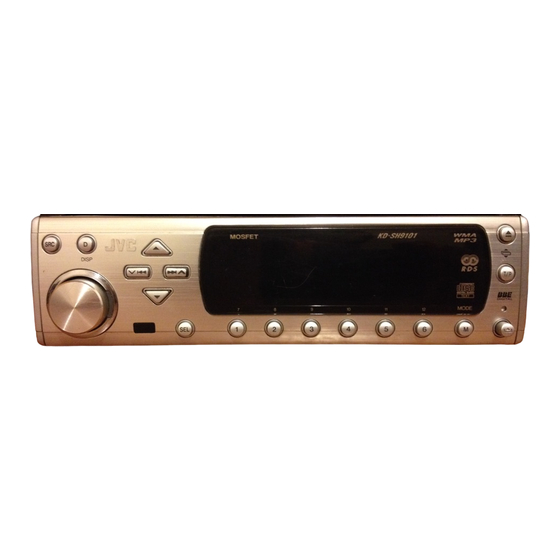
SERVICE MANUAL CD RECEIVER 49841B 2003 KD-SH9101, KD-SH9102, KD-SH9103, KD-SH9104 ANGLE DISC PRESET PRESET KD-SH9101 MOSFET DISC DISP VOLUME MODE RM-RK100 Area Suffix E ------ ContinentalEurope EX --------- Central Europe TABLE OF CONTENTS Precautions ................1-3 SPECIFIC SERVICE INSTRUCTIONS . - Page 2 SPECIFICATION AUDIO AMPLIFIER SECTION Front 50 W per channel Maximum Power Output Rear 50 W per channel 19 W per channel into 4Ω, 40 Hz to 20 000 Hz at no more Front than 0.8% total harmonic distortion. Continuous Power Output (RMS) 19 W per channel into 4Ω, 40 Hz to 20 000 Hz at no more Rear than 0.8% total harmonic distortion.
-
Page 3: Precautions
SECTION 1 Precautions Safety Precautions Burrs formed during molding may be left over on some parts of the chassis. Therefore, pay attention to such burrs in the case of preforming repair of this system. Please use enough caution not to see the beam directly or touch it in case of an adjustment or operation check. - Page 4 Preventing static electricity Electrostatic discharge (ESD), which occurs when static electricity stored in the body, fabric, etc. is discharged, can destroy the laser diode in the traverse unit (optical pickup). Take care to prevent this when performing repairs. 1.2.1 Grounding to prevent damage by static electricity Static electricity in the work area can destroy the optical pickup (laser diode) in devices such as CD players.
-
Page 5: Specific Service Instructions
SECTION 2 SPECIFIC SERVICE INSTRUCTIONS This service manual does not describe SPECIFIC SERVICE INSTRUCTIONS. (No.49841B)1-5... -
Page 6: Disassembly Method
SECTION 3 Disassembly method 3.1 Main body section 3.1.1 Removing the front panel assembly (See Fig.1) (1) Push the detach button in the lower right part of the front panel assembly. Front panel assembly (2) Remove the front panel assembly in the direction of the ar- row. - Page 7 3.1.2 Removing the top chassis (See Figs.2 to 6) • Turn on power. (1) Push the eject button in the upper right part of the front pan- Top chassis el assembly to move the front panel assembly as shown in Fig.2 and turn off power.
- Page 8 3.1.3 Removing the mecha control board (See Fig.7) • Prior to performing the following procedures, remove the top chassis. Mecha control board (1) Disconnect the card wire from the connector CN601 on the mecha control board. (2) Remove the five screws G attaching the mecha control board.
- Page 9 3.1.5 Removing the motor assembly (See Figs.9 to 11) • Prior to performing the following procedures, remove the top chassis. Motor braket Spring (1) Remove the spring from the motor bracket. (See Fig.9.) (2) Disconnect the wire from the connector CN982 on the main board.
- Page 10 3.1.6 Removing the main board (See Figs.12 to 16) • Prior to performing the following procedures, remove the top chassis and motor assembly. (1) Disconnect the flexible wires from the connectors CN703 and CN991 on the main board respectively. (See Fig.12.) (2) Move the front bracket backward until it stops.
- Page 11 3.1.7 Removing the lifter switch board (See Fig.17) • Prior to performing the following procedure, remove the top chassis, motor assembly and main board. Bottom chassis Lifter switch board (1) Remove the two screws T attaching the lifter switch board to the bottom chassis.
- Page 12 3.1.8 Removing the lifter board (See Figs.18 to 24) • Prior to performing the following procedures, remove the top chassis and front panel assembly. • Remove the four screws U attaching the front bracket on the both sides of the main body. (See Figs.19 and 20.) •...
- Page 13 Lifter board Connector cover Fig.23 Fig.24 (No.49841B)1-13...
- Page 14 3.1.9 Removing the front board (See Figs.25 to 28) • Prior to performing the following procedures, remove the front panel assembly. Front panel assembly (1) Remove the six screws X attaching the rear panel to the front panel assembly. (See Fig.25.) (2) Pull out the volume knob from the front side of the front panel assembly.
- Page 15 3.2 CD Mechanism section 3.2.1 Removing the top cover (See Figs.1 and 2) (1) Remove the four screws A on the both side of the body. (2) Lift the front side of the top cover and move the top cover backward to release the two joints a.
- Page 16 3.2.2 Removing the connector board Wires (See Figs.3 to 5) CAUTION: Before disconnecting the flexible wire from the pickup, solder the short-circuit point on the pickup. No observance of this in- struction may cause damage of the pickup. (1) Remove the screw B fixing the connector board. (2) Solder the short-circuit point on the pickup.
- Page 17 3.2.3 Removing the DET switch (See Figs.6 and 7) (1) Extend the two tabs c of the feed sw. holder and pull out the switch. (2) Unsolder the DET switch wire if necessary. switch Connector board Pickup Fig.6 Tab c DET switch DET switch wire Tab c...
- Page 18 3.2.4 Removing the chassis unit (See Figs.8 and 9) • Prior to performing the following procedure, remove the top Chassis unit cover and connector board. Suspension spring (L) Suspension spring (R) (1) Remove the two suspension springs (L) and (R) attaching the chassis unit to the frame.
- Page 19 3.2.5 Removing the clamper assembly (See Figs.10 and 11) • Prior to performing the following procedure, remove the top cover. (1) Remove the clamper arm spring. Clamper arm spring (2) Move the clamper assembly in the direction of the arrow to release the two joints d.
- Page 20 3.2.6 Removing the loading / feed motor assembly (See Figs.12 and 13) • Prior to performing the following procedure, remove the top cover, connector board and chassis unit. (1) Remove the screw C and move the loading / feed motor as- sembly in the direction of the arrow to remove it from the chassis rivet assembly.
- Page 21 3.2.7 Removing the pickup unit Pickup unit (See Figs.14 to 18) • Prior to performing the following procedure, remove the top cover, connector board and chassis unit. (1) Remove the screw D and pull out the pu. shaft holder from Part e the pu.
- Page 22 3.2.9 Removing the trigger arm Joint k (See Figs.19 and 20) • Prior to performing the following procedure, remove the top cover, connector board and clamper unit. (1) Turn the trigger arm in the direction of the arrow to release Trigger arm the joint k and pull out upward.
- Page 23 3.2.11 Removing the mode sw. / select lock arm Link plate Joint t (See Figs.22 and 23) Mode sw. • Prior to performing the following procedure, remove the top plate assembly. Select lock arm (1) Bring up the mode sw. to release from the link plate (joint t) and turn in the direction of the arrow to release the joint u.
- Page 24 3.2.12 Reassembling the mode sw. / select lock arm Select lock arm spring (See Figs.24 to 26) Hook w REFERENCE: Reverse the above removing procedure. Joint v (1) Reattach the select lock arm spring to the top plate and set Joint v the shorter end of the select lock arm spring to the hook w on the top plate.
- Page 25 3.2.13 Removing the select arm R / link plate Link plate Joint r Joint c' (See Figs.27 and 28) Select arm R Joint b' • Prior to performing the following procedure, remove the top plate assembly. (1) Bring up the select arm R to release from the link plate (joint a') and turn as shown in the figure to release the two Joint b' joints b' and joint c'.
- Page 26 3.2.15 Removing the loading roller assembly Loading roller assembly (See Figs.31 to 33) • Prior to performing the following procedure, remove the Roller guide clamper assembly and top plate assembly. spring (1) Push inward the loading roller assembly on the gear side and detach it upward from the slot of the joint g' of the lock arm rivet assembly.
- Page 27 3.2.16 Removing the loading gear 5, 6 and 7 Loading gear bracket (See Figs.35 and 36) • Prior to performing the following procedure, remove the top Loading gear 6 cover, chassis unit, pickup unit and top plate assembly. (1) Remove the screw K attaching the loading gear bracket. The loading gear 6 and 7 come off the loading gear brack- (2) Pull out the loading gear 5.
- Page 28 3.2.17 Removing the gears Joint p' (See Figs.37 to 40) • Prior to performing the following procedure, remove the top Change plate cover, chassis unit, top plate assembly and pickup unit. rivet assembly • Pull out the loading gear 3. (See Fig.35.) (1) Pull out the feed gear.
- Page 29 3.2.18 Removing the turn table / spindle motor Turn table (See Figs.41 and 42.) • Prior to performing the following procedure, remove the top cover, connector board, chassis unit and clamper assembly. (1) Remove the two screws L attaching the spindle motor as- sembly through the slot of the turn table on top of the body.
-
Page 30: Adjustment
(4) Stereo modulator (5) Electric voltmeter Frequency Band (6) Digital tester 87.5MHz to 108.0MHz (7) Tracking offset meter (8) Test Disc JVC :CTS-1000 AM (MW) 522kHz to 1620kHz (9) Extension cable for check AM (LW) 144kHz to 279kHz EXTSH002-22P × 1... - Page 31 When entering the service mode, "DATA CLEAR" is displayed without fail. : Initial display : SEEK UP : DISC UP POWER : SEEK DOWN : DISC DOWN SOURCE EPROM all clear & Flash ROM all clear DATA_CLEAR EPROM_CLEAR (Following all contents are cleared.) NAME_CLEAR ___NOW Execute by "SEL"...
- Page 32 CD_DATA_READ ADJ_NOW ADJ_NOW ADJ_INT FEB__ ____TEB__ OTHERS FGA__ ____TGA__ FEO__ ____RFG__ DISC+/-:FUNCTION TEO__ ADJ_NOW ADJ_INT ADJ_INT FEB__ ____TEB__ OTHERS FGA__ ____TGA__ FEO__ ____RFG__ TEO__ CD data display ADJ_NOW OTHERS Hex. code display ADJ_INT IOP__TEMP____I Total running time display OTHERS IOP__INT__ (Four figures (to 9999), hour only, omit) TEMP__MAX__ P_TOTAL_...
-
Page 33: Troubleshooting
SECTION 5 TROUBLESHOOTING Flow of functional operation untill TOC read (CD) Power ON When the laser diode correctly When the pickup correctly moves Set Function CD emits to the inner area of the disc Microprocessor $82 $81 Microprocessor commands Disc inserted commands 3.3V 3.3V... - Page 34 Feed section Is the voltage output at Is the wiring for IC621 Is 3.3V present at IC681 IC621 pin "40" 5V or 0V? pin "40"? pin "6"? Check CD 8V Check the vicinity of and 5V. IC621. Is 4V present at both Is 6V or 2V present at Check the feed motor sides of the feed motor?
- Page 35 Maintenance of laser pickup Replacement of laser pickup (1) Cleaning the pick up lens Before you replace the pick up, please try to clean the lens Turn off the power switch and,disconnect the power cord from the ac outlet. with a alcohol soaked cotton swab. (2) Life of the laser diode When the life of the laser diode has expired, the following symptoms will appear.
- Page 36 VICTOR COMPANY OF JAPAN, LIMITED AV & MULTIMEDIA COMPANY MOBILE ENTERTAINMENT CATEGORY 10-1,1chome,Ohwatari-machi,Maebashi-city,371-8543,Japan (No.49841B) Printed in Japan...
- Page 37 SCHEMATIC DIAGRAMS CD RECEIVER KD-SH9101,KD-SH9102 KD-SH9103,KD-SH9104 CD-ROM No.SML200311 Area Suffix E ---------- Continental Europe EX -------------- Central Europe ANGLE DISC PRESET PRESET MOSFET KD -SH9101 DISC DISP VOLUME MODE RM-RK100 KD-SH9101 KD-SH9102 KD-SH9103 KD-SH9104 Panel color Alminum Titanium Champagne Gold...
- Page 38 Safety precaution Burrs formed during molding may be left over on some parts of the chassis. Therefore, pay attention to such burrs in the case of preforming repair of this system. Please use enough caution not to see the beam directly or touch it in case of an adjustment or operation check.
- Page 39 CH-L BUSSCK CH-R BUSINT LINE IN PMO+ PANEL CN941 PMO- IC941 SI/SO,SCK SI/SO CD-CH MOTOR JVC BUS IC803 EN801 FLASH ENCODER MEMORY S817 RESET SW S891 to S896 VOL1,VOL2 A1 to A20 PNLSW1 to PNLSW6 D0 to D7 PANEL RESET...
- Page 40 Standard schematic diagrams Main amplifier section IC301 TDA7560 R173 R338 R336 IC171 C333 C336 BA3220FV C180 0.01 C175 100P 100/10 4.7/25 C171 4.7/25 C177 4.7/25 IC151 IC251 C173 R171 C178 4.7/25 TDA7404D TDA7404D 4.7/25 C179 47/16 R172 C176 100/10 C181 0.33 DSPRR C151...
- Page 41 LCD & Key control, tuner and DSP section R852 ACC5V R853 R840 R854 1.5k R841 R855 1.5k R842 1.5k R896 R454 R453 R452 R451 KEY0 D803 C830 1000P S805 S804 S803 S802 S801 Q803 C831 1000P 2SB709A 1SS355 R897 IC805 RPM6938-V4 D804 Q804...
- Page 42 CD servo control section RWSEL R585 C585 C587 C589 R613 R581 R583 C611 CD.L-CH 120p 4.7/35 4.7/35 R614 R612 R611 R610 C610 C586 C588 C590 R582 R584 CD.R-CH X571 120p 4.7/35 4.7/35 Q571 R586 ON5V UN2111 R601 R602 Q572 R603 330k CDON UN2211...
- Page 43 Printed circuit boards Main board Forward side IC911 CN941 CN322 R913 R914 CN321 R915 R953 R954 C931 C920 R921 C356 CN901 C913 C923 C411 C325 C425 C918 D901 C311 R328 R428 D411 C925 C307 D412 D913 C413 D915 C412 C312 C181 C306 C919...
- Page 44 Main board Reverse side CN901 C422 C322 C421 C321 CN322 CN941 C324 C323 IC911 R329 CN321 C716 C326 C944 R921 CN702 R371 C931 C913 C356 D901 C923 C920 C362 D702 R370 R368 D353 C925 R302 C918 R369 C919 D302 VR931 C912 C352 Q322...
- Page 45 Front board Forward side Reverse side D842 D841 D840 D814 D813 D812 D811 D810 D809 D808 D807 D806 R876 Q802 C830 C829 C823 R848 R847 C828 R845 C824 C825 R844 R843 C826 R839 R878 R838 C816 C817 C818 C819 R899 C820 R833 L801...
- Page 46 Mecha control board Forward side TH501 R615 R605 R606 R616 C573 R608 C572 R614 R607 C571 R609 R564 R566 R565 C608 R571 R574 R524 C632 C631 R539 R678 R630 R526 R507 R631 R528 R506 C621 R527 R530 R623 R529 R635 R636 R621 R535...
- Page 47 Mecha control board Reverse side L501 Q683 B681 C674 C652 D681 R514 Q682 R515 L651 L622 C682 L623 R511 L621 D505 Q681 C681 D504 R508 C505 R689 D503 C654 R531 R651 D502 C504 C661 C655 C662 R563 R686 R562 D501 R557 R556 R551...
- Page 48 VICTOR COMPANY OF JAPAN, LIMITED AV & MULTIMEDIA COMPANY MOBILE ENTERTAINMENT CATEGORY 10-1,1chome,Ohwatari-machi,Maebashi-city,371-8543,Japan Printed in Japan (No.49841BSCH)
- Page 49 PARTS LIST [ KD-SH9101 ] [ KD-SH9102 ] [ KD-SH9103 ] [ KD-SH9104 ] * All printed circuit boards and its assemblies are not available as service parts. Area suffix E------------ Continental Europe EX --------------- Central Europe - Contents - 3- 2 Exploded view of general assembly and parts list (Block No.M1)
- Page 50 Exploded view of general assembly and parts list Block No.
- Page 51 General assembly Block No. [M][1][M][M] Symbol No. Part No. Part Name Description Local Symbol No. Part No. Part Name Description Local LV40865-001A MINI SCREW (x3) LV40865-001A MINI SCREW (x2) LV40848-008A SPACER LV40865-001A MINI SCREW (x2) QYSDST2004Z SCREW 2mm x 4mm(x5) LV40865-001A MINI SCREW (x2)
- Page 52 Symbol No. Part No. Part Name Description Local Symbol No. Part No. Part Name Description Local SH910 SH910 4E,SH 4E,SH LV34088-002A PUSH BUTTON 1 LV34095-002A VOL KNOB ASSY 9104E 9104E SH910 LV43183-001A COMP.SPRING 1E,SH SH910 9101E 1E,SH X,SH9 9101E 102E,S X,SH9 LV34089-001A PUSH BUTTON 2...
- Page 53 CD mechanism assembly and parts list Block No. Grease TNG-87 TN-2001-1013 GP-501MK CFD-005Z GP-501A...
- Page 54 CD mechanism Block No. [M][B][M][M] Symbol No. Part No. Part Name Description Local 30320101T FRAME 30320102T TOP COVER 30320115T DANPER F (x2) 30320116T DANPER R 303205505T CHASSIS RIVET 303205503T CHANGE P. RVT A 303205301T CLAMPER ASSY 303205304T SPINDLE MOTOR A 30320502T CLAMPER ARM 30320503T...
- Page 55 Electrical parts list Main board Block No. [0][1][0][0] Symbol No. Part No. Part Name Description Local Symbol No. Part No. Part Name Description Local MA152WK-X SI DIODE D301 1SS355-X SI DIODE IC51 SAA6579T-X D311 RB160M-30-X SB DIODE IC101 AK7740VT D312 RB160M-30-X SB DIODE IC131...
- Page 56 Symbol No. Part No. Part Name Description Local Symbol No. Part No. Part Name Description Local C102 NCB31HK-102X C CAPACITOR 1000pF 50V K C279 QERF1CM-476Z E CAPACITOR 47uF 16V M C103 QERF1HM-225Z E CAPACITOR 2.2uF 50V M C280 NCB31HK-103X C CAPACITOR 0.01uF 50V K C104 QERF1HM-225Z...
- Page 57 Symbol No. Part No. Part Name Description Local Symbol No. Part No. Part Name Description Local C724 NDC31HJ-101X C CAPACITOR 100pF 50V J R122 NRSA63J-472X MG RESISTOR 4.7kΩ 1/16W J C725 NDC31HJ-101X C CAPACITOR 100pF 50V J R123 NRSA63J-473X MG RESISTOR 47kΩ...
- Page 58 Symbol No. Part No. Part Name Description Local Symbol No. Part No. Part Name Description Local R355 NRSA63J-102X MG RESISTOR 1kΩ 1/16W J R741 NRSA63J-472X MG RESISTOR 4.7kΩ 1/16W J R356 NRSA63J-104X MG RESISTOR 100kΩ 1/16W J R742 NRSA63J-472X MG RESISTOR 4.7kΩ...
- Page 59 Front board Symbol No. Part No. Part Name Description Local Block No. [0][3][0][0] R939 NRSA63J-102X MG RESISTOR 1kΩ 1/16W J R941 NRSA63J-104X MG RESISTOR 100kΩ 1/16W J Symbol No. Part No. Part Name Description Local R942 NRSA63J-223X MG RESISTOR 22kΩ 1/16W J R943 NRSA63J-101X MG RESISTOR...
- Page 60 Symbol No. Part No. Part Name Description Local Symbol No. Part No. Part Name Description Local C820 NCB31CK-104X C CAPACITOR 0.1uF 16V K R826 NRSA63J-331X MG RESISTOR 330Ω 1/16W J C821 NCB31HK-223X C CAPACITOR 0.022uF 50V K R827 NRSA63J-331X MG RESISTOR 330Ω...
- Page 61 Symbol No. Part No. Part Name Description Local Symbol No. Part No. Part Name Description Local S810 NSW0066-001X TACT SW C587 NCS31HJ-121X C CAPACITOR 120pF 50V J S811 NSW0066-001X TACT SW C588 NCS31HJ-121X C CAPACITOR 120pF 50V J S812 NSW0066-001X TACT SW C589 NEAD1VM-475X...
- Page 62 Symbol No. Part No. Part Name Description Local Symbol No. Part No. Part Name Description Local C689 NEAD1CM-476X E CAPACITOR 47uF 16V M R586 NRSA63J-303X MG RESISTOR 30kΩ 1/16W J C690 NBE20JM-106X TA E CAPACITOR 10uF 6.3V M R587 NRSA63J-473X MG RESISTOR 47kΩ...
- Page 63 Symbol No. Part No. Part Name Description Local TH501 NAD0022-103X N THERMISTOR 10kΩ 10mW F X501 NAX0385-001X CRYSTAL 24.576MHz X571 NAX0375-001X CRYSTAL 16.9344MHz 3-15...
- Page 64 Packing materials and accessories parts list Block No. A11 A12 KIT: A14A15 A16A17 A18 3-16...
- Page 65 Packing and accessories Block No. [M][3][M][M] Symbol No. Part No. Part Name Description Local Symbol No. Part No. Part Name Description Local LV10840-001A CUSHION LVT1005-001B INST BOOK ENG GER FRE DUT SH910 1E,SH 9102E, LVT1005-002B INST BOOK RUS SPA ITA POL SH910 3E,SH 9104E...
Need help?
Do you have a question about the KD-SH9101 and is the answer not in the manual?
Questions and answers