Table of Contents
Advertisement
Quick Links
Download this manual
See also:
Owner's Manual
Advertisement
Table of Contents

Related Manuals for Standard Horizon HX471S


Summary of Contents for Standard Horizon HX471S
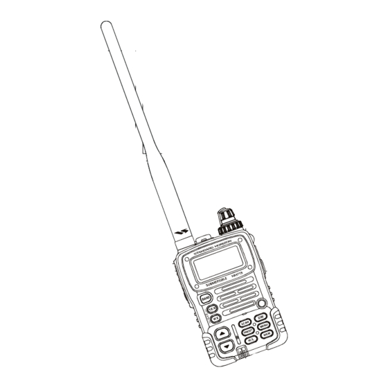
- Page 1 Submersible Multi Band Marine Portable HX471S SERVICE MANUAL EM002N95B...
- Page 2 Introduction This manual provides technical information necessary for servicing the HX471S Transceiver. Servicing this equipment requires expertise in handling surface-mount chip components. Attempts by non-qualified persons to service this equipment may result in permanent damage not covered by the warranty, and may be illegal in some countries.
-
Page 3: Specifications
Specifications GENERAL Frequency Ranges (MHz): 156 MHz - 163.275 MHz (Marine Band + WX Band), Channel Steps: 25 kHz 462.5625 MHz - 467.7125 MHz (FRS Band), Channel Steps: 6.25 kHz 151.82 MHz - 154.60 MHz (MURS), Channel Steps: 5 kHz 88 MHz - 108 MHz (FM Broadcast), Channel Steps: 100 kHz 500 kHz - 1800 kHz (AM Broadcast), Channel Steps: 10 / 9 kHz 108 MHz - 137 MHz (AIR Band), Channel Steps: 25 kHz... -
Page 4: Exploded View & Miscellaneous Parts
Exploded View & Miscellaneous Parts BINDING HEAD SCREW M2X21.7 ( W/ O RING ) U9900145 BINDING HEAD SCREW M2X5 ( W/ O RING ) U9900138 U07225120 PAN HEAD SCREW M2X2.5SUS#1 RA0533700 U9900136 SPECIAL SCREW M2X2.35 PANEL FRAME RA0304300 WASHER U00103002 PAN HEAD SCREW M2X3NI RA0399500 U00104002 PAN HEAD SCREW M2X4NI WINDOW... - Page 5 Block Diagram...
- Page 6 Connection Diagram...
-
Page 7: Circuit Description
(2SC5555). Meanwhile, UHF output from the VCO UNIT is amplified by Q1010 (2SC5374) and applied through di- The HX471S includes three receiver front ends, each opti- ode T/R switch D1021 (DN222) to mixer Q1005 as the first mized for a particular frequency range and mode combi- local signal. -
Page 8: Squelch Control
Circuit Description Demodulated audio is output from pin 9 of the Narrow IF Q3001 and/or Q3003 and/or Q3004 goes on, causing the IC through narrow mute analog switch Q2020 (2SJ364) BUSY/TX lamp D3010 (FRGB1312CE-10-TF) to light. and squelch gate Q2026 (2SJ364) before de-emphasis at Transmitter Signal Flow Q2019 (DTC144EE). -
Page 9: Pll Frequency Synthesizer
Circuit Description UHF Band Transmission (or 1,640) to obtain a reference frequency of 5 kHz (or 6.25 Modulating audio from the CNTL UNIT passes through kHz), which is applied to the phase comparator. Mean- deviation setting D/A converter Q3010 to UHF MOD of while, a sample of the output of VHF VCO Q4004 or UHF the VCO UNIT mounted on the RF UNIT. - Page 10 Circuit Description Note...
-
Page 11: Required Test Equipment
Alignment The HX471S has been carefully aligned at the factory for Required Test Equipment the specified performance across the marine, FRS, MURS, RF Signal Generator with calibrated output level at 500 AIR, AM broadcast and FM broadcast bands. Realignment should therefore not be necessary except in Deviation Meter (linear detector) the event of a component failure. -
Page 12: Alignment Procedure
Alignment Alignment Procedure Receiver Circuit Before alignment, disconnect the antenna from the Set up the test equipment as shown below for receiver transceiver using the Special Screw Driver. alignment. Set up the test equipment as shown for transmitter Maintain the supply voltage at 8.4V DC for all steps. alignment. -
Page 13: Transmitter Circuit
Alignment Sensitivity & Squelch Threshold (FRS Band) Transmitter Circuit Press the [ ] key to select the display to [FRS SQL Set up the test equipment as shown below for trans- ] ([ ] is “00” to “FF” Hex data). The radio now is in mitter alignment. -
Page 14: Transmitter Output (Frs Band)
Alignment to 4.2 kHz (±0.2 kHz), then press the [ MENU ] key to Turn off the Audio generator output. Press the [ ] key to select the display to [FRS 67.0 save the new setting. Press the [ BAND ] key (Change the frequency display ], then press the [ MENU ] key. - Page 15 RF Unit (Lot 1 ~ 3) Circuit Diagram RX: 0 V RX: 8.40 V TX: 2.05 V RX: 0 V RX: 0 V TX: 8.03 V TX: 2.50 V TX: 3.85 V RX: 1.92 V RX: 0 V RX: 1.04 V RX: 0 V RX: 1.87 V TX: 0 V...
- Page 16 RF Unit (Lot 4 ~ 6) Circuit Diagram...
- Page 17 RF Unit (Lot 7 ~) Circuit Diagram...
- Page 18 RF Unit Note...
-
Page 19: Parts Layout (Side A)
RF Unit (Lot 1 ~ 3) Parts Layout (Side A) NJM2904V 2SK3476 2SK3475 2SA1774 (FR) 2SC4154 (LE) 1SS321 (F9) (Q1017) (Q1019) (Q1016) (Q1023, 1025, 1035) (Q1022) (D1027) 2SC5226 (R22) 1SS385 (09) (Q1008) (D1029) 2SC5374 (NA) DAN222 (N) (Q1010) (D1021, 1024, 1025) 2SC5555 (ZD-) (Q1001, 1003, 1005) DTC144EE (26) -
Page 20: Parts Layout (Side B)
RF Unit (Lot 1 ~ 3) Parts Layout (Side B) MB15A01PFV 2SA1774 (FR) 2SC4915 (QY) CPH6102 (AB) DTA144EE (16) 1SS362 (C3) (Q1013) (Q1031) (Q1004, 1007, 1014) (Q1028) (Q1015) (D1002, 1005) 2SC5374 (NA) (Q1011, 1012) 2SC5555 (ZD-) (Q1002, 1006) KRA760U (PK) KRC654U (ND) UMW1 (W1) DAN222 (N) - Page 21 RF Unit (Lot 4 ~ 6) Parts Layout (Side A) NJM2904V 2SK3476 2SK3475 2SA1774 (FR) 2SC4154 (LE) 1SS321 (F9) (Q1017) (Q1019) (Q1016) (Q1023, 1025, 1035) (Q1022) (D1027) 2SC5226 (R22) 1SS385 (09) (Q1008) (D1029) 2SC5374 (NA) DAN222 (N) (Q1010) (D1021, 1024, 1025) 2SC5555 (ZD-) (Q1001, 1003, 1005) DTC144EE (26)
- Page 22 RF Unit (Lot 4 ~ 6) Parts Layout (Side B) MB15A01PFV 2SA1774 (FR) 2SC4915 (QY) CPH6102 (AB) DTA144EE (16) 1SS362 (C3) (Q1013) (Q1031) (Q1004, 1007, 1014) (Q1028) (Q1015) (D1002, 1005) 2SC5374 (NA) (Q1011, 1012) 2SC5555 (ZD-) (Q1002, 1006) KRA760U (PK) KRC654U (ND) UMW1 (W1) DAN222 (N)
- Page 23 RF Unit (Lot 7 ~) Parts Layout (Side A) NJM2904V 2SK3476 2SK3475 2SA1774 (FR) 2SC4154 (LE) 1SS321 (F9) (Q1017) (Q1019) (Q1016) (Q1023, 1025, 1035) (Q1022) (D1027) 2SC5226 (R22) 1SS385 (09) (Q1008) (D1029) 2SC5374 (NA) DAN222 (N) (Q1010) (D1021, 1024, 1025) 2SC5555 (ZD-) (Q1001, 1003, 1005) DTC144EE (26)
- Page 24 RF Unit (Lot 7 ~) Parts Layout (Side B) MB15A01PFV 2SA1774 (FR) 2SC4915 (QY) CPH6102 (AB) DTA144EE (16) 1SS362 (C3) (Q1013) (Q1031) (Q1004, 1007, 1014) (Q1028) (Q1015) (D1002, 1005) 2SC5374 (NA) (Q1011, 1012) 2SC5555 (ZD-) (Q1002, 1006) KRA760U (PK) KRC654U (ND) UMW1 (W1) DAN222 (N) (Q1030)
-
Page 25: Parts List
RF Unit Parts List DESCRIPTION VALUE TOL. MFR'S DESIG VXSTD P/N VERS. LOT SIDE LAY ADR PCB with Components CP7563001 Printed Circuit Board AM002N000 FR009720B FR009720C FR009720D C 1001 CHIP CAP. 39pF UMK105CH390JW-F K22178272 C 1003 CHIP CAP. 68pF UMK105CH680JW-F K22178278 C 1004 CHIP CAP. - Page 26 RF Unit Parts List DESCRIPTION VALUE TOL. MFR'S DESIG VXSTD P/N VERS. LOT SIDE LAY ADR C 1092 CHIP CAP. 0.01uF GRM36B103K16PT K22128804 C 1093 CHIP CAP. 47pF UMK105CH470JW-F K22178274 C 1094 CHIP CAP. 10pF UMK105CH100DW-F K22178258 C 1095 CHIP CAP. 0.001uF UMK105B102KW-F K22178829...
- Page 27 RF Unit Parts List DESCRIPTION VALUE TOL. MFR'S DESIG VXSTD P/N VERS. LOT SIDE LAY ADR C 1177 CHIP CAP. 39pF UMK105CH390JW-F K22178272 C 1178 CHIP CAP. 39pF UMK105CH390JW-F K22178272 C 1180 CHIP CAP. 27pF UMK105CH270JW-F K22178268 C 1181 CHIP CAP. 0.001uF UMK105B102KW-F K22178829...
- Page 28 RF Unit Parts List DESCRIPTION VALUE TOL. MFR'S DESIG VXSTD P/N VERS. LOT SIDE LAY ADR L 1007 M.RFC LK1608 1R0K-T L1690687 L 1008 M.RFC 120uH FLC32T-121J L1690228 L 1009 M.RFC 0.012uH C1608CB-12NG L1691033 L 1010 M.RFC 0.012uH C1608CB-12NG L1691033 L 1011 M.RFC 0.082uH...
- Page 29 RF Unit Parts List DESCRIPTION VALUE TOL. MFR'S DESIG VXSTD P/N VERS. LOT SIDE LAY ADR R 1004 CHIP RES. 1/16W RMC1/16S 221JTH J24189017 R 1005 CHIP RES. 1/16W RMC1/16S 683JTH J24189047 R 1005 CHIP RES. 1/16W RMC1/16S 473JTH J24189045 R 1006 CHIP RES.
- Page 30 RF Unit Parts List DESCRIPTION VALUE TOL. MFR'S DESIG VXSTD P/N VERS. LOT SIDE LAY ADR R 1080 CHIP RES. 3.3k 1/16W RMC1/16S 332JTH J24189031 R 1081 CHIP RES. 3.3k 1/16W RMC1/16S 332JTH J24189031 R 1082 CHIP RES. 4.7k 1/16W RMC1/16S 472JTH J24189033 R 1083...
- Page 31 AF Unit (Lot 1 ~ 2) Circuit Diagram RX: 2.29 V RX: 2.84 V RX: 2.17 V RX: 0 V TX: 0.10 V TX: 0.50 V TX: 0 V TX: 0 V RX: 8.40 V TX: 8.10 V RX: 1.67 V RX: 0.50 V RX: 7.70 V RX: 3.00 V...
- Page 32 AF Unit (Lot 3 ~ 6) Circuit Diagram...
- Page 33 AF Unit (Lot 7 ~) Circuit Diagram...
- Page 34 AF Unit Note...
- Page 35 AF Unit (Lot 1 ~ 2) Parts Layout (Side A) TDA7233D 2SJ364 (4M) 2SA1774 (FR) 2SC4154 (LE) DTA144EE (16) (Q2028) (Q2020, 2026, 2032) (Q2008, 2011, 2014, (Q2003, 2029, 2030, (Q2024) 2015, 2033, 2034) 2036) 2SC4400 (RT4) (Q2010) 2SC4915 (QY) (Q2006) DTC143ZE (E23) DTC144EE (26) DAN222 (N)
- Page 36 AF Unit (Lot 1 ~ 2) Parts Layout (Side B) TA31136 DA221 (K) DAN222 (N) (Q2013) (D2002) (D2003) MC2850 (A7) (D2006, 2007) DTC143ZE (E23) DTC144EE (26) 2SJ364 (4M) 2SC4154 (LE) CPH6102 (AB) (Q2027) (Q2001, 2005, 2019, 2025, (Q2037, 2038) (Q2016, 2017, 2021, 2022) (Q2023) 2039) 2SC4915 (QY)
- Page 37 AF Unit (Lot 3 ~ 6) Parts Layout (Side A) TDA7233D 2SJ364 (4M) 2SA1774 (FR) 2SC4154 (LE) DTA144EE (16) (Q2028) (Q2020, 2026, 2032) (Q2008, 2011, 2014, (Q2003, 2029, 2030, (Q2024) 2015, 2033, 2034) 2036) 2SC4400 (RT4) (Q2010) 2SC4915 (QY) (Q2006) DTC143ZE (E23) DTC144EE (26) DAN222 (N)
- Page 38 AF Unit (Lot 3 ~ 6) Parts Layout (Side B) TA31136 DA221 (K) DAN222 (N) (Q2013) (D2002) (D2003) MC2850 (A7) (D2006, 2007) DTC143ZE (E23) DTC144EE (26) 2SJ364 (4M) 2SC4154 (LE) CPH6102 (AB) (Q2027) (Q2001, 2005, 2019, 2025, (Q2037, 2038) (Q2016, 2017, 2021, 2022) (Q2023) 2039) 2SC4915 (QY)
- Page 39 AF Unit (Lot 7 ~) Parts Layout (Side A) TDA7233D 2SJ364 (4M) 2SA1774 (FR) 2SC4154 (LE) DTA144EE (16) (Q2028) (Q2020, 2026, 2032) (Q2008, 2011, 2014, (Q2003, 2029, 2030, (Q2024) 2015, 2033, 2034) 2036) 2SC4400 (RT4) (Q2010) 2SC4915 (QY) (Q2006) DTC143ZE (E23) DTC144EE (26) DAN222 (N) DAP222 (P)
- Page 40 AF Unit (Lot 7 ~) Parts Layout (Side B) TA31136 DA221 (K) DAN222 (N) (Q2013) (D2002) (D2003) MC2850 (A7) (D2006, 2007) DTC143ZE (E23) DTC144EE (26) 2SJ364 (4M) 2SC4154 (LE) CPH6102 (AB) (Q2027) (Q2001, 2005, 2019, 2025, (Q2037, 2038) (Q2016, 2017, 2021, 2022) (Q2023) 2039) 2SC4915 (QY)
- Page 41 AF Unit Parts List DESCRIPTION VALUE TOL. MFR'S DESIG VXSTD P/N VERS. LOT SIDE LAY ADR PCB with Components CB2313001 Printed Circuit Board AM002N000 FR009710C FR009710D FR009710E C 2001 CHIP CAP. 33pF UMK105CH330JW-F K22178270 C 2002 CHIP CAP. 0.01uF GRM36B103K16PT K22128804 C 2003 CHIP CAP.
- Page 42 AF Unit Parts Layout DESCRIPTION VALUE TOL. MFR'S DESIG VXSTD P/N VERS. LOT SIDE LAY ADR C 2075 CHIP CAP. 0.1uF GRM36B104K10PT K22108802 C 2076 CHIP TA.CAP. 4.7uF 6.3V TEMSVA20J475M-8R K78080031 C 2077 CHIP CAP. 0.01uF GRM36B103K16PT K22128804 C 2078 CHIP CAP.
- Page 43 AF Unit Parts List DESCRIPTION VALUE TOL. MFR'S DESIG VXSTD P/N VERS. LOT SIDE LAY ADR L 2010 M.RFC 10uH KQ1008TE100G L1691216 Q 2001 TRANSISTOR DTC144EE TL G3070075 Q 2002 TRANSISTOR 2SC4915-O(TE85L) G3349158O Q 2003 TRANSISTOR 2SC4154-T11-1E G3341548E Q 2004 TRANSISTOR 2SC4915-O(TE85L) G3349158O...
- Page 44 AF Unit Parts Layout DESCRIPTION VALUE TOL. MFR'S DESIG VXSTD P/N LOT SIDE LAY ADR R 2037 CHIP RES. 1/16W RMC1/16S 103JTH J24189037 R 2038 CHIP RES. 330k 1/16W RMC1/16S 334JTH J24189055 R 2039 CHIP RES. 1/16W RMC1/16S 103JTH J24189037 R 2040 CHIP RES.
-
Page 45: Parts List
AF Unit Parts List DESCRIPTION VALUE TOL. MFR'S DESIG VXSTD P/N VERS. LOT SIDE LAY ADR S 2001 TACT SWITCH SKQTLA N5090110 S 2002 TACT SWITCH SKQTLA N5090110 VR2001 POT. TP76D275N 20F B203.A203 J62800142 XF2001 XTAL FILTER 47.25MHz MF47R2 47.25MHZ H1102347... - Page 46 AF Unit Note...
- Page 47 CNTL Unit (Lot 1 ~ 2) Circuit Diagram RX: 0.47 V TX: 0.84 V RX: 0 V TX: 0.76 V RX: 0 V TX: 0.76 V RX: 3.00 V RX: 8.14 V RX: 2.40 V TX: 3.00 V TX: 7.85 V TX: 2.40 V RX: 0.32 V TX: 0.78 V...
- Page 48 CNTL Unit (Lot 3 ~) Circuit Diagram...
- Page 49 CNTL Unit (Lot 1 ~ 2) Parts Layout (Side A) CPH6202 (CB) (Q3001, 3002, 3003, 3004) SPMA10 (D3001, 3002)
- Page 50 CNTL Unit (Lot 1 ~ 2) Parts Layout (Side B) HD64F2238RTF13 M62364FP NJM3403AV (Q3023) (Q3010) (Q3006) NJM12902V AT24C64 2SJ347 (KS) (Q3009, 3011, 3033) (Q3022) (Q3035) NJM2904V (Q3005) 2SC4154 (LE) (Q3013, 3015,3029, 3032) 2SC4617 (BR) (Q3037) CPH6102 (AB) DTA144EE (16) (Q3026) (Q3008) 2SC5374 (NA) (Q3025)
- Page 51 CNTL Unit (Lot 3 ~) Parts Layout (Side A) CPH6202 (CB) (Q3001, 3002, 3003, 3004) SPMA10 (D3001, 3002)
- Page 52 CNTL Unit (Lot 3 ~) Parts Layout (Side B) HD64F2238RTF13 M62364FP NJM3403AV (Q3023) (Q3010) (Q3006) NJM12902V AT24C64 2SJ347 (KS) (Q3009, 3011, 3033) (Q3022) (Q3035) NJM2904V (Q3005) 2SC4154 (LE) (Q3013, 3015,3029, 3032) 2SC4617 (BR) (Q3037) CPH6102 (AB) DTA144EE (16) (Q3026) (Q3008) 2SC5374 (NA) (Q3025) 2SC5555 (ZD-)
-
Page 53: Cntl Unit
CNTL Unit Parts List DESCRIPTION VALUE TOL. MFR'S DESIG VXSTD P/N VERS. LOT SIDE LAY ADR PCB with Components CB2312001 Printed Circuit Board AM002N000 FR009700D FR009700E C 3002 CHIP CAP. GRM39F105Z10PT K22105001 C 3003 CHIP CAP. 0.001uF UMK105B102KW-F K22178829 C 3005 CHIP TA.CAP. - Page 54 CNTL Unit Parts Layout DESCRIPTION VALUE TOL. MFR'S DESIG VXSTD P/N VERS. LOT SIDE LAY ADR C 3098 CHIP CAP. 0.001uF UMK105B102KW-F K22178829 C 3099 CHIP CAP. 0.047uF GRM36B473K10PT K22108801 C 3100 CHIP CAP. 0.001uF UMK105B102KW-F K22178829 C 3101 CHIP CAP. 0.001uF UMK105B102KW-F K22178829...
- Page 55 CNTL Unit Parts List DESCRIPTION VALUE TOL. MFR'S DESIG VXSTD P/N VERS. LOT SIDE LAY ADR Q 3002 TRANSISTOR CPH6202-TL G3070265 Q 3003 TRANSISTOR CPH6202-TL G3070265 Q 3004 TRANSISTOR CPH6202-TL G3070265 Q 3005 NJM2904V-TE1 G1091677 Q 3006 NJM3403AV(TE1) G1092215 Q 3008 TRANSISTOR DTA144EE TL G3070074...
- Page 56 CNTL Unit Parts Layout DESCRIPTION VALUE TOL. MFR'S DESIG VXSTD P/N VERS. LOT SIDE LAY ADR R 3043 CHIP RES. 330k 1/16W RMC1/16S 334JTH J24189055 R 3044 CHIP RES. 330k 1/16W RMC1/16S 334JTH J24189055 R 3045 CHIP RES. 330k 1/16W RMC1/16S 334JTH J24189055 R 3046...
- Page 57 CNTL Unit Parts List DESCRIPTION VALUE TOL. MFR'S DESIG VXSTD P/N VERS. LOT SIDE LAY ADR R 3128 CHIP RES. 1/16W RMC1/16S 683JTH J24189047 R 3129 CHIP RES. 390k 1/16W RMC1/16S 394JTH J24189056 R 3130 CHIP RES. 390k 1/16W RMC1/16S 394JTH J24189056 R 3131 CHIP RES.
- Page 58 CNTL Unit Note...
-
Page 59: Circuit Diagram
VCO Unit Circuit Diagram Parts Layout Side A Side B DTC143ZE (E23) EC3H03B (C) (Q4003) (Q4002) EC3H07B (G) (Q4004, 4005, 4006) - Page 60 VCO Unit Parts List DESCRIPTION VALUE TOL. MFR'S DESIG VXSTD P/N VERS. LOT SIDE LAY ADR PCB with Components CB2315001 Printed Circuit Board AH009M000 FR007830D C 4001 CHIP CAP. 0.001uF UMK105B102KW-F K22178829 C 4002 CHIP CAP. 0.01uF GRM36B103K16PT K22128804 C 4003 CHIP CAP.
- Page 61 VCO Unit Parts List DESCRIPTION VALUE TOL. MFR'S DESIG VXSTD P/N VERS. LOT SIDE LAY ADR L 4012 M.RFC 0.33uH LK1608 R33K-T L1690412 L 4013 M.RFC 0.033uH HK1608 33NJ-T L1690522 L 4014 M.RFC 0.1uH LK1608 R10K-T L1690407 Q 4002 TRANSISTOR EC3H03B-TL G3070314 Q 4003...
- Page 62 VCO Unit Note...
- Page 63 SW Unit Circuit Diagram Parts Layout Side A SideB Parts List DESCRIPTION VALUE TOL. MFR'S DESIG VXSTD P/N VERS. LOT SIDE LAY ADR PCB with Components CB2374001 Printed Circuit Board AM002N000 FR009780A JP6001 WIRE ASSY GRN 40 2/2 T50504000 JP6002 WIRE ASSY GRN 40 2/2 T50504000...
- Page 64 FVP-31 (Option) Circuit Diagram Parts Layout Side A SideB CMX264 NJM2904V (Q5001) (Q5002)
- Page 65 FVP-31 (Option) Parts List DESCRIPTION VALUE TOL. MFR'S DESIG VXSTD P/N VERS. LOT SIDE LAY ADR Printed Circuit Board AAD17X000 FR0098300 C 5001 CHIP CAP. 0.1uF GRM39B104K16PT K22124805 C 5002 CHIP TA.CAP. 22uF TESVSP0G226M-8R K78060047 C 5003 CHIP CAP. 0.1uF GRM39B104K16PT K22124805 C 5004...
- Page 66 © 2003 VERTEX STANDARD CO., LTD. All rights reserved. Marine Division of VERTEX STANDARD No portion of this manual US Headquarters may be reproduced 10900 Walker Street, Cypress, CA 90630, U.S.A. without the permission of VERTEX STANDARD CO., LTD.
Need help?
Do you have a question about the HX471S and is the answer not in the manual?
Questions and answers