Icom IC-PCR1500 Service Manual
Communications receivers
Hide thumbs
Also See for IC-PCR1500:
- Instruction manual (148 pages) ,
- Service manual (7 pages) ,
- Instruction manual (77 pages)
Table of Contents
Advertisement
Quick Links
GUIDE FOR CD
1) COMPOSION
PCR1500_2500
2) DESCRIPTION
PCR1500_2500.pdf
The service manual for IC-PCR1500 and IC-PCR2500 including all service information in this CD. This file is mainly used
for viewing on the computer display and checking page order to make printed service manual. Or when you want to find a
component, you can find very fast using "FIND" function (except Board Layouts).
PCR1500_2500_A3format.pdf
Consists of A3 format pages (Board layouts, Mechanical parts and disassembly, and etc.). This file is used for
printing out A3 format pages.
PCR1500_2500_A4format.pdf
Consists of A4 format pages (Board layouts, Mechanical parts and disassembly, and etc.). This file is used for
printing out A4 format pages.
PCR1500_2500_MANUAL.pdf
The instruction manual for IC-PCR1500
instruction manual with product and consists of all A4 format pages. If you have A4 format printer, you can print
and make brand new instruction manual any time you want. This file is also very helpful when you want to change
or set product setting condition for adjustment or else.
PCR1500_2500.pdf
FYC
Installer
README.txt
and IC-PCR2500
1
PCR1500_2500_A3format.pdf
PCR1500_2500_A4format.pdf
PCR1500_2500_MANUAL.pdf
ar505eng.exe
. The contents of this file is exactly same as supplied
Advertisement
Table of Contents

Subscribe to Our Youtube Channel
Related Manuals for Icom IC-PCR1500


Summary of Contents for Icom IC-PCR1500
- Page 1 PCR1500_2500.pdf The service manual for IC-PCR1500 and IC-PCR2500 including all service information in this CD. This file is mainly used for viewing on the computer display and checking page order to make printed service manual. Or when you want to find a component, you can find very fast using “FIND”...
- Page 2 ========================================================================================= Icom, Icom Inc. and Icom logo are registered trademarks of Icom Incorporated (Japan) in the United states, the United Kingdom, Germany, France, Spain, Russia and/or other countries. Adobe Acrobat Reader Copyright © 1987-2002 Adobe Systems Incorporated. All rights reserved.
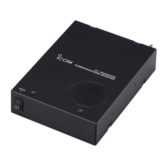
- Page 3 COMMUNICATIONS RECEIVERS iC-pcr1500 iC-pcr2500 S-14222MZ-C1 Jun. 2006...
- Page 4 Addresses are provided on the inside back cover for your before connecting equipment to the receiver. convenience. Icom, Icom Inc. and logo are registered trademarks of Icom Incorporated (Japan) in the United States, the United Kingdom, Germany, France, Spain, Russia and/or other countries.
-
Page 5: Table Of Contents
TABLE OF CONTENTS SECTION SPECIFICATIONS SECTION INSIDE VIEWS SECTION DISASSEMBLY INSTRUCTIONS SECTION CIRCUIT DESCRIPITON RECEIVER CIRCUITS............4-1 PLL CIRCUITS . - Page 6 ¤ ¤ ¤ ¤ SECTION 1 SPECIFICATIONS ¤ ¤ ¤ ¤ ¤ ¤ ¤ ¤ ¤ ¤ M GENERAL ¤ ¤ • Frequency coverage – – – – – – – – – – – – – – – – –...
- Page 7 ¤ ¤ M RECEIVER • Receive system : Triple-conversion superheterodyne and down converter • Intermediate frequencies : 1st: 266.700 MHz, 2nd: 10.700 MHz, 3rd: 450 kHz (except for WFM mode) • Sensitivity • ; . v – µ – µ –...
- Page 8 SECTION 2 INSIDE VIEWS LOGIC UNIT L5V regulator (IC9: AN78L05) USB +3.3V regulator IC1: S-812C33 CPU5V regulator Q31: 2SB789 (IC3: XC6202P502PR) USB HUB TOP VIEW Q32: 2SC4116 (IC32: USB2502) VCC line controller Q4: 2SJ377 Q6: DTC144EU AF amplifier (IC12: LA4425A) AF +8V regulator (Q5: 2SB1201, Q8: XP1501) +33V regulator...
- Page 9 • MAIN-A UNIT RF circuits TOP VIEW Down converter circuits 1st VCO circuits 2nd VCO circuits Buffer (Q60: 2SC4617) DDS REF 8V regulator (Q90: XP4311) Noise blanker amplifier (Q68: 2SK882) DDS circuits APCO5V regulator (Q77: 2SA1832) D3.3V regulator (Q10: UNR9111) ATT circuits BOTTOM VIEW DVCO +5V regulator...
- Page 10 • MAIN-B UNIT (IC-PCR2500 only) TOP VIEW BOTTOM VIEW HF filter circuits ATT circuits 1st mixer (IC14: SPM5001) 1st VCO circuits +5V regulator (Q23: UNR9111) 1st IF amplifier (Q44: 3SK131) PLL 3.3V regulator (IC9: S-812C33AMC) 2st VCO circuits 2nd mixer (IC19: TA4107F) Buffer RSSI meter amplifier...
- Page 11 SECTION 3 DISASSEMBLY INSTRUCTIONS • Removing the top cover and shield covers r Remove the shield covers D and E* in the direction of q Unscrew 8 screws, A. the arrow. w Unplug the connectors B and C from the LOGIC unit. e Remove the top cover in the direction of the arrow.
-
Page 12: Circuit Descripiton
SECTION 4 CIRCUIT DESCRIPTION The 50–1300 MHz signals from the antenna are passed 4-1 RECEIVE CIRCUITS through the anttenuator (D1, D3), band switch (D7) and LPF 4-1-1RF CIRCUITS (MAIN-A/-B UNITS) (L5, C33, C34), then applied to one of the RF circuit. The MAIN-A UNIT has eight RF circuits and one down converter circuit to provide wide receiving range. - Page 13 • 1300–3300 MHz* In FM or AM mode, the 2nd IF signal is passed through the The 1300–3300 MHz signals from the antenna are applied to FI5 (band width=50 kHz) via mode switches (D66, D70), the down converter circuit where those signals are converted into the lower frequencies.
- Page 14 <3rd IF AND DEMODULATOR CIRCUITS (FM)> D73 FI9 3rd IF signal to the AM demodulator circuits D95 FI8 10.25 MHz 3rd IF amp. TCXO 3rd LO signal D72 FI7 amp. amp. Noise Noise Amp. Detector D/A converter Limit’r Quodrature Amp. RSSI Detector IF IC (IC24)
-
Page 15: Pll Circuits
pulse-type signal at the noise detector section, and output • 1st VCO’s from pin 13 as the “NOIS” signal. The “NOIS” signal is The 1st VCO is composed by two VCO’s; as the 1st LO applied to the CPU (IC18, pin 16). And the CPU outputs signal generator for 0.01–483.29 MHz and 483.3–3300 MHz control signals “LSTB,”... -
Page 16: Digital Mode Operation With Ut-122
The phase difference is output from pin 5 as a pulse type The phase difference is output from pin 5 as a pulse type signal after being passed through the internal charge pump. signal after being passed through the internal charge pump. The output signal is applied to the VCO (Q19, D43) after The output signal is applied to the VCO (Q27, Q28, D52, being converted into the DC voltage (lock voltage) at the... -
Page 17: Power Supply Circuits
4-4 POWER SUPPLY CIRCUITS VOLTAGE LINE DESTINATION VOLTAGE LINE DESTINATION Same voltage as the connected power supply. AP5V Optional UT-122. AF+8V AF power amplifi er (IC12). OP5V Optional UT-108/UT-118. Electric volume (IC17), tone fi lter (IC21), AF switch A+5V (IC4, IC23), etc. MAIN-A UNIT. -
Page 18: Cpu Port Allocation
4-5 CPU PORT ALLOCATION PORT DESCRIPTION NAME 4-5-1 CPU (LOGIC UNIT; IC18) Input port for mute signal from the attached PORT DESCRIPTION RXMUTE optional unit via the pin 24 of J2018. NAME “High”=While the audio output is muted. Outputs strobe signal to the expander (MAIN-B BMST2 Outputs control signal to the AF switch (IC4, UNIT;... -
Page 19: Adjustment Procedures
SECTION 5 ADJUSTMENT PROCEDURES 5-1 PREPARATION When adjusting IC-PCR1500/PCR2500, controller for the R1500/R2500 and JIG cable (see the illust below) are required. ¤ REQUIRED TEST EQUIPMENTS EQUIPMENT GRADE AND RANGE EQUIPMENT GRADE AND RANGE Frequency range : 0.1–3300 MHz Standard signal Output level : 0.1 µV to 32 mV... - Page 20 <FOR IC-PCR1500 ADJUSTMENT> • CONTROLLER ¤ ENTERING ADJUSTMENT MODE q Set the direction of the [VOL] to 12 o'clock (11–1 o'clock). [VOL] w Push and hold [TS•MODE]+[ATT•PRIO]+[NB•AGC] [SET•LOCK] [TS•MODE] +[MONI•T/T-SCAN] key, and turn the power switch (MAIN UNIT) ON. ¤ KEY ASSIGNMENTS FOR THE ADJUSTMENT MODE •...
-
Page 21: Main-A Unit Adjustment
5-2 MAIN-A UNIT ADJUSTMENT ADJUSTMENT OPERATION VALUE REFERENCE 1 • Connect a frequency counter to the J5 connector on the MAIN-A 10.25000 MHz FREQUENCY UNIT (see the illust below). [REF] 2 • Push [TS•MODE]/[SET•SKIP] to store the set value. 1 • Preset the adjustment items as below before the “BPF“ adjustment. Automatic adjustment [LT1]–[HTF] [AGA]... - Page 22 5-2 MAIN-A UNIT ADJUSTMENT (coninued) ADJUSTMENT OPERATION VALUE S-METER 1 • Set the SSG as; Automatic adjustment [NS0]–[WS6] Frequency : Specifi ed frequency* Modulation : None † Level : Specifi ed level 2 • Push [TS•MODE]/[SET•SKIP] to store the adjustment value. –...
-
Page 23: Main-B Unit Adjustment (Pcr2500 Only)
5-3 MAIN-B UNIT ADJUSTMENT (PCR2500 only) ADJUSTMENT OPERATION VALUE 1 • Set the adjustment items as below before the “BPF” adjustment. Automatic adjustment [LT1]–[HTF] [AGA] : “8A” [IFA] : “25” 2 • Connect an SSG to the antenna connector “ANT1” and set as; Frequency : Specifi... - Page 24 5-3 MAIN-B UNIT ADJUSTMENT (PCR2500 only; continued) ADJUSTMENT OPERATION VALUE S-METER 1 • Set the SSG as; Automatic adjustment [NS0]–[WS6] Frequency : Specifi ed frequency* Modulation : None † Level : Specifi ed level 2 • Push [SET•SKIP] to store the adjustment value. –...
- Page 25 • ADJUSTMENT ITEM LIST ADJUSTMENT ADJUSTMENT ADJUSTMENT ADJUSTMENT † † † † Disp. Level Disp. Level Disp. Level Disp. Level ITEM ITEM ITEM ITEM (dBµ/dBm) (dBµ/dBm) (dBµ/dBm) (dBµ/dBm) REFERENCE 11/–96 LA2* 34/–73 25/–82 REF* – FREQUENCY 18/–89 LA3* 34/–73 35/–72 35/–72 26/–81 LA4*...
-
Page 26: Logic Unit
SECTION 6 PARTS LIST [LOGIC UNIT] • IC-PCR1500 IC-PCR2500 [LOGIC UNIT] ORDER DESCRIPTION LOCATION ORDER DESCRIPTION 1790001250 S.DIO MA2S111-(TX) 79.2/41.3 LOCATION 1790001250 S.DIO MA2S111-(TX) 1180002391 S.REG S-812C33AMC-C2N-G 47.3/40.1 [EUR-1], [FRA-1] only T 84.2/38.7 1110002350 S.IC BA6161F 10.3/20.8 1790001250 S.DIO MA2S111-(TX) 83/38.7... - Page 27 [LOGIC UNIT] [LOGIC UNIT] ORDER ORDER DESCRIPTION DESCRIPTION LOCATION LOCATION 7030005080 S.RES ERJ2GEJ 823 X (82 k) 92.6/21.3 R248 7030005290 S.RES ERJ2GEJ 682 X (6.8 k) 82.7/33.6 7030005240 S.RES ERJ2GEJ 473 X (47 k) 127/28.5 R249 7030005290 S.RES ERJ2GEJ 682 X (6.8 k) 83.3/32 7030005060 S.RES ERJ2GEJ 333 X (33 k) 69.6/16.9...
- Page 28 [LOGIC UNIT] [LOGIC UNIT] ORDER ORDER DESCRIPTION DESCRIPTION LOCATION LOCATION 4030006900 S.CER C1608 JB 1H 103K-T 7.4/16.8 C142 4030016790 S.CER ECJ0EB1C103K 72.9/14.4 4030016790 S.CER ECJ0EB1C103K 42.8/48.3 C144 4030017780 S.CER ECJ0EB1E472K 78.8/16.5 4030006900 S.CER C1608 JB 1H 103K-T 131.2/38.2 C148 4510008490 S.ELE EEE1CS100SR 86.5/17.3 4030006900 S.CER C1608 JB 1H 103K-T 106.4/29...
-
Page 29: Main-A Unit
[LOGIC UNIT] [LOGIC UNIT] ORDER ORDER DESCRIPTION DESCRIPTION LOCATION LOCATION C2116* 4030017730 S.CER ECJ0EB1E471K 25.5/20.9 6910014690 S.BEA MPZ1608S221A-T 117.6/56.8 C2117* 4030017430 S.CER ECJ0EC1H101J 34.6/20.4 6910012350 S.BEA MMZ1608Y 102BT 43.3/50.3 C2122* 4030016780 S.CER ECJ0EB1C153K 24.1/19.3 EP10 6910014690 S.BEA MPZ1608S221A-T 20.9/57.5 C2123* 4030017460 S.CER ECJ0EB1E102K 36/20.4 EP15 6910012350 S.BEA MMZ1608Y 102BT... - Page 30 [MAIN-A UNIT] [MAIN-A UNIT] ORDER ORDER DESCRIPTION DESCRIPTION LOCATION LOCATION 1590001810 S.TR XP1113 (TX) 15.6/50.6 1790001621 S.DIO 1SV308 (TPL3 F) 13.5/53.9 1590003380 S.TR UNR9111J-(TX) 17.2/46.4 1720000650 S.VCP 1SV286 (TPH3) 14.3/34.5 1530003260 S.TR 2SC5006-T1 6.6/55 1790001621 S.DIO 1SV308 (TPL3 F) 8.1/9.1 1530003450 S.TR 2SC4835-R (TX) 14.9/20.9...
- Page 31 [MAIN-A UNIT] [MAIN-A UNIT] ORDER ORDER DESCRIPTION DESCRIPTION LOCATION LOCATION 2020001751 CER SFVLF10M7MF00-B0 6140004591 S.COL LR-517A 30.4/8.6 2020001451 CER SFTLF10M7GA00-B0 6200002631 S.COL NLV25T-R10J 50.3/9 2020001470 CER CFWLA450KL6A002-B0 6200001981 S.COL NLV25T-1R0J 43.3/43 2020001460 CER CFWLA450KHFA-B0 6200003950 S.COL HF50ACC 322513-T 69.6/22.2 2020001210 CER CFWLA450KEFA-B0 6200001981 S.COL NLV25T-1R0J 43.8/47.6...
- Page 32 [MAIN-A UNIT] [MAIN-A UNIT] ORDER ORDER DESCRIPTION DESCRIPTION LOCATION LOCATION 7030005040 S.RES ERJ2GEJ 472 X (4.7 k) 11.9/57.6 R119 7030008290 S.RES ERJ2GEJ 183 X (18 k) 40.8/10.8 7030005240 S.RES ERJ2GEJ 473 X (47 k) 13.5/22.3 R120 7030010040 S.RES ERJ2GEJ-JPW 36.9/9.1 7030005040 S.RES ERJ2GEJ 472 X (4.7 k) 13.4/49.5 R121...
- Page 33 [MAIN-A UNIT] [MAIN-A UNIT] ORDER ORDER DESCRIPTION DESCRIPTION LOCATION LOCATION R229 7030005040 S.RES ERJ2GEJ 472 X (4.7 k) 65.7/10.1 R340 7030004980 S.RES ERJ2GEJ 101 X (100) 80.2/65.3 R230 7030005000 S.RES ERJ2GEJ 471 X (470) R341 7030004980 S.RES ERJ2GEJ 101 X (100) 77.4/60 [FRA-1], [SEA-1], [EXP-2] B 43.7/28.6...
- Page 34 [MAIN-A UNIT] [MAIN-A UNIT] ORDER ORDER DESCRIPTION DESCRIPTION LOCATION LOCATION R444 7030005050 S.RES ERJ2GEJ 103 X (10 k) 76/22 R550 7030005220 S.RES ERJ2GEJ 223 X (22 k) 111.2/45.9 R445 7030005240 S.RES ERJ2GEJ 473 X (47 k) 77.6/21.9 R551 7030005100 S.RES ERJ2GEJ 154 X (150 k) 112.9/43.6 R446 7030007290 S.RES ERJ2GEJ 222 X (2.2 k)
- Page 35 [MAIN-A UNIT] [MAIN-A UNIT] ORDER ORDER DESCRIPTION DESCRIPTION LOCATION LOCATION 4030017400 S.CER ECJ0EC1H220J 10.1/24.6 C168 4030017730 S.CER ECJ0EB1E471K 24/37.3 4030017430 S.CER ECJ0EC1H101J 5.9/12.5 C169 4030017730 S.CER ECJ0EB1E471K 23.5/34.3 4030017730 S.CER ECJ0EB1E471K 17.6/52.9 C170 4030017420 S.CER ECJ0EC1H470J 14.8/44.2 4030017350 S.CER ECJ0EC1H020B 11/53.6 C171 4030017460 S.CER ECJ0EB1E102K...
- Page 36 [MAIN-A UNIT] [MAIN-A UNIT] ORDER ORDER DESCRIPTION DESCRIPTION LOCATION LOCATION C266 4030016930 S.CER ECJ0EB1A104K 39/43.7 C371 4030017460 S.CER ECJ0EB1E102K 60.3/60.2 C267 4030016790 S.CER ECJ0EB1C103K 38.4/45 C372 4030017780 S.CER ECJ0EB1E472K 115.5/61.6 C268 4030016930 S.CER ECJ0EB1A104K 56.2/13.4 C373 4030017460 S.CER ECJ0EB1E102K 66.9/42.3 C269 4030017460 S.CER ECJ0EB1E102K 39/42.8...
- Page 37 [MAIN-A UNIT] [MAIN-A UNIT] ORDER ORDER DESCRIPTION DESCRIPTION LOCATION LOCATION C474 4030016930 S.CER ECJ0EB1A104K 115/19.7 C572 4030016930 S.CER ECJ0EB1A104K 74.6/28.3 C475 4030016930 S.CER ECJ0EB1A104K 115/12.1 C573 4030017460 S.CER ECJ0EB1E102K 79.1/34.5 C476 4030016930 S.CER ECJ0EB1A104K 114.9/5 C574 4030016930 S.CER ECJ0EB1A104K 121.4/55.5 C477 4030017720 S.CER ECJ0EB1H331K 115.5/14.2...
- Page 38 [MAIN-A UNIT] [MAIN-B UNIT] (IC-PCR2500 only) ORDER ORDER DESCRIPTION DESCRIPTION LOCATION LOCATION C694 4030017460 S.CER ECJ0EB1E102K 65.5/53.9 1590001960 S.TR XP4311 (TX) 97.8/36.5 C695 4030017460 S.CER ECJ0EB1E102K 40.2/44.8 1590002010 S.TR XP1114 (TX) 120/21.9 C696 4030017460 S.CER ECJ0EB1E102K 40.2/43 1590002010 S.TR XP1114 (TX) 117.5/21.9 C697 4030017460 S.CER ECJ0EB1E102K...
- Page 39 [MAIN-B UNIT] (IC-PCR2500 only) [MAIN-B UNIT] (IC-PCR2500 only) ORDER ORDER DESCRIPTION DESCRIPTION LOCATION LOCATION D103 1790001240 S.DIO MA2S728-(TX) 87.2/28.8 L119 6200001981 S.COL NLV25T-1R0J 45/22.9 D110 1750000940 S.DIO ISS400 TE61 85.4/10.2 L120 6200010540 S.COL C2012C-47NG-A 40.8/53 L122 6200007001 S.COL ELJRE 82NGFA 67.4/33 L123 6200010210 S.COL C2012C-22NG-A...
- Page 40 [MAIN-B UNIT] (IC-PCR2500 only) [MAIN-B UNIT] (IC-PCR2500 only) ORDER ORDER DESCRIPTION DESCRIPTION LOCATION LOCATION R113 7030005080 S.RES ERJ2GEJ 823 X (82 k) 41/11 R228 7030004980 S.RES ERJ2GEJ 101 X (100) 75/35.6 R114 7030004980 S.RES ERJ2GEJ 101 X (100) 33.4/5.7 R229 7030005040 S.RES ERJ2GEJ 472 X (4.7 k) 64.7/6.3 R115...
- Page 41 [MAIN-B UNIT] (IC-PCR2500 only) [MAIN-B UNIT] (IC-PCR2500 only) ORDER ORDER DESCRIPTION DESCRIPTION LOCATION LOCATION R362 7030005040 S.RES ERJ2GEJ 472 X (4.7 k) 113.9/14.3 R504 7030005160 S.RES ERJ2GEJ 105 X (1 M) 108.1/31.6 R363 7030005030 S.RES ERJ2GEJ 152 X (1.5 k) 105.8/7.4 R505 7030005170 S.RES ERJ2GEJ 474 X (470 k)
- Page 42 [MAIN-B UNIT] (IC-PCR2500 only) [MAIN-B UNIT] (IC-PCR2500 only) ORDER ORDER DESCRIPTION DESCRIPTION LOCATION LOCATION C107 4030017430 S.CER ECJ0EC1H101J 20.1/4.2 C270 4030017460 S.CER ECJ0EB1E102K 46.7/17.1 C108 4030017460 S.CER ECJ0EB1E102K 21.4/11.9 C271 4030016790 S.CER ECJ0EB1C103K 32/32.9 C113 4030017460 S.CER ECJ0EB1E102K 22.1/4 C273 4030017460 S.CER ECJ0EB1E102K 47.1/35.8 C114...
- Page 43 [MAIN-B UNIT] (IC-PCR2500 only) [MAIN-B UNIT] (IC-PCR2500 only) ORDER ORDER DESCRIPTION DESCRIPTION LOCATION LOCATION C375 4030017460 S.CER ECJ0EB1E102K 54.9/42.2 C548 4030016790 S.CER ECJ0EB1C103K 92.1/50.1 C379 4510008540 S.ELE EEE1CA100SR 110.1/49.7 C549 4030016790 S.CER ECJ0EB1C103K 113.4/21.2 C380 4510008660 S.ELE EEE0JA220SR 99.2/46.4 C550 4030016790 S.CER ECJ0EB1C103K 93/48.5 C382...
-
Page 44: Main Unit
[MAIN UNIT] [MAIN-B UNIT] (IC-PCR2500 only) ORDER ORDER DESCRIPTION DESCRIPTION LOCATION LOCATION 7030005120 S.RES ERJ2GEJ 102 X (1 k) 3.9/4.3 C725 4030017440 S.CER ECJ0EC1H221J 34.5/9.7 7030005120 S.RES ERJ2GEJ 102 X (1 k) 3.6/2.8 C726 4030017440 S.CER ECJ0EC1H221J 34.5/8.7 7030005120 S.RES ERJ2GEJ 102 X (1 k) 14.2/5.1 C727... - Page 45 [MAIN UNIT] ORDER DESCRIPTION LOCATION 4030016930 S.CER ECJ0EB1A104K 19.6/18.6 4030016790 S.CER ECJ0EB1C103K 12.4/14.6 4030017420 S.CER ECJ0EC1H470J 3.1/7.2 4030017420 S.CER ECJ0EC1H470J 4.3/7.5 4030017420 S.CER ECJ0EC1H470J 3/11.3 4030017760 S.CER ECJ0EB1H222K 19.6/20.4 4030017420 S.CER ECJ0EC1H470J 7.8/9.9 4030017420 S.CER ECJ0EC1H470J 12.9/9.3 4030017420 S.CER ECJ0EC1H470J 3.2/8.8 4030017460 S.CER ECJ0EB1E102K...
- Page 46 SECTION 7 MECHANICAL PARTS AND DISASSEMBLY [CHASSIS PARTS] [MAIN-B UNIT] (IC-PCR2500 only) REF. NO. ORDER NO. DESCRIPTION QTY. REF. NO. ORDER NO. DESCRIPTION QTY. 6510015550 Connector BNC-R117 6510018450 Connector TMP-S01X-B1 6510015550 Connector BNC-R117 [PCR2500 only] 6510018450 Connector TMP-S01X-B1 2260002400 Switch DS850K-S-LG 8510014460 2509 VCO cover 8510014460...
- Page 47 Unit: mm (inch) DIGITAL UNIT MP23(C) MP23(C) MP1(D) MP6(C) MP5(C)* MP9(C) MP23(C) W5(C) W1(C) S1(C) MP3(C) MP22(C) MP3(L) J2(C)* MP2(L) 1.5( 41(1 MP30(C) W12(C)* 42.5(1 MP23(C) MP32(C) MP4(L) MP11(C)* 146(5 W13(C) SP1(C) LOGIC UNIT W14(C) W8(L) W8(C) MP21(C)* MP22(C) W7(C) MP1(L) MP21(C)* MP8(MB)*...
- Page 48 SECTION SECTION 8 SEMICONDUCTOR INFORMATION PARTS LIST • TRANSISTORS AND FET'S • DIODES NAME SYMBOL INSIDE VIEW NAME SYMBOL INSIDE VIEW NAME SYMBOL INSIDE VIEW NAME SYMBOL INSIDE VIEW 1SR154-400 1SS400 1SV284 2SA1832 GR 2SK880 Y XP4311 1SV286 1SV308 MA2S077 MA2S111 MA2S728 2SB1123 T-TD...
- Page 49 SECTION 9 BOARD LAYOUTS The combination of this page and the next page shows the unit layout in the same configuration as the actual P.C. Board. Power switch Internal speaker • LOGIC UNIT (TOP VIEW) (J4:CHASSIS) (CHASSIS: SP1) J2022 J2021 to MAIN-A unit “J2”...
- Page 50 • LOGIC UNIT (BOTTOM VIEW) 9 - 2...
- Page 51 The combination of this page and the next page shows the unit layout in the same configuration as the actual P.C. Board. • MAIN-A UNIT (TOP VIEW) WFDT SCAD SMAD NOIS FDET to LOGIC unit “J24” IFOUT MST2 DPSTB MST0 P1STB P2STB MST1...
- Page 52 • MAIN-A UNIT (BOTTOM VIEW) 9 - 4...
- Page 53 • MAIN-B UNIT (TOP VIEW; PCR2500 only) To antenna connector (CHASSIS: J2) BWFDT BSMAD BAFO BNOIS to LOGIC unit BFDET “J2022” BIFOUT B+5V B+5V B+8V BMST3 BPPS BMST1 BP1STB BP2STB BMST2 to LOGIC unit “J2021” BDAT BDSTB B+33V B–5V to MAIN-A unit “J5”...
- Page 54 • MAIN-B UNIT (BOTTOM VIEW; PCR2500 only) 9 - 6...
-
Page 55: Top View
The combination of this page and the next page shows the unit layout in the same configuration as the actual P.C. Board. • UT-122 (Optinal product: DIGTAL UNIT for [IC-PCR2500: USA-3]) (TOP VIEW) CIRQ D IF FLASH RXD AFOUT CPU RES FLASH TXD RMUT TEMP... - Page 56 • UT-122 (Optinal product: DIGTAL UNIT for [IC-PCR2500: USA-3]) (BOTTOM VIEW) 9 - 8...
- Page 57 SECTION 10 BLOCK DIAGRAM IC3: XC6202P502 DC-JACK CPU5V CPU5V APPWR CPU5V IC2: BA6161F POWER-SW D2: 1SS355 Q9: 2SC4617 CR-816 (12 MHz) D26: HVC376 RESET +33V AP5V RIPPLE AP5V +33V RESET EXPAND CLOCK Q2019: 2SB798 IC35: S-80942 SHIFT CTRL Q2021: 2SC4116 Q5: 2SB1201 D2012: MA2S111 IC34, IC36: CD4094...
- Page 58 Q1: UNR9213 BAND1 Q2: UNR9113 BAND1 Q8: 2SC4617 0.01–1.799999 MHz BAND BAND 1st-Mix ATTC CTRL 2nd-IF: 10.7 MHz 2nd-Mix A+8V A+8V D29: 1SV308 A+5V A+5V FI1: EFCH266MWNT1 D56: 1SV307F Q66: 3SK131 D66: MA2S077 D98: DA221 D70: MA2S077 IC14: IFCON IC19: TA4107F 1.8–14.999999 MHz HF8V BAND2...
-
Page 59: Main-B Unit (Pcr2500 Only)
Q12: 2SC4835 BVCO1 CTRL 2nd-IF: 10.7 MHz 1st-Mix 50–149.999999 MHz BBAND5 BBAND5 Q66: BTUENV2, 3 2nd-Mix BTUENV1 BBAND5 BRFAGC D66: MA2S077 FI1: EFCH266MWNT1 3SK131 D70: MA2S077 BIFCON IC19: TA4107F 2ND IF MODE MODE 2ND IF 1st IF BAND BAND GAIN CTRL MODE Q15:... - Page 60 SECTION 11 VOLTAGE DIAGRAM R22 330 HEC2711-01-620 MPZ1608S221A 2.21V 5.0V R197 C233 CPU5V R199 11.83V MPZ1608S221A XC6202P502PR IC35 100K HVC376B S-80942CNMC CR-816 5.10V 12.00MHz AN78L05M R171 B4B-ZR-SM4-TF PWRSW IC34 2SJ377 R173 CD4094BPWR LSTB 1 STR BUSY VDAT 4.98V FDETSEL 3 CLK APPWR 4 Q1 FDETINH...
- Page 61 EP2001 C2201 MPZ1608S221A NFM18PC104R1C3 –5V J2021 52808-1871 C2202 NFM21CC223R1H3 +33V EP2002 C2200 MPZ1608S221A BDSTB R2147 C2198 BMDAT BFDET PCR2500 only R2148 C2197 R2126 BMCK MAIN-B UNIT C2194 R2127 C2164 C2167 BMST2 3.9K 0.022 0.01 BFDET R2226 C2195 BCMAD BP2STB R2105 INPUT 100K C2193...
- Page 62 0.01 MHz–1.8 MHz 0.01 MHz–1300 MHz 266.7MHz (1.5 MHz) C134 C173 1SV308 5.6H 0.0015 5.6H 1SV307 4.3V 3.6V C2012C C2012C EFCH266MWNT1 C218 TMP-S01X-B1 D1 1SV308 0.001 1SV308 C148 R536 D102 DA221 270P 1SV307 R615 R143 C576 1.8 MHz–15MHz C150 C163 C619 C178 100H...
- Page 63 C670 MAIN-A UNIT C671 0.001 2.72V C313 L135 6.13V 2.56V Measurement conditions L123 L126 0.01 6.0V C371 18nH C2012C Explanatory notes C2012C 0.001 2SC4617 0.89V for voltage value 3SK131 L169 R476 LS-513 MA2S077 R339 SFVLF10M7MF00 C505 L168 +B LINE IC19 TA4107F 0.25V MA2S077...
- Page 64 266.7MHz (1.5 MHz) 4.38V EFCH266MWNT1 R590 C154 C199 3SK318 C2012C C2012C 0.0047 1SV308 50 MHz–150 MHz 470µ 50 MHz–1.3 GHz C107 1SV308 TMP-S01X-B1 0.001 D1 1SV308 0.001 1SV308 100P C2012C C2012C 100P 100P 0.50V C315 180K 0.001 1.0H 4.74V 4.32V 1st mixer MP13 UNR9113J...
- Page 65 C670 6.13V 4.39V C671 S-812C33AMC 0.001 C313 2nd mixer 0.01 R145 R131 R339 SFVLF10M7MF00 C505 L168 L135 MA2S077 MA2S077 0.01 L123 L126 C371 18nH C2012C C2012C 0.001 R461 R535 R132 3SK131 R146 L169 R476 BDAT1 LS-513 MA2S077 IC19 TA4107F 2SC4617 3.32V 5.97V 10.7 MHz (26 kHz)
- Page 66 3.3V IC14 S-80928CNMC- 470p 0.001 G8Y G 5.0V 3.3V CPU_RES IC17 1 OUT XC6204B332M 2 VDD HN58X2416TI 3.3V DVDD 3.3V 3 VSS VOUT 0.01 8 VCC CVDD 1.5V 0.001 470p 0.001 0.001 0.001 0.001 1.5V XC9215A15CMR NLFV25T-330K-PF 1.5V CE/MODE VOUT 0.001 3.3V XC6204B332M...
- Page 68 S-14222MZ-C1 1-1-32, Kamiminami, Hirano-ku, Osaka 547-0003, Japan © 2006 Icom Inc.
Need help?
Do you have a question about the IC-PCR1500 and is the answer not in the manual?
Questions and answers