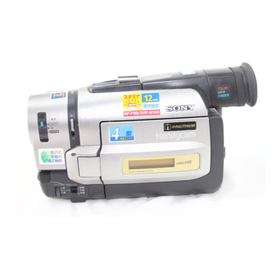
Sony Handycam Vision CCD-TRV89E Service Manual
Hi8 video camera recorder
Hide thumbs
Also See for Handycam Vision CCD-TRV89E:
- Operating instructions manual (132 pages) ,
- Service manual (24 pages)
Table of Contents
Advertisement
SERVICE MANUAL
B MECHANISM
Video camera recorder
System
Video recording system
CCD-TRV95/TRV95PK/TRV99 :
4 rotary heads (SP/LP independent heads)
CCD-TRV89E/TRV95E/TRV99E :
2 Rotary heads
Helical scanning FM system
Audio recording system
Rotary heads, FM system
Video signal
CCD-TRV95 (US, CND)/TRV99 :
NTSC color, CCIR standards
CCD-TRV95 (E, JE)/TRV95PK :
NTSC color, EIA standards
CCD-TRV89E/TRV95E/TRV99E :
PAL color CCIR standards
Usable cassette
8mm video format cassette
Hi8 or standard 8
Recording / Playback time
CCD-TRV95/TRV95PK/TRV99 :
(using 120 min. cassette)
SP mode: 2 hours
LP mode: 4 hours
CCD-TRV89E/TRV95E/TRV99E :
(using 90 min. cassette)
SP mode: 1 hours and 30 minutes
LP mode: 3 hours
Fastforward/rewind time
CCD-TRV95/TRV95PK/TRV99 :
(using 120 min. cassette) Approx. 5 min.
CCD-TRV89E/TRV95E/TRV99E :
(using 90 min. cassette) Approx. 5 min.
MICROFILM
CCD-TRV89E/TRV95/TRV95E/TRV95PK/
Photo : CCD-TRV99E
: RMT-717
SPECIFICATIONS
Image device
CCD (Charge Coupled Device)
Viewfinder
Electronic viewfinder
CCD-TRV89E : Monochrome
CCD-TRV95/TRV95E/TRV95PK/
TRV99/TRV99E :
Color 113,578 (521 x 218)
Lens
Combined power zoom lens
Filter diameter 17/16 in. (37 mm)
CCD-TRV95 (US,CND)/TRV95E/
TRV99 :
18 x (Optical), 72 x (Digital)
CCD-TRV89E/TRV95 (E, JE)/
TRV95PK/TRV99E :
18 x (Optical), 220 x (Digital)
Focal distance
3/16 - 8 in. (4.1 - 73.8 mm)
When converted to a 35 mm still
camera
1 7/8 - 33 1/2 in. (47.2 - 850 mm)
Color temperature
Auto
Minimum illumination
0.7 lux (F 1.4)
0 lux (in NightShot mode)*
* Object invisible for the dark can be
shot with infrared lighting.
Illumination range
0.7 lux to 100,000 lux
Recommended illumination
More than 100 lux
TRV99/TRV99E
CCD-TRV89E/TRV95/TRV95PK/TRV99E
Hong Kong Model
For MECHANISM ADJUSTMENTS, refer to
the "8mm Video MECHANICAL ADJUSTMENT
MANUAL VII" (9-973-801-11).
LCD screen
Picture
4 inches measured diagonally
3 1/4 x 2 3/8 in.(80.7 x 58.9 mm)
On-screen display
TN LCD/TFT active matrix method
Total dot number
112.086 (479 x 234)
Input and output connectors
S video input/output
(CCD-TRV89E/TRV95/TRV95PK/
TRV99/TRV99E only)
4-pin mini DIN
Luminance signal :
1 Vp-p, 75 ohms, unbalanced
Chrominance signal
CCD-TRV95/TRV95PK/TRV99 :
0.286 Vp-p, 75 ohms, unbalanced
CCD-TRV89E/TRV95E/TRV99E :
0.3 Vp-p, 75 ohms, unbalanced
Video input/output
(CCD-TRV89E/TRV95/TRV95PK/
TRV99/TRV99E only)
Phono jack, 1 Vp-p, 75 ohms, unbalanced
HVIDEO CAMERA RECORDER
RMT-708/717
US Model
Canadian Model
CCD-TRV95/TRV99
E Model
AEP Model
UK Model
CCD-TRV95E
CCD-TRV89E/TRV99E
Tourist Model
CCD-TRV89E/TRV95/TRV99E
Australian Model
Chinese Model
CCD-TRV89E/TRV99E
Audio input/output
(CCD-TRV89E/TRV95/TRV95PK/
TRV99/TRV99E only)
Phono jacks (2: stereo L and R) 327
mV, (at output impedance 47 kilohms)
impedance less than 2.2 kilohms
RFU DC OUT
Special minijack, DC 5V
Headphone jack
Stereo minijack (ø 3.5 mm)
LANC control jack
Stereo mini-minijack (ø 2.5 mm)
MIC jack
Mini jack, 0.388mV low impedance
with 2.5 to 3.0 V DC, output impedance
6.8 kilohms (ø 3.5 mm) Stereo type
Speaker
Dynamic speaker
Intelligent accessory shoe
8-pin connector
General
Power requirements
7.2 V (battery pack)
8.4 V (AC power adaptor)
— Continued on next page —
Advertisement
Table of Contents

Related Manuals for Sony Handycam Vision CCD-TRV89E


Summary of Contents for Sony Handycam Vision CCD-TRV89E
- Page 1 CCD-TRV95/TRV95PK/TRV99 : Electronic viewfinder Phono jacks (2: stereo L and R) 327 4 rotary heads (SP/LP independent heads) On-screen display CCD-TRV89E : Monochrome mV, (at output impedance 47 kilohms) TN LCD/TFT active matrix method CCD-TRV89E/TRV95E/TRV99E : CCD-TRV95/TRV95E/TRV95PK/ impedance less than 2.2 kilohms...
-
Page 2: Camera Recording
CRITIQUES POUR LA SÉCURITÉ DE FONCTIONNEMENT. NE COMPONENTS WITH SONY PARTS WHOSE PART NUMBERS REMPLACER CES COMPOSANTS QUE PAR DES PIÈCES SONY APPEAR AS SHOWN IN THIS MANUAL OR IN SUPPLEMENTS DONT LES NUMÉROS SONT DONNÉS DANS CE MANUEL OU PUBLISHED BY SONY. - Page 3 – 3 –...
- Page 4 VMC-91 : CCD-TRV95E RMT-708 : Except CCD-TRV95E/TRV99/TRV99E !º 2 pin conversion adaptor (1) 2 AC-L10A/L10B/L10C AC power adaptor CCD-TRV89E : E, HK/TRV95 : E/TRV95PK/TRV99E : E, HK, AUS 3 NP-F330 Battery pack (1) !¡ 2 pin conversion adaptor (1) 4 CR2025 Lithium Battery (1) CCD-TRV89E : JE/TRV95 : JE/TRV99E : JE The lithium battery is already installed in your camcorder.
-
Page 5: Service Note
SERVICE NOTE 1. POWER SUPPLY DURING REPAIRS In this unit, about 10 seconds after power is supplied (8.4V) to the battery terminal using the service power cord (J-6082-223-A), the power is shut off so that the unit cannot operate. Battery switch This following two methods are available to prevent this. -
Page 6: Self-Diagnosis Function
SELF-DIAGNOSIS FUNCTION 1. Self-diagnosis Function 2. Self-diagnosis display When problems occur while the unit is operating, the self-diagnosis When problems occur while the unit is operating, the counter of the function starts working, and displays on the viewfinder or Display viewfinder or Display window shows a 4-digit display consisting window what to do. -
Page 7: Self-Diagnosis Code Table
4. Self-diagnosis Code Table Self-diagnosis Code Symptom/State Correction Block Detailed Function Code Remove the cassette, and insert it again after one hour. Condensation. Clean with the optional cleaning cassette. Video head is dirty. Non-standard battery is used. Use the InfoLITHIUM battery. LOAD direction. -
Page 8: Table Of Contents
TABLE OF CONTENTS SERVICE NOTE 2. DISASSEMBLY Power Supply During Repairs ......... 5 2-1. Removal of Front Panel Block ......... 2-1 To Take out a Cassette when not Eject (Force Eject) ..5 2-2. Removal of Cabinet (S) Block ......... 2-1 2-3. - Page 9 Backlight Comsumption Current Adjustment (VF-122 board) ............5-24 White Balance Adjustment (VF-123 board) ... 5-24 1-5. Monochrome Electronic Viewfinder System Adjustments (CCD-TRV89E) .............. 5-25 1-5-1. Horizontal Slant Check ........... 5-25 1-5-2. Centering Adjustment ..........5-25 1-5-3. Focus Adjustment ............ 5-25 1-5-4.
- Page 10 5-2. MECHANICAL SECTION ADJUSTMENT ....5-33 6. REPAIR PARTS LIST 2-1. Operating without a Cassette .......... 5-33 2-2. Tape path Adjustment .............5-33 6-1. Exploded Views ............6-1 Preparations for adjustments ........5-33 6-1-1. Cabinet (L) Block Assembly ........6-1 6-1-2. Front Panel Block Assembly ........6-2 5-3.
-
Page 38: Disassembly
CCD-TRV89E/TRV95/TRV95E/TRV95PK/TRV99/TRV99E SECTION 2 DISASSEMBLY The eqipment can be removed using the following procedure. VIDEO CAMERA RECORDER 2-8. EVF BLOCK-2 2-9. EVF BLOCK-2 2-1. FRONT PANEL BLOCK 2-11. CASSETTE LID ASSEMBLY (B/W) (COLOR) 2-2. CABINET (S) 2-3. CABINET (R) BLOCK 2-4. EVF BLOCK-1 2-5. -
Page 39: Removal Of Cabinet (R) Block
2-3. REMOVAL OF CABINET (R) BLOCK 2-5. REMOVAL OF EVF BLOCK-1 (B/W) 2 Flexible flat cable(FCC-235) 5 Tapping screw CN008,4P 4 Tapping screw 7 Two tapping screws 3 Tapping screw 6 VF base assembly 6 Connector CN933,11P 2 Two screws (M2x4) 8 Three tapping 3 Three screws (M2x4) -
Page 40: Removal Of Cf-52 Board And Control Switch Block (Mf-8500)
2-7. REMOVAL OF CF-52BOARD AND CONTOROL 2-8. REMOVAL OF EVF BLOCK-2 (B/W) SWITCH BLOCK (MF-8500) 4 Remove the EVF rearcabinet assembly 7 Flat cable (FCC-236) CN001,50P to the direction of arrow B . 7 CRT assembly 4 Four 5 Flexible flat cable tapping screws CN901,4P 6 Connector... -
Page 41: Removal Of Cabinet (L) Block And Battery Panel Block
2-10. REMOVAL OF CABINET (L) BLOCK AND 2-12. REMOVAL OF ZOOM LENS BLOCK BATTERY PANEL BLOCK 4 Screw (M2x3) 8 Battery panel block 3 Screw (M2x3) 5 Control switch block 5 Shoe bracket 4 screws (M2x3) 6 FP-634 flexible board CN909,10P 1 Connector CN801,7P... -
Page 42: Removal Of Dd-105 Board And Pj-85 Board
2-14. REMOVAL OF DD-105 BOARD AND 2-15. REMOVAL OF VC-195 AND SE-74 BOARD PJ-84 (PJ-83) BOARD 1 FP-220lexible board CN901,8P 2 Three screws 1 FP-622 flexible board 7 FP-629 flexible board (M2x3) 3 Flexible board CN932,16P CN903,23P CN905,10P 8 FP-621 flexible board 2 Flexible board CN902,12P 4 FP-621 flexible board... -
Page 43: Circuit Boards Locations
2-17. CIRCUIT BOARDS LOCATION VF-99 (B/W EVF) VF-123 (COLOR EVF) CD-190 (CCD IMAGER) MA-313 (STEREO MIC, LASER LINK) DD-105 (POWER) CF-52 (CONTROL) PJ-85 (AV IN/OUT) VF-122 (COLOR EVF) PD-93 (SN4) LB-56 (RGB DECODER, LCD, LCD DRIVE, BACK LIGHT) (BACK LIGHT) VC-195 SE-74 CAMERA, Y/C PROCESSOR, IN/OUT,... -
Page 44: Block Diagrams
CCD-TRV89E/TRV95/TRV95E/TRV95PK/TRV99/TRV99E SECTION 3 BLOCK DIAGRAMS 3-1. OVERALL BLOCK DIAGRAM... -
Page 45: Camera/Video Block Diagram
CCD-TRV89E/TRV95/TRV95E/TRV95PK/TRV99/TRV99E 3-2. CAMERA/VIDEO BLOCK DIAGRAM CAMERA REC 3Vp-p CAMERA REC 0.4Vp-p 0.3Vp-p IC001 IC001 CAMERA REC IC001 TRIG : IC001 0.4Vp-p CAMERA REC CAMERA REC 0.3Vp-p IC202 1.3Vp-p CAMERA REC 0.5Vp-p IC001 1.3Vp-p IC401 IC202 IC502 CAMERA REC 3.2Vp-p CAMERA REC 0.4Vp-p... - Page 46 CCD-TRV89E/TRV95/TRV95E/TRV95PK/TRV99/TRV99E 3-3. VTR/CAMEARA CONTROL BLOCK DIAGRAM 1.7Vp-p 20 MHz IC402 3Vp-p 13usec IC402 3Vp-p IC402 3Vp-p IC402 3Vp-p IC402 3-11 3-10...
-
Page 47: Servo Block Diagram
CCD-TRV89E/TRV95/TRV95E/TRV95PK/TRV99/TRV99E 3-4. SERVO BLOCK DIAGRAM 3Vp-p 13usec 3Vp-p IC402 0.76Vp-p 2.8msec 506 kHz IC402 IC801 1.2Vp-p 5.6msec IC451 3Vp-p 3Vp-p 1.2msec 0.76Vp-p IC402 507 kHz IC402 IC801 3Vp-p 13usec IC402 3-12 3-13 3-14... -
Page 48: Mode Control Block Diagram
CCD-TRV89E/TRV95/TRV95E/TRV95PK/TRV99/TRV99E CCD-TRV89E/TRV95/TRV95E/TRV95PK/TRV99/TRV99E 3-5. MODE CONTROL BLOCK DIAGRAM 1.5Vp-p 1.5Vp-p 20 MHz 20 MHz IC604 IC604 2.6Vp-p 2.6Vp-p 32 kHz 32 kHz IC604 IC604 CAMERA REC CAMERA REC 3Vp-p 3Vp-p IC701 IC701 3-15 3-16 3-17 3-18... -
Page 49: Audio Block Diagram
CCD-TRV89E/TRV95/TRV95E/TRV95PK/TRV99/TRV99E 3-6. AUDIO BLOCK DIAGRAM 0.7Vp-p 0.5Vp-p 0.09usec IC751 IC751 0.4Vp-p 0.34Vp-p IC301 0.09usec IC751 0.5Vp-p 2usec IC751 0.25Vp-p NTSC : 3.58 MHz PAL : 4.43 MHz IC751 CAMERA REC 0.36Vp-p IC301 CAMERA REC 0.26Vp-p NTSC : 3.58 MHz PAL : 4.43 MHz... -
Page 50: Lcd Block Diagram
CCD-TRV89E/TRV95/TRV95E/TRV95PK/TRV99/TRV99E 3-7. LCD BLOCK DIAGRAM 4.7Vp-p IC4502 4.2Vp-p IC4502 0.7Vp-p IC4502 4.3Vp-p IC4502 4.3Vp-p IC4502 0.44Vp-p 0.2Vp-p IC4502 IC4502 0.38Vp-p IC4502 4.7Vp-p IC4601 4.5Vp-p Approx.9.5MHz IC4601 4.7Vp-p Approx. 4.8 MHz IC4601 4.7Vp-p IC4601 4.7Vp-p 20msec IC4601 3-25 3-23 3-24... -
Page 51: Color Evf Block Diagram
CCD-TRV89E/TRV95/TRV95E/TRV95PK/TRV99/TRV99E 3-8. COLOR EVF BLOCK DIAGRAM 7.5Vp-p 7.2Vp-p IC5101 IC5101 7.6Vp-p IC5101 3Vp-p IC5101 3Vp-p 12Vp-p IC5103 IC5001 3Vp-p IC5103 3.4Vp-p 1.84 MHz IC5103 23 24 3Vp-p 7.852 kHz IC5103 20 21 2.7Vp-p 3Vp-p 11.06 MHz IC5103 IC5103 2.4Vp-p IC5001... - Page 52 CCD-TRV89E/TRV95/TRV95E/TRV95PK/TRV99/TRV99E CCD-TRV89E/TRV95/TRV95E/TRV95PK/TRV99/TRV99E 3-9. B/W BLOCK DIAGRAM 2.2Vp-p IC901 1Vp-p IC901 There are three types of TRV89E (for CN destination only) by combining RV904 and the fly-back transformer. Use TYPE1 for other than CN destination. Position to attach fly- MODEL TYPE...
-
Page 53: Power Block Diagram
CCD-TRV89E/TRV95/TRV95E/TRV95PK/TRV99/TRV99E 3-10. POWER BLOCK DIAGRAM 3-36E 3-33 3-34 3-35... -
Page 54: Frame Schematic Diagram (1)
CCD-TRV89E/TRV95/TRV95E/TRV95PK/TRV99/TRV99E SECTION 4 PRINTED WIRING BOARDS AND SCHEMATIC DIAGRAMS 4-1. FRAME SCHEMATIC DIAGRAM (1) FRAME (1) - Page 55 CCD-TRV89E/TRV95/TRV95E/TRV95PK/TRV99/TRV99E FRAME SCHEMATIC DIAGRAM (2) FRAME (2)
- Page 56 CCD-TRV89E/TRV95/TRV95E/TRV95PK/TRV99/TRV99E 4-2. PRINTED WIRING BOARDS AND SCHEMATIC DIAGRAMS CD-190 (CCD IMAGER) PRINTED WIRING BOARD – Ref No. CD-190 BOARD: 6,000 series – THIS NOTE IS COMMON FOR PRINTED WIRING BOARDS AND SCHEMATIC DIAGRAMS. (In addition to this, the necessary note is printed in each block.)
- Page 57 CCD-TRV89E/TRV95/TRV95E/TRV95PK/TRV99/TRV99E CCD-TRV89E/TRV95/TRV95E/TRV95PK/TRV99/TRV99E VC-195 (CAMERA, Y/C PROCESSOR, IN/OUT, REC/PB HEAD AMP, SERVO/SYSTEM CONTROL, SERVO, AUDIO, IR TRANSMITTER, MODE CONTROL) PRINTED WIRING BOARD VC-195 BOARD – Ref No. VC-195 BOARD: 1,000 series – (SIDE B) VC-195 BOARD (SIDE B) C002 C213 C481...
- Page 58 CCD-TRV89E/TRV95/TRV95E/TRV95PK/TRV99/TRV99E CCD-TRV89E/TRV95/TRV95E/TRV95PK/TRV99/TRV99E VC-195 BOARD (SIDE A) VC-195 BOARD (SIDE A) C328 C-11 CN908 A-17 R074 C-12 R527 B-17 C001 A-13 C004 A-14 C330 C-11 CN909 G-11 R075 C-13 R529 E-12 CN911 D-17 R081 D-13 R551 G-11 C004 B-13 C331 C-11...
- Page 59 CCD-TRV89E/TRV95/TRV95E/TRV95PK/TRV99/TRV99E CCD-TRV89E/TRV95/TRV95E/TRV95PK/TRV99/TRV99E VC-195 BOARD (1/10) CAMERA REC 2.3Vp-p NTSC : 28.636 MHz : 28.375 MHz IC501 CAMERA REC 2.3Vp-p NTSC : 14.32 MHz : 14.18 MHz IC501 11 12 CAMERA REC 7Vp-p IC501 CAMERA REC 7Vp-p IC501 CAMERA REC 3Vp-p...
- Page 60 CCD-TRV89E/TRV95/TRV95E/TRV95PK/TRV99/TRV99E CCD-TRV89E/TRV95/TRV95E/TRV95PK/TRV99/TRV99E • For schematic diagrams. • Refer to page 4–11 for Printed Wiring Board. 4-19 4-20 4-21 4-22 CAMERA (2) VC-195 (2/10)
- Page 61 CCD-TRV89E/TRV95/TRV95E/TRV95PK/TRV99/TRV99E • For schematic diagrams. • Refer to page 4–11 for Printed Wiring Board. VC-195 BOARD (3/10) CAMERA REC CAMERA REC 0.34Vp-p 3.1Vp-p NTSC:3.58 MHz PAL:4.43 MHz IC202 IC202 CAMERA REC CAMERA REC 0.84Vp-p 3Vp-p IC202 IC202 CAMERA REC CAMERA REC 0.5Vp-p...
- Page 62 CCD-TRV89E/TRV95/TRV95E/TRV95PK/TRV99/TRV99E CCD-TRV89E/TRV95/TRV95E/TRV95PK/TRV99/TRV99E • For schematic diagrams. • Refer to page 4–11 for Printed Wiring Board. VC-195 BOARD (4/10) CAMERA REC 0.46Vp-p IC151 0.32Vp-p IC151 1.4Vp-p IC151 17 64 1.8Vp-p IC151 25 60 IC151 (2.1Vp-p) IC151 (1.6Vp-p) 4-29 4-30 4-27 4-28...
- Page 63 CCD-TRV89E/TRV95/TRV95E/TRV95PK/TRV99/TRV99E • For schematic diagrams. • Refer to page 4–11 for Printed Wiring Board. VC-195 BOARD (5/10) CAMERA REC CAMERA REC 0.3Vp-p 7Vp-p 4.12 MHz IC001 Q001 CAMERA REC 0.3Vp-p IC001 TRIG : IC001 0.4Vp-p IC001 0.4Vp-p IC001 0.4Vp-p IC001 CAMERA REC 2.9Vp-p...
- Page 64 CCD-TRV89E/TRV95/TRV95E/TRV95PK/TRV99/TRV99E • For schematic diagrams. VC-195 BOARD (6/10) • Refer to page 4–11 for Printed Wiring Board. CAMERA REC 1.7Vp-p 20 MHz IC402 3Vp-p IC402 3Vp-p IC402 3Vp-p IC402 3Vp-p 13usec IC402 3Vp-p 13usec IC402 3Vp-p 13usec IC402 3Vp-p 1.2msec...
- Page 65 CCD-TRV89E/TRV95/TRV95E/TRV95PK/TRV99/TRV99E • For schematic diagrams. • Refer to page 4–11 for Printed Wiring Board. 4-38 4-39 4-40 SERVO VC-195 (7/10)
- Page 66 CCD-TRV89E/TRV95/TRV95E/TRV95PK/TRV99/TRV99E • For schematic diagrams. • Refer to page 4–11 for Printed Wiring Board. VC-195 BOARD (7/10) CAMERA REC VC-195 BOARD (8/10) CAMERA REC 2.9Vp-p 1.2Vp-p 5.6msec IC451 IC301 3Vp-p 0.4Vp-p IC451 IC301 CAMERA REC 0.36Vp-p 3Vp-p 2.8msec IC301 IC451 CAMERA REC 0.26Vp-p...
- Page 67 CCD-TRV89E/TRV95/TRV95E/TRV95PK/TRV99/TRV99E CCD-TRV89E/TRV95/TRV95E/TRV95PK/TRV99/TRV99E • For schematic diagrams. • Refer to page 4–11 for Printed Wiring Board. VC-195 BOARD (9/10) VC-195 BOARD (10/10) 1.5Vp-p 0.25Vp-p 20 MHz NTSC:3.58 MHz IC604 PAL:4.43 MHz IC751 2.6Vp-p 0.5Vp-p 32 kHz IC604 2usec IC751 0.34Vp-p 0.09usec IC751 0.7Vp-p...
- Page 68 CCD-TRV89E/TRV95/TRV95E/TRV95PK/TRV99/TRV99E • For schematic diagrams • Refer to page 4–11 for Printed Wiring Board .• Refer to page 4–48 for Waveforms. 4-51 4-49 4-50 MODE CONTROL VC-195 (10/10)
- Page 69 CCD-TRV89E/TRV95/TRV95E/TRV95PK/TRV99/TRV99E SE-74 (STEADY SHOT) PRINTED WIRING BOARD – Ref No. SE-74 BOARD: 6,000 series – SE-74 BOARD C451 SE-74 BOARD (SIDE B) SE-74 BOARD (SIDE A) C452 C453 C454 C455 C456 C457 C458 C459 C460 C461 C462 C463 C464 C465...
- Page 70 CCD-TRV89E/TRV95/TRV95E/TRV95PK/TRV99/TRV99E PJ-85 (AV IN/OUT) PRINTED WIRING BOARD – Ref No. PJ-85 BOARD: 6,000 series – PJ-85 BOARD (SIDE B) PJ-85 BOARD C101 C102 C103 C104 C105 C106 C107 C108 C109 C110 C111 CN101 D101 D102 D103 D105 D106 D107 J101...
- Page 71 CCD-TRV89E/TRV95/TRV95E/TRV95PK/TRV99/TRV99E CCD-TRV89E/TRV95/TRV95E/TRV95PK/TRV99/TRV99E MA-313 (STEREO MIC, LASER LINK) PRINTED WIRING BOARD – Ref No. MA-313 BOARD: 6,000 series – MA-313 BOARD (SIDE A) MA-313 BOARD (SIDE B) 1-669-011- 12 MA-313 BOARD C301 C357 D305 R311 R357 C302 C358 D307 R312 R358 •...
- Page 72 CCD-TRV89E/TRV95/TRV95E/TRV95PK/TRV99/TRV99E 4-64 4-61 4-62 4-63 CONTROL SWITCH BLOCK STEREO MIC, LASER LINK, FK-8500, SS-8500 MA-313...
- Page 73 CCD-TRV89E/TRV95/TRV95E/TRV95PK/TRV99/TRV99E CF-52 (CONTROL) PRINTED WIRING BOARD – Ref No. CF-52 BOARD: 6,000 series – CF-52 BOARD (SIDE B) CF-52 BOARD CF-52 BOARD (SIDE B) BH001 B-11 C001 C002 CN002 CN003 CN005 CN006 CN007 CN008 D001 D002 E-16 D003 D-13 D004...
- Page 74 CCD-TRV89E/TRV95/TRV95E/TRV95PK/TRV99/TRV99E • For Printed Wiring Boards. There are few cases that the part isn't mounted in this model is printed on this diagram. • Chip transistor Chip diode VF-123 (COLOR EVF) CD-190 (CCD IMAGER) MA-313 (STEREO MIC, LASER LINK) DD-105...
- Page 75 CCD-TRV89E/TRV95/TRV95E/TRV95PK/TRV99/TRV99E CCD-TRV89E/TRV95/TRV95E/TRV95PK/TRV99/TRV99E PD-93 (RGB DECODER, LCD DRIVE, BACK LIGHT, LCD) PRINTED WIRING BOARD – Ref No. PD-93 BOARD: 10,000 series – PD-93 BOARD (SIDE B) PD-93 BOARD (SIDE A) PD-93 BOARD C4501 D4702 R4546 R4680 C4502 D4704 R4602 R4681 C4503...
- Page 76 CCD-TRV89E/TRV95/TRV95E/TRV95PK/TRV99/TRV99E CCD-TRV89E/TRV95/TRV95E/TRV95PK/TRV99/TRV99E PD-93 BOARD (1/4) CAMERA REC 0.44Vp-p IC4502 0.2Vp-p IC4502 0.38Vp-p IC4502 0.7Vp-p IC4502 4.7Vp-p IC4502 4.2Vp-p IC4502 4.3Vp-p IC4502 4.3Vp-p IC4502 4-77 4-78 4-79 RGB DECODER PD-93 (1/4)
- Page 77 CCD-TRV89E/TRV95/TRV95E/TRV95PK/TRV99/TRV99E • For schematic diagrams. • Refer to page 4–74 for Printed Wiring Board. PD-93 BOARD (2/4) CAMERA REC 4.7Vp-p IC4601 4.7Vp-p IC4601 4.7Vp-p Approx.4.8 MHz IC4601 4.5Vp-p Approx.9.5 MHz IC4601 4.7Vp-p IC4601 4.7Vp-p IC4601 4-80 4-81 4-82 LCD DRIVE...
- Page 78 CCD-TRV89E/TRV95/TRV95E/TRV95PK/TRV99/TRV99E • For schematic diagrams. • For schematic diagrams. • Refer to page 4–74 for Printed Wiring Board. • Refer to page 4–74 for Printed Wiring Board. PD-93 BOARD (4/4) CAMERA REC 2.9Vp-p 24.09kHz IC4801 4-83 4-84 4-85 BACK LIGHT, LCD...
- Page 79 CCD-TRV89E/TRV95/TRV95E/TRV95PK/TRV99/TRV99E VF-122 BOARD CAMERA REC 2.4Vp-p IC5001 12Vp-p IC5001 4-87 4-88 COLOR EVF, BACK LIGHT 4-86 VF-122, LB-56...
- Page 80 CCD-TRV89E/TRV95/TRV95E/TRV95PK/TRV99/TRV99E VF-122 (COLOR EVF), LB-56 (BACK LIGHT) (COLOR EVF MODEL) PRINTED WIRING BOARDS – Ref No. VF-122 BOARD: 10,000 series, LB-56 BOARD: 10,000 series – VF-122 BOARD (SIDE B) VF-122 BOARD (SIDE A) LB-56 BOARD (SIDE B) LB-56 BOARD (SIDE A)
- Page 81 CCD-TRV89E/TRV95/TRV95E/TRV95PK/TRV99/TRV99E CCD-TRV89E/TRV95/TRV95E/TRV95PK/TRV99/TRV99E VF-123 (COLOR EVF) (COLOR EVF MODEL) PRINTED WIRING BOARD – Ref No. VF-123 BOARD: 10,000 series – VF-123 BOARD (SIDE B) VF-123 BOARD (SIDE A) VF-123 BOARD C5101 R5109 C5102 R5110 C5103 R5111 R5112 C5104 C5105 R5113 C5106...
- Page 82 CCD-TRV89E/TRV95/TRV95E/TRV95PK/TRV99/TRV99E VF-123 BOARD CAMERA REC 3Vp-p IC5101 7.2Vp-p IC5101 7.5Vp-p IC5101 7.6Vp-p IC5101 3Vp-p IC5103 3Vp-p 7.852 kHz IC5103 20 21 3Vp-p IC5103 3.4Vp-p 1.84 MHz IC5103 23 24 2.7Vp-p 11.06 MHz IC5103 3Vp-p IC5103 4-93 4-94 4-95 COLOR EVF...
- Page 83 CCD-TRV89E/TRV95/TRV95E/TRV95PK/TRV99/TRV99E CCD-TRV89E/TRV95/TRV95E/TRV95PK/TRV99/TRV99E VF-99 BOARD CAMERA REC 1Vp-p IC901 2.2Vp-p IC901 There are three types of TRV89E (for CN destination only) by combining RV904 and the fly-back transformer. Use TYPE1 for other than CN destination. MODEL Position to attach fly- RV904 type...
- Page 84 CCD-TRV89E/TRV95/TRV95E/TRV95PK/TRV99/TRV99E CCD-TRV89E/TRV95/TRV95E/TRV95PK/TRV99/TRV99E VF-99 (B/W EVF) (B/W EVF MODEL) PRINTED WIRING BOARD – Ref No. VF-99 BOARD: 10,000 series – FOR TYPE 2/TYPE 3 FOR TYPE 1 VF-99 BOARD (SIDE B) VF-99 BOARD (SIDE A) VF-99 BOARD (SIDE B) VF-99 BOARD (SIDE A)
- Page 85 CCD-TRV89E/TRV95/TRV95E/TRV95PK/TRV99/TRV99E CCD-TRV89E/TRV95/TRV95E/TRV95PK/TRV99/TRV99E DD-105 (POWER) PRINTED WIRING BOARD – Ref No. DD-105 BOARD: 2,000 series – DD-105 BOARD (SIDE B) DD-105 BOARD (SIDE A) DD-105 BOARD C801 L801 R823 C802 L802 R824 C803 L803 R825 C804 L804 R826 C805 L805 R827...
- Page 86 CCD-TRV89E/TRV95/TRV95E/TRV95PK/TRV99/TRV99E DD-105 BOARD CAMERA REC 0.76Vp-p 507 kHz IC801 0.76Vp-p 506 kHz IC801 4-105 4-106 4-107 4-108E POWER DD-105...
-
Page 87: Adjustments
CCD-TRV89E/TRV95/TRV95E/TRV95PK/TRV99/TRV99E SECTION 5 ADJUSTMENTS Refer to page 3 as Table for distinction functions of models and classification 5-1. CAMERA SECTION ADJUSTMENTS 1-1. PREPARATIONS BEFORE ADJUSTMENT (CAMERA SECTION) 1-1-1. List of Service Tools • Oscilloscope • Color monitor • Vectorscope • Adjusting driver •... -
Page 88: Preparations
1-1-2. Preparations Note 1: For details of how remove the cabinet and boards, refer to “2. DISASSEMBLY”. Note 2: When performing only the adjustments, the lens block and boards need not be disassembled. 1) Connect the equipment for adjustments according to Fig. 5-1-3. 2) By setting the “Forced Camera Power ON mode”, the camera power can be turned ON even if the front panel block (MA-313 board, power switch, microphone unit) has been removed. - Page 89 Color monitor Vector scope Terminated at 75 Ω Lens block CD-190 board Regulaterd power supply CN401 (8.4 ± 0.1 Vdc) Battery terminal (Note 2) Extension cable(16P) (J-6082-357-A) Adjusting Need not connected remote VIDEO terminal commander Battery switch LANC CN935 jack CN909 CN551 CN912...
-
Page 90: Setting The Switch
1-1-3.Precaution 1. Setting the Switch Unless otherwise specified, set the switches as follows and perform adjustments without loading cassette. 1. POWER switch (MA-313 board) ......CAMERA 7. FOCUS switch (MF-8500) ........MANUAL 2. NIGHT SHOT switch (Lens Block) ........ OFF 8. -
Page 91: Adjusting Remote Commander
1-1-4. Adjusting Remote Commander • Changing the address The adjusting remote commander is used for changing the The address increases when the FF ()) button is pressed, calculation coefficient in signal processing, EVR data, etc. The and decreases when the REW (0) button is pressed. There adjusting remote commander performs bi-directional are altogether 256 addresses, from 00 to FF. -
Page 92: Data Processing
1-1-5. Data Processing The calculation of the DDS display and the adjusting remote calculate and convert the result to hexadecimal notation, and use it commander display data (hexadecimal notation) are required for as the adjustment data. Table 5-1-2. indicates the hexadecimal obtaining the adjustment data of some adjustment items. -
Page 93: Initialization Of D, E, F
Note 3: < > : NTSC model (CCD-TRV95/TRV95PK/TRV99) Note : If copy the data built in the different model, the camcorder [ ] : PAL model (CCD-TRV89E/TRV95E/TRV99E) may not operate. Adjusting page 3) When changing the data, press the PAUSE button of the adjusting... - Page 94 3. D Page Table Note1 : Fixed data-1 : Initialized data. (Refer to “1. Initializing the D,E,F Page Data”.) Fixed data-2 : Modified data. (Refer to “2. Modification of D, E, F Page Data”). Address Initial Value Remark Address Initial Value Remark NTSC PAL NTSC PAL 00 to 0F...
- Page 95 4. F Page table Address Initial Value Remark Note 1: NTSC PAL Fixed data-1 : Initialized data. Auto white balance adj. ( Refer to “1. Initializing the D,E,F Page Data”.) Fixed data-2 : Modified data. IRIS IN/OUT adj. (Refer to “2. Modification of D, E, F Page Data”). Flange back adj.
- Page 96 Address Initial Value Remark Address Initial Value Remark NTSC PAL NTSC PAL Fixed data-2 Switching position adj. Fixed data-1 Fixed data-2 Fixed data-1 Fixed data-2 Fixed data-1 Fixed data-2 Fixed data-1 Fixed data-2 Fixed data-2 Fixed data-1 Fixed data-1 Fixed data-2 Fixed data-1 Fixed data-2 Fixed data-1...
- Page 97 5. E Page Table Address Initial Value Remark Note 1: NTSC PAL Fixed data-1 : Initialized data. Fixed data-2 ( Refer to “1. Initializing the D,E,F Page Data”.) Fixed data-2 : Modified data. (Refer to “2. Modification of D, E, F Page Data”). Fixed data-1 Note 2: See “1-6.
- Page 98 Address Initial Value Remark Address Initial Value Remark NTSC PAL NTSC PAL Note 2 Note2 Fixed data (NTSC model) Fixed data-2 Color adj. (LCD) (PAL model) Fixed data-1 Fixed data-1 Fixed data-2 Fixed data-2 Fixed data-1 Fixed data-1 Fixed data-2 Fixed data-1 Fixed data-2 Fixed data-1...
-
Page 99: Camera System Adjustments
1-3. CAMERA SYSTEM ADJUSTMENTS Before perform the camera system adjustments, Check that the specified value of “28MHz Origin Oscillation Adjustment”, “Y OUT level Adjustment” and “C OUT level Adjustment” of “VIDEO SYSTEM ADJUSTMENT” are satisfied. 1. G-CAM flip Adjustment Set the color reproduction conditions to optimum. Subject Color bar chart standard picture frame Measurement Point... -
Page 100: Hall Adjustment
2. HALL Adjustment For detecting the position of the lens iris, adjust the hall AMP gain and offset. Subject Not required Measurement Point DDS display data of LCD or TV monitor (Note 3) Measuring Instrument Adjustment Page Adjustment Address 2F, 30 Specified Value 90 to 94 during IRIS OPEN (Note 1) 19 to 1D during IRIS CLOSE (Note 2) -
Page 101: Flange Back Adjustment
3. Flange Back Adjustment 3-2. Flange Back Adjustment (2) The inner focus lens flange back adjustment is carried out Perform this adjustment after performing “Flange Back Adjustment automatically. In whichever case, the focus will be deviated during (1)”. auto focusing/manual focusing. Subject Subject more than 500m away 3-1. -
Page 102: Flange Back Check
4. Flange Back Check 5. Picture Frame Setting Subject Siemens star Subject Color bar chart standard picture frame (2.0 m from the front of the lens) (1.5m from the front of the lens) (Luminance: approx. 200 lux) Measurement Point Video output terminal Measurement Point Check operation on TV monitor Measuring Instrument... -
Page 103: Color Reproduction Adjustment
34, 36, F5, F6 Specified Value All color luminance points should settle within each color reproduction frame. Note1: NTSC model (CCD-TRV95/TRV95PK/TRV99) PAL model (CCD-TRV89E/TRV95E/TRV99E) Switch setting: 1) NIGHT SHOT switch ............OFF Adjusting method: Burst position 1) Select page: 0, address: 01, and set data: 01. -
Page 104: Iris In/Out Adjustment
7. IRIS IN/OUT Adjustment 8. MAX GAIN Adjustment For the unit to judge if the white balance is indoors or outdoors in Setting the minimum illumination. auto white balance operations, measure the light level and write it If it is not consistent, the image level required for taking subjects in in the EEPROM. -
Page 105: Auto White Balance Standard Data Input
9. Auto White Balance Standard Data Input 10. Auto White Balance Adjustment Adjust to the proper auto white balance output data. Subject Clear chart If it is not correct, auto white balance and color reproducibility will (Color bar standard picture frame) be poor. -
Page 106: White Balance Check
11. White Balance Check Subject Clear chart (Color bar standard picture frame) Filter Filter C14 for color temperature correction ND filter 1.0 and 0.3 2 mm Measurement Point video output terminal Measuring Instrument Vectorscope Specified Value Fig. 5-1-10. A to C Switch setting: 1) NIGHT SHOT switch ............ -
Page 107: Angular Velocity Sensor Sensitivity Adjustment
' using the following equation (decimal calculation). NTSC model(CCD-TRV95/TRV95PK/TRV99) ' = 85 / S ' = 90 / S PAL model (CCD-TRV89E/TRV95E/TRV99E) ' = 118 / S ' = 106 / S 5) Convert D ' and D ' into hexadecimal digits, to obtain D . -
Page 108: Color Electronic Viewfinder System Adjustments (Ccd-Trv95/Trv95E/Trv95Pk/Trv99/Trv99E)
1-4. COLOR ELECTRONIC VIEWFINDER SYSTEM 1. EVF Initial Data Input ADJUSTMENT Mode VTR stop (CCD-TRV95/TRV95E/TRV95PK/TRV99/TRV99E) Signal No signal Note 1: The back light (fluorescent tube) is driven by a high voltage Adjustment Page AC power supply. Therefore, do not touch the back light Adjusting Address C2 to CD holder to avoid electrical shock. -
Page 109: Vco Adjustment (Vf-123 Board)
2. VCO Adjustment (VF-123 board) 3. Bright Adjustment (VF-123 board) Set the VCO free-run frequency. If deviated, the EVF screen will be Set the level of the VIDEO signal for driving the LCD to the specified blurred. value. If deviated, the screen image will be blackish or saturated (whitish). -
Page 110: Contrast Adjustment (Vf-123 Board)
4. Contrast Adjustment (VF-123 board) 5. Backlight Consumption Current Adjustment (VF-122 board) Set the level of the VIDEO signal for driving the LCD to the specified value. If deviated, the screen image will be blackish or saturated Set the backlight luminance and color temperature. (whitish). -
Page 111: Monochrome Electronic Viewfinder System Adjustments (Ccd-Trv89E)
1-5. MONOCHROME ELECTRONIC VIEWFINDER SYSTEM ADJUSTMENTS (CCD-TRV89E) 1-5-1. Horizontal Slant Check 1-5-2. Centering Adjustment Mode Playback Mode Playback Signal Alighment tape : Signal Alighment tape : For checking operations For checking operations (WR5-8CSE) (WR5-8CSE) Monoscope section Monoscope section ± 4% ±... -
Page 112: Aberration Adjustment
1-5-4. Aberration Adjustment 1-5-5. Horizontal Amplitude Adjustment (VF-99 board) Mode VTR stop Signal Dot pattern Mode Playback Specified Value b1 2 • a1 Signal Alighment tape : b2 0.8 • a2 For checking operations (WR5-8CSE) Adjusting method: Monoscope section 1) Adjust the aberration adjustment ring so that the tracing of the Adjusting Element C909 (SOL901) dot satisfies the specified value. -
Page 113: Vertical Amplitude Adjustment (Vf-99 Board)
1-5-6. Vertical Amplitude Adjustment (VF-99 board) 1-5-7. Brightness Adjustments (VF-99 board) Mode Playback Mode Playback Signal Alighment tape : Signal Alighment tape : For checking operations For checking operations (WR5-8CSE) (WR5-8CSE) Monoscope section Monoscope section Adjusting Element RV903 Specified Value RV904 10 ±... -
Page 114: Lcd System Adjustment
Adjusting method: Note4: NTSC model : CCD-TRV95/TRV95PK/TRV99 1) Select page: 0, address: 01, and set data: 01. PAL model : CCD-TRV89E/TRV95E/TRV99E 2) Select page: E, and input the data in the following table. Note: To write in the non-volatile memory (EEPROM), press... -
Page 115: Vco Adjustment (Pd-93 Board)
Adjustment address Note1: NTSC model: CCD-TRV95/TRV95PK/TRV99 A = 3.62 ± 0.05V Specified value PAL model: CCD-TRV89E/TRV95E/TRV99E Note1 : Press the DISPLAY button and erase the screen indictors Adjusting method: on the LCD screen. 1) Select page: 0, address: 01, and set data: 01. -
Page 116: Bright Adjustment (Pd-93 Board)
4. Bright Adjustment (PD-93 board) 5. Contrast Adjustment (PD-93 board) Set the level of the VIDEO signal for driving the LCD to the specified Set the level of the VIDEO signal for driving the LCD to the specified value. If deviated, the screen image will be blackish or saturated value. -
Page 117: V-Com Level Adjustment (Pd-93 Board)
Adjusting method: Note1: NTSC model: CCD-TRV95/TRV95PK/TRV99 1) Select page: 0, address: 01, and set data: 01. PAL model: CCD-TRV89E/TRV95E/TRV99E 2) Select page: 3, address: 01, set data: 55, and press the PAUSE button of the adjusting remote commander. Adjusting method: 3) Select page: 2, address: 7D, and set data: 00. -
Page 118: V-Com Adjustment (Pd-93 Board)
Note1 : Perform “Bright Adjustment" and “Contrast Adjustment” 3. IC4502 before this adjustment. Note2: NTSC model: CCD-TRV95/TRV95PK/TRV99 PAL model: CCD-TRV89E/TRV95E/TRV99E Adjusting method: 1) Select page: 0, address: 01, and set data: 01. Adjusting method: 2) Select page: 3, address: 01, set data: 51, and press the PAUSE 1) Select page: 0, address: 01, and set data: 01. -
Page 119: Mechanical Section Adjustment
“8 mm Video Mechanism Adjustment Manual VII B Mechanism ”. WR5-1NP: For NTSC model: CCD-TRV95/TRV95PK/TRV99 WR5-1CP: For PAL model: CCD-TRV89E/TRV95E/TRV99E 8) Check that the RF waveform of the oscilloscope is flat at both 2-1. -
Page 120: Video Section Adjustments
5-3. VIDEO SECTION ADJUSTMENTS When performing adjustments, refer to the layout diagrams for adjustment related parts beginning from page 5-60. 3-1. PREPARATIONS BEFORE ADJUSTMENT The following adjusting instruments are used for adjusting the video section. 3-1-1. Equipments to be Used 1) TV monitor [For PAL model] 2) Oscilloscope: 2 phenomena, band 30 MHz or wider, with delay... -
Page 121: Precautions On Adjusting
3-1-2. Precautions on Adjusting 3-1-3. Adjusting Connectors 1) The adjustments of this unit are performed in the VTR mode or Some of the adjusting points of the video section are concentrated camera mode. at VC-195 board CN910. Connect the measuring instruments via To set to the VTR mode, set the power switch to “VTR”... -
Page 122: Connecting The Equipments
3-1-4. Connecting the Equipments Connect the measuring instruments as shown in Fig. 5-3-2 and perform the adjustments. Connecting the TV Monitor and Regulated Power Supply Battery terminal Main Unit TV monitor Regulated power supply 8.4 ± 0.1Vdc VIDEO Connect when using the camera mode or playing back. - Page 123 Note: Measure using the VIDEO terminal (Terminated at 75 Ω). Fig. 5-3-3. shows the 75% color bar signals recorded on the alignment tape. Fig. 5-3-3. Color Bar Signals of the Alignment Tape 5-37...
-
Page 124: Input/Output Level And Impedance
3-1-6. Input/Output Level and Impedance 3-1-8. Service Mode Video input/output Additional note on adjustment Phono jack, 1 Vp-p, 75Ω, Note: After the completion of the all adjustments, cancell the unbalanced, sync negative service mode by either of the following ways. S video input/output 4-pin mini DIN 1) Unplug the main power supply and remove the lithium battery. -
Page 125: Emergency Memory Address
2. Emergency Memory Address 2-1. EMG CODE (Emergency Code) The codes shown in the following table which correspond to errors Page F Address 10 to 1B that occur are recorded in addresses 10, 14, and 18. Address Contents Code Type of Emergency 1st EMG code No error Upper: MSW code when the mechanism starts shifting... -
Page 126: Msw Codes
2-2. MSW Codes • The lower parts of the data of addresses 12, 16 and 1A represent the MSW codes (mode switch, mechanism position) when errors occurs. • The upper parts of the data of addresses 12, 16 and 1A represent, when the mechanism position is to be moved, the MSW codes at the start of movement (when moving the loading motor). -
Page 127: Bit Value Discrimination
3. Bit value discrimination 4. Switch check (1) Bit values must be discriminated using the display data of the Page 3 Address 43 adjusting remote commander for the following items. Use the table below to discriminate if the bit value is “1” or “0”. Function When bit value=1 When bit value=0 0 VTR MODE SW... -
Page 128: Switch Check (2)
5. Switch check (2) Page 3 Address 60 to 66 Using method: 1) Select page: 3, address: 60 to 66. 2) By discriminating the display data, the pressed key can be discriminated. Data Address 00 to 0D 0E to 29 2A to 46 47 to 68 69 to 90... -
Page 129: Led, Lcd (Display Window) Check
8. LED, LCD (display window) check 9. Record of Use Check Page 3 Address 05 Bit5 Page 3 Address A2 to AA Address Using method: Function Remarks 1) Select page: 3, address: 05, and set the bit value of Bit5 to “1”. 1000th place digit and 2) Check that all LED are lit and all segments of LCD (display 100th place digit of... -
Page 130: System Control System Adjustment
3-2. SYSTEM CONTROL SYSTEM ADJUSTMENT 1. Initialization of D, E, F Page Data If the D, E, F page data is erased due to some reason, perform “1-2. INITIALIZATION OF D, E, F PAGE DATA”, of “5-1. CAMERA SECTION ADJUSTMENT”. 2. -
Page 131: Servo System Adjustments
Note 1: NTSC MODEL: CCD-TRV95/TRV95PK/TRV99 2) Select page: 2, address: 01, and set data: 81, and press the PAUSE PAL MODEL: CCD-TRV89E/TRV95E/TRV99E button of the adjustment remote commander. (to start up automatic CAP FG offset adjustment.) 3) Select page: 2, address: 02, and check that the data is “01”. -
Page 132: Ntsc Lp Mode Switching Position Adjustment (Vc-195 Board) (Ccd-Trv95/Trv95Pk/Trv99)
(NTSC) f=14187500±55Hz (PAL) Note 1: NTSC MODEL: CCD-TRV95/TRV95PK/TRV99 PAL MODEL: CCD-TRV89E/TRV95E/TRV99E Adjusting method: 1) Select page: 0, address: 01, and set data: 01. 2) Select page: 3, address: 01, set data: 41, and press the PAUSE button of the adjusting remote commander. -
Page 133: Afc F0 Adjustment (Vc-195 Board)
2. AFC f0 Adjustment (VC-195 board) 3. Filter f0 Adjustment (VC-195 board) Adjust the pull-in range of the A/D converted clock generator during Minimize the chroma signal residual components during composite playback. video signal input. Mode VTR stop Mode VTR stop Signal No signal Signal... -
Page 134: Y Out Level Adjustment (Vc-195 Board)
4. Y OUT Level Adjustment (VC-195 board) 5. C OUT Level Adjustment (VC-195 board) Set the Y signal output level. Set the chroma signal output level. Mode VTR stop Mode VTR stop Signal No signal Signal No signal Measurement Point Y signal terminal of S VIDEO Measurement Point Chroma signal terminal of S VIDEO... -
Page 135: Rp Filter F0 Adjustment (Vc-195 Board)
6. RP Filter f0 Adjustment (VC-195 board) Adjust the LPF of the playback RF amplifier. Mode VTR stop Signal No signal Pin 9 of CN910 (RF AGC OUT) Measurement Point Measuring Instrument Oscilloscope Adjustment Page Adjustment Address Specified Value A = Below 10mVp-p Connection: 1) Input a 14.2MHz, 400mVp-p CW signal to Pin 7 of CN910 (RF AGC IN). -
Page 136: Rec Y Current Adjustment (Vc-195 Board)
Note 1: NTSC MODEL: CCD-TRV95/TRV95PK/TRV99 press the PAUSE button of the adjusting remote commander. PAL MODEL: CCD-TRV89E/TRV95E/TRV99E 12) Select page: F, address: 65, set the data noted down at step 4), press the PAUSE button of the adjusting remote commander. - Page 137 Address: 5F Note 1: NTSC model: CCD-TRV95/TRV95PK/TRV99 Address: 60 PAL model: CCD-TRV89E/TRV95E/TRV99E Address: 61 Note 2: Do not insert a plug into the AUDIO (R) terminal. Address: 62 Connection: Note: After setting each data, be sure to press the PAUSE button 1) Remove C085 (0.01µF, Pin !§...
-
Page 138: Rec C Current Adjustment (Vc-195 Board)
Center of the luminance line width Specified Value A = 34.6±1.2mV (NTSC) A = 35.7±1.3mV (PAL) Note 1: NTSC model:CCD-TRV95/TRV95PK/TRV99 PAL model:CCD-TRV89E/TRV95E/TRV99E Connection: 1) Remove C085 (0.01µF, Pin !§ of IC202). 1.35 µ sec Note: After completing “REC L Level Adjustment” and “REC C Current Adjustment”, replace C085 with new parts (1-162-... -
Page 139: Ir Transmitter Adjustments (Ccd-Trv95/Trv95Pk/Trv99/Trv99E)
3-5. IR TRANSMITTER ADJUSTMENTS 2. IR Video Deviation Adjustment (VC-195 board) (CCD-TRV95/TRV95PK/TRV99/TRV99E) Mode Camera standby Subject Arbitrary Adjust using a IR receiver jig (J-6082-383-A). Measurement Point VIDEO OUT terminal of IR receiver jig (Terminated at 75Ω) Switch setting: Measuring Instrument Oscilloscope LASER LINK .... -
Page 140: Ir Audio Deviation Adjustment (Vc-195 Board)
3. IR Audio Deviation Adjustment (VC-195 board) Mode VTR recording Signal Audio signal : 400Hz, –7.5dBs : L or R of AUDIO terminal Video signal : Color bar signal : VIDEO terminal Measurement Point AUDIO L terminal and AUDIO R terminal of IR receiver jig ( Terminated at 47kΩ) Measuring Instrument Audio level meter... - Page 141 3-6. AUDIO SYSTEM ADJUSTMENT [Connecting the measuring instruments for the audio] Connect the audio system measuring instruments in addition to the • The items to be adjusted for the R channel will be indicated video system measuring instruments as shown in Fig. 5-3-20, and within the [ ], in regard to the adjusting items to be adjusted for perform adjustments at the power switch [VTR] or [PLAYER] both L and R channels.
-
Page 142: Mhz Deviation Adjustment (Vc-195 Board)
Note : NTSC model: CCD-TRV95/TRV95PK/TRV99 5) Press the PAUSE button of the adjusting remote commander. PAL model: CCD-TRV89E/TRV95E/TRV99E 6) Select page: 0, address: 01, and set data: 00. Connection: 1) Connect TP24 and TP26 of the AFM DEV jig to CN910 of the VC-195 board. -
Page 143: Mhz Deviation Adjustment (Vc-195 Board)
2. 1.7 MHz Deviation Adjustment (VC-195 board) Adjusting method : Sets the spectrum of the R-ch ((L-R)/2 signal) level modulated during 1) Match the vertical ranges of CH1 and CH2 of the oscilloscope recording. If deviated, the crosstalk signal of the audio signal will to each other. -
Page 144: Bpf F0 Adjustment (Vc-195 Board)
3. BPF f0 Adjustment (VC-195 board) Sets the BPF passing frequency so that the AFM signal can separate from the playback RF signal properly. If deviated. the mono/stereo mode will be differentiated incorrectly, and noises and distortions will increase during high volume playback. Mode Playback Signal... -
Page 145: Arrangement Diagram For Adjustment Parts
3-7. ARRANGEMENT DIAGRAM FOR ADJUSTMENT PARTS VC-195 BOARD (SIDE A) CN909 CN551 CN501 IC604 IC202 CN911 C085 IC001 IC301 VC-195 BOARD (SIDE B) IC501 CN910 IC751 5-60E... -
Page 146: Repair Parts List
CCD-TRV89E/TRV95/TRV95E/TRV95PK/TRV99/TRV99E SECTION 6 REPAIR PARTS LIST 6-1. EXPLODED VIEWS The components identified by NOTE: mark ! or dotted line with mark • Hardware (# mark) list and accessories and pack- • -XX, -X mean standardized parts, so they may have ! are critical for safety. - Page 147 6-1-2. FRONT PANEL ASSEMBLY not supplied not supplied not supplied not supplied MIC901 MIC902 Ref. No. Part No. Description Remark Ref. No. Part No. Description Remark X-3948-501-1 GRILLE (890) ASSY, MICROPHONE 3-987-633-01 BUTTON, LOCK (TRV89E/TRV95E) X-3948-548-1 PANEL (890) ASSY, FRONT (TRV95E) 3-987-631-01 KNOB, P (TRV89E/TRV95E) X-3948-549-1 PANEL (890) ASSY, FRONT (EXCEPT TRV89E/TRV95E)
-
Page 148: Cabinet (R) Block Assembly
6-1-3. CABINET (R) BLOCK ASSEMBLY SP901 not supplied not supplied Ref. No. Part No. Description Remark Ref. No. Part No. Description Remark 3-948-339-61 TAPPING X-3948-514-1 CABINET (R)(893) ASSY (TRV99E) 3-965-367-01 SPACER, SP 3-959-978-02 CUSHION, PANEL (EXCEPT TRV95/TRV95PK) 1-475-620-11 SWITCH BLOCK, CONTROL(MF-8500) X-3948-515-1 BASE (4) ASSY, VF 3-987-739-01 SPRING, LINK PLATE X-3948-510-1 CABINET (R)(894U) ASSY (TRV95:US,CND) -
Page 149: Lcd Block Assembly
6-1-4. LCD BLOCK ASSEMBLY ND801 LCD901 not supplied not supplied ND802 not supplied Les composants identifiés par une The components identified by marque ! sont critiques pour la mark ! or dotted line with mark ! are critical for safety. sécurité. -
Page 150: Evf Block (Color Evf)
6-1-5. EVF BLOCK (COLOR EVF)(EXCEPT TRV89E) LCD902 ND5051 Les composants identifiés par une The components identified by mark ! or dotted line with mark marque ! sont critiques pour la ! are critical for safety. sécurité. Replace only with part number Ne les remplacer que par une specified. -
Page 151: Evf Block (B/W Evf)
6-1-6. EVF BLOCK (B/W EVF)(TRV89E) V901 not supplied not supplied Les composants identifiés par une The components identified by mark ! or dotted line with mark marque ! sont critiques pour la ! are critical for safety. sécurité. Replace only with part number Ne les remplacer que par une specified. -
Page 152: Main Boards Assembly
6-1-7. MAIN BOARDS ASSEMBLY SE452 SE451 Ref. No. Part No. Description Remark Ref. No. Part No. Description Remark A-7073-536-A SE-74(VH) BOARD, COMPLETE 1-668-957-11 FP-621 FLEXIBLE BOARD A-7093-463-A VC-195(VHCRI0U) BOARD, COMPLETE (TRV99) 3-713-786-21 SCREW (M2X3) A-7093-464-A VC-195(VHCI0U) BOARD, COMPLETE X-3948-224-1 FRAME (B) ASSY, MD (TRV95/TRV95PK/TRV99) (TRV95/TRV95PK) 3-987-675-01 FRAME (B) , MD (TRV89E/TRV95E/TRV99E) A-7093-465-A VC-195(VHCRI0P) BOARD, COMPLETE... -
Page 153: Battery Panel And Ccd Block Assembly
6-1-8. BATTERY PANEL AND CCD BLOCK ASSEMBLY IC401 360 361 not supplied supplied not supplied not supplied Be sure to read “Note on the CCD Imager replacement” on page 4–9 when changing the CCD imager. Ref. No. Part No. Description Remark Ref. -
Page 154: Device Lens (Lsv-600A)
6-1-9. DEVICE LENS (LSV-600A) M906 M905 not supplied Ref. No. Part No. Description Remark Ref. No. Part No. Description Remark 8-848-722-01 DEVICE, LENS LSV-600A(SOC)(NIGHT SHOT) 3-713-791-51 SCREW (M1.7X3.5),TAPPING,P2 3-713-791-41 SCREW (M1.7X5),TAPPING,PS 3-979-029-01 LEVER,IR 2-327-405-01 WASHER 3-623-756-21 SCREW (B1.7X5),P 3-979-037-11 SPRING,RETURN M905 1-763-047-11 MOTOR, FOCUS STEPPING M906... - Page 155 6-1-10. CASETTE COMPARTMENT ASSEMBLY LS CHASSIS BLOCK SECTION (See page 6-11) MECHANISM CHASSIS BLOCK SECTION (See page 6-12) Ref. No. Part No. Description Remark Ref. No. Part No. Description Remark A-7040-421-A DAMPER ASSY 3-947-503-01 SCREW (M1.4X2.5) 7-624-102-04 STOP RING 1.5, TYPE -E 3-331-007-21 WASHER X-3945-400-X CASSETTE COMPARTMENT ASSY 3-727-176-01 WASHER, STOPPER...
-
Page 156: Ls Chassis Assembly
6-1-11. LS CHASSIS ASSEMBLY S002 S001 D001 FP-249 (not supplied) Ref. No. Part No. Description Remark Ref. No. Part No. Description Remark A-7040-419-A BASE (S) BLOCK ASSY, GUIDE 3-965-563-01 GEAR, T SOFT A-7040-418-B BASE (T) BLOCK ASSY, GUIDE 3-965-559-01 STOPPER (T) 3-965-565-01 CLAW, T SOFT 3-965-557-01 STOPPER (T), GB X-3945-397-1 DECK ASSY, REEL, S... -
Page 157: Mechanism Chassis Assembly
6-1-12. MECHANISM CHASSIS ASSEMBLY M901 81 1 M903 M902 S901 not supplied not supplied Ref. No. Part No. Description Remark Ref. No. Part No. Description Remark X-3947-343-1 GROUND (IM) ASSY, SHAFT 3-965-535-01 SPRING (LIMITTER ARM S), COIL 3-965-550-02 SCREW (M1.7X1.6) 3-965-542-01 SHIELD, MOTOR 1-657-785-11 FP-248 FLEXIBLE BOARD (DEW SENSOR) 3-965-539-01 GEAR (A) -
Page 158: Electrical Parts List
CD-190 CF-52 6-2. ELECTRICAL PARTS LIST Note: • Due to standardization, replacements in the parts list • SEMICONDUCTORS The components identified by In each case, u: µ , for example: may be different from the parts specified in the mark ! or dotted line with mark uA...: µ... - Page 159 CF-52 DD-105 Ref. No. Part No. Description Remark Ref. No. Part No. Description Remark R051 1-216-837-11 METAL CHIP 1/16W C822 1-104-913-11 TANTAL. CHIP 10uF R052 1-216-829-11 METAL CHIP 4.7K 1/16W C823 1-115-566-11 CERAMIC CHIP 4.7uF R053 1-216-864-11 METAL CHIP 1/16W C824 1-115-566-11 CERAMIC CHIP 4.7uF...
- Page 160 DD-105 Ref. No. Part No. Description Remark Ref. No. Part No. Description Remark CN934 1-766-673-21 CONNECTOR, FFC/FPC 12P < LINE FILTER > CN935 1-764-709-11 CONNECTOR, FFC/FPC (LIF) 10P LF801 1-411-957-11 FILTER, COMMON MODE < DIODE > < IC LINK > D801 8-719-067-36 DIODE MA3ZD1200LS0 ! PS801...
- Page 161 DD-105 Ref. No. Part No. Description Remark Ref. No. Part No. Description Remark Q839 8-729-037-52 TRANSISTOR 2SD2216J-QR(TX).SO R835 1-218-879-11 RES,CHIP 0.50% 1/16W Q840 8-729-037-53 TRANSISTOR 2SB1462J-QR(TX).SO R836 1-216-837-11 METAL CHIP 1/16W Q841 8-729-037-53 TRANSISTOR 2SB1462J-QR(TX).SO (EXCEPT TRV89E) R837 1-216-825-11 METAL CHIP 2.2K 1/16W R838...
- Page 162 DD-105 FP-249 FP-355 LB-56 MA-313 Ref. No. Part No. Description Remark Ref. No. Part No. Description Remark R905 1-218-901-11 RES,CHIP 180K 0.50% 1/16W 1-658-213-11 FP-355 FLEXIBLE BOARD R906 1-216-833-11 METAL CHIP 1/16W ********************* R907 1-218-903-11 RES,CHIP 220K 0.50% 1/16W (Ref. No. 10,000 Series) R908 1-216-841-11 METAL CHIP 1/16W...
- Page 163 8-719-061-86 DIODE DCR2810 (EXCEPT TRV89E/TRV95E) D302 8-749-060-65 DIODE DCC3810 R339 1-216-831-11 METAL CHIP 6.8K 1/16W D303 8-719-061-82 DIODE TLSU1002(TPX1,SONY) Les composants identifiés par une D305 8-719-404-49 DIODE MA111 The components identified by marque ! sont critiques pour la D309 8-719-067-44 DIODE CL-310IRS-X-TU (TRV89E/TRV95E) mark ! or dotted line with mark ! are critical for safety.
- Page 164 MA-313 PD-93 Ref. No. Part No. Description Remark Ref. No. Part No. Description Remark R340 1-216-825-11 METAL CHIP 2.2K 1/16W C4603 1-164-004-11 CERAMIC CHIP 0.1uF R341 1-216-821-11 METAL CHIP 1/16W C4604 1-107-826-11 CERAMIC CHIP 0.1uF R342 1-216-831-11 METAL CHIP 6.8K 1/16W C4605 1-107-826-11 CERAMIC CHIP...
- Page 165 PD-93 PJ-85 Ref. No. Part No. Description Remark Ref. No. Part No. Description Remark < TRANSISTOR > R4653 1-218-883-11 RES,CHIP 0.50% 1/16W R4654 1-218-879-11 RES,CHIP 0.50% 1/16W Q4501 8-729-420-24 TRANSISTOR 2SB1218A-QRS R4657 1-414-228-11 INDUCTOR CHIP 0UH Q4601 8-729-402-42 TRANSISTOR UN5213 R4658 1-216-864-11 METAL CHIP 1/16W...
- Page 166 PJ-85 SE-74 VC-195 Ref. No. Part No. Description Remark Ref. No. Part No. Description Remark < DIODE > < DIODE > D101 8-719-059-57 DIODE MAZJ082DFLSO D451 8-719-059-57 DIODE MAZJ082DFLSO D102 8-719-059-57 DIODE MAZJ082DFLSO D452 8-719-059-57 DIODE MAZJ082DFLSO D103 8-719-059-57 DIODE MAZJ082DFLSO D104 8-719-420-14 DIODE MA8082-M <...
- Page 167 VC-195 Ref. No. Part No. Description Remark Ref. No. Part No. Description Remark C009 1-164-217-11 CERAMIC CHIP 150PF C070 1-162-908-11 CERAMIC CHIP 0.25PF 50V C010 1-162-970-11 CERAMIC CHIP 0.01uF C071 1-104-752-11 TANTAL. CHIP 33uF 6.3V C011 1-162-926-11 CERAMIC CHIP 82PF C072 1-162-958-11 CERAMIC CHIP 270PF...
- Page 168 VC-195 Ref. No. Part No. Description Remark Ref. No. Part No. Description Remark C202 1-135-259-11 TANTAL. CHIP 10uF 6.3V C330 1-109-982-11 CERAMIC CHIP C331 1-162-968-11 CERAMIC CHIP 0.0047uF 10% C204 1-162-964-11 CERAMIC CHIP 0.001uF C205 1-115-156-11 CERAMIC CHIP C332 1-109-982-11 CERAMIC CHIP C206 1-162-967-11 CERAMIC CHIP 0.0033uF 10%...
- Page 169 VC-195 Ref. No. Part No. Description Remark Ref. No. Part No. Description Remark C465 1-109-982-11 CERAMIC CHIP C559 1-162-970-11 CERAMIC CHIP 0.01uF C467 1-162-968-11 CERAMIC CHIP 0.0047uF 10% C468 1-165-176-11 CERAMIC CHIP 0.047uF C560 1-164-156-11 CERAMIC CHIP 0.1uF C469 1-107-826-11 CERAMIC CHIP 0.1uF C561 1-162-970-11 CERAMIC CHIP...
- Page 170 VC-195 Ref. No. Part No. Description Remark Ref. No. Part No. Description Remark C712 1-162-970-11 CERAMIC CHIP 0.01uF C778 1-162-970-11 CERAMIC CHIP 0.01uF (TRV95E/TRV99/TRV99E) (EXCEPT TRV89E/TRV95E) C713 1-164-004-11 CERAMIC CHIP 0.1uF C781 1-104-847-11 TANTAL. CHIP 22uF (TRV95E/TRV99/TRV99E) (EXCEPT TRV89E/TRV95E) C714 1-162-964-11 CERAMIC CHIP 0.001uF <...
- Page 171 VC-195 Ref. No. Part No. Description Remark Ref. No. Part No. Description Remark FB701 1-414-228-11 INDUCTOR CHIP 0UH L156 1-414-754-11 INDUCTOR 10uH (TRV95E/TRV99/TRV99E) L201 1-414-754-11 INDUCTOR 10uH FB702 1-414-921-11 INDUCTOR CHIP 0UH L202 1-414-754-11 INDUCTOR 10uH (TRV95E/TRV99/TRV99E) L203 1-414-754-11 INDUCTOR 10uH <...
- Page 172 VC-195 Ref. No. Part No. Description Remark Ref. No. Part No. Description Remark Q026 8-729-031-69 TRANSISTOR 2SA1965-TL Q619 8-729-037-53 TRANSISTOR 2SB1462J-QR(TX).SO (TRV95/TRV95PK/TRV99) Q620 8-729-042-58 TRANSISTOR UN9111J-(K8).SO Q027 8-729-037-53 TRANSISTOR 2SB1462J-QR(TX).SO Q701 8-729-037-52 TRANSISTOR 2SD2216J-QR(TX).SO Q028 8-729-037-74 TRANSISTOR UN9213J-(TX).SO (TRV95E/TRV99/TRV99E) Q029 8-729-037-53 TRANSISTOR 2SB1462J-QR(TX).SO Q702 8-729-037-52 TRANSISTOR 2SD2216J-QR(TX).SO...
- Page 173 VC-195 Ref. No. Part No. Description Remark Ref. No. Part No. Description Remark R043 1-216-833-11 METAL CHIP 1/16W R092 1-216-809-11 METAL CHIP 1/16W R045 1-216-845-11 METAL CHIP 100K 1/16W R093 1-216-833-11 METAL CHIP 1/16W R046 1-216-821-11 METAL CHIP 1/16W R094 1-216-814-11 METAL CHIP 1/16W R047...
- Page 174 VC-195 Ref. No. Part No. Description Remark Ref. No. Part No. Description Remark R226 1-216-820-11 METAL CHIP 1/16W R377 1-216-834-11 METAL CHIP 1/16W R227 1-216-811-11 METAL CHIP 1/16W R378 1-216-825-11 METAL CHIP 2.2K 1/16W R228 1-216-813-11 METAL CHIP 1/16W R379 1-216-852-11 METAL CHIP 390K 1/16W...
- Page 175 VC-195 Ref. No. Part No. Description Remark Ref. No. Part No. Description Remark R471 1-216-833-11 METAL CHIP 1/16W R572 1-216-845-11 METAL CHIP 100K 1/16W R573 1-216-815-11 METAL CHIP 1/16W R472 1-216-833-11 METAL CHIP 1/16W (TRV95/TRV95PK/TRV99) R574 1-216-821-11 METAL CHIP 1/16W R472 1-216-837-11 METAL CHIP 1/16W...
- Page 176 VC-195 Ref. No. Part No. Description Remark Ref. No. Part No. Description Remark R663 1-216-853-11 METAL CHIP 470K 1/16W R718 1-216-816-11 METAL CHIP 1/16W R665 1-216-853-11 METAL CHIP 470K 1/16W (TRV95E/TRV99/TRV99E) R719 1-216-817-11 METAL CHIP 1/16W R666 1-216-821-11 METAL CHIP 1/16W (TRV95E/TRV99/TRV99E) R667...
- Page 177 VC-195 VF-99 Ref. No. Part No. Description Remark Ref. No. Part No. Description Remark R919 1-216-841-11 METAL CHIP 1/16W ! C910 1-164-758-11 CERAMIC CHIP 0.0039uF 5% (TRV99E) (TYPE 1) R919 1-216-842-11 METAL CHIP 1/16W ! C911 1-163-019-11 CERAMIC CHIP 0.0068uF 5% (TRV95E) (TYPE 2/TYPE 3) R919...
- Page 178 VF-99 VF-122 VF-123 Ref. No. Part No. Description Remark Ref. No. Part No. Description Remark R919 1-216-843-11 METAL CHIP 1/16W < CONNECTOR > R920 1-216-837-11 METAL CHIP 1/16W CN5001 1-766-350-21 CONNECTOR, FFC/FPC 20P R921 1-216-795-11 RES,CHIP 1/16W CN5002 1-573-305-11 CONNECTOR, BOARD TO BOARD 10P (TYPE 1/TYPE 3) CN5003 1-573-366-21 CONNECTOR, FFC/FPC 26P R921...
- Page 179 VF-123 Ref. No. Part No. Description Remark Ref. No. Part No. Description Remark C5107 1-135-181-21 TANTALUM CHIP 4.7uF 6.3V R5137 1-216-837-11 METAL CHIP 1/16W C5108 1-135-181-21 TANTALUM CHIP 4.7uF 6.3V C5109 1-135-181-21 TANTALUM CHIP 4.7uF 6.3V R5138 1-218-905-11 RES,CHIP 270K 0.50% 1/16W C5110 1-162-970-11 CERAMIC CHIP...
- Page 180 Ref. No. Part No. Description Remark IC401 A-7030-871-A CCD BLOCK ASSY (211 SERVICE) (CCD IMAGER) (TRV89E/TRV95E/TRV99E) 3-862-052-21 MANUAL, INSTRUCTION (FRENCH) J001 1-565-276-31 JACK, ULTRA SMALL 1P (LANC) (TRV95:CND/TRV99:CND) LCD901 1-803-034-21 INDICATOR MODULE, LIQUID CRYST 3-862-052-31 MANUAL, INSTRUCTION ( ENGLISH) (TRV89E/TRV95E/TRV99E) (TRV95:E,JE/TRV95PK) 3-862-052-41 MANUAL, INSTRUCTION LCD901 1-803-039-21 INDICATOR MODULE, LIQUID CRYST...
- Page 181 S I D E B CN909 CN551 I C 2 0 4 C N 9 0 7 C N 9 1 0 VC-195 BOARD CN914 IC402 C N 9 0 4 I C 4 5 1 IC301 SIDE A CCD-TRV89E/TRV95/TRV95E/TRV95PK/TRV99/TRV99E...
- Page 182 FOR CAMERA COLOR REPRODUCTION ADJUSTMENT Take a copy CAMERA COLOR REPRODUCTION FRAME and Parts reference sheets with a clear sheet for use. For NTSC model CCD-TRV95/TRV95PK/TRV99 For PAL model CCD-TRV89E/TRV95E/TRV99E...
- Page 183 CCD-TRV89E/TRV95/TRV95E/TRV95PK/TRV99/TRV99E Sony Corporation 98C0989-1 Printed in Japan © 1998. 3 9-974-055-11 Personal A&V Products Company Published by Quality Engineering Dept. – 292 – (Osaki East)
Need help?
Do you have a question about the Handycam Vision CCD-TRV89E and is the answer not in the manual?
Questions and answers