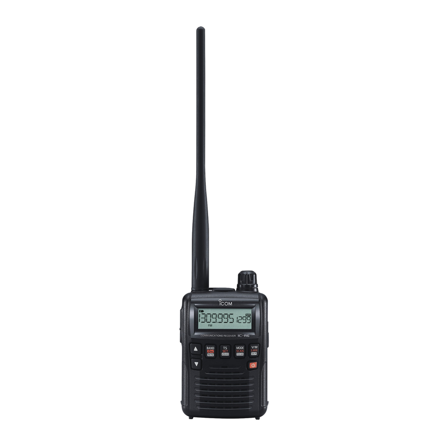
Icom IC-R6 Service Manual
Communications receiver
Hide thumbs
Also See for IC-R6:
- Instruction manual (96 pages) ,
- Price list (158 pages) ,
- Instruction manual (40 pages)
Table of Contents
Advertisement
Quick Links
Advertisement
Table of Contents

Subscribe to Our Youtube Channel
Related Manuals for Icom IC-R6


Summary of Contents for Icom IC-R6
- Page 1 COMMUNICATIONS RECEIVER S-14622XZ-C1 Feb. 2010...
- Page 2 6. READ the instructions of test equipment throughly before connecting a test equipment to the receiver. Icom, Icom Inc. and the Icom logo are registered trademarks of Icom Incorporated (Japan) in Japan, the United States, the United Kingdom, Germany, France, Spain, Russia and/or other countries.
-
Page 3: Table Of Contents
TABLE OF CONTENTS SECTION SPECIFICATIONS SECTION INSIDE VIEWS SECTION DISASSEMBLY INSTRUCTION SECTION CIRCUIT DESCRIPITON RECEIVER CIRCUITS (RF UNIT)..........4-1 AF CIRCUITS (LOGIC UNIT) . -
Page 4: Specifications
SECTION 1. SPECIFICATIONS GENERAL RECEIVER • Frequency coverage (Unit: MHz) • Receive system : Triple-conversion superheterodyne 0.100–821.995, • Intermediate frequencies : 1st 266.7 MHz 851.000–866.995, 2nd 19.65 MHz (FM/AM) 896.000–1309.995 19.95 MHz (WFM) France 0.100–29.995, 450 kHz (FM/AM) 50.200–51.200, 750 kHz (WFM) 87.500–107.995, 144.000–146.000, •... -
Page 5: Logic Unit
SECTION 2. INSIDE VIEWS • LOGIC UNIT (TOP VIEW) (IC1) VOLTAGE LIMITER (D511) LOGIC3.3V REGULATOR (Q103) TONE FILTER IFV LINE SW (IC200) (Q104) +5 V REGULATOR (IC455) +3 V REGULATOR (IC104) RESET (IC3) 2 - 1... - Page 6 • LOGIC UNIT (BOTTOM VIEW) ELECTRIC VOLUME (IC451) AF MUTE SW (Q350) EEPROM (IC2) REGULATOR FOR AF AMP CI-V LEVEL CONVERTER (IC454) (IC452) SPEAKER MUTE SW AF PRE-AMP (Q507) (Q300) AF FILTER AF POWER AMP (Q301) (IC450) WIDE/NARROW MODE SW +3S LINE REGULATOR (Q302) (Q102)
- Page 7 • RF UNIT (TOP VIEW) 1st IF FILTER (FI1) ATTENUATOR (D68) 2nd IF MIXER ATTENUATOR DRIVER (Q523) (Q521) 1st IF MIXER BAR ANTENNA (IC1) TUNING DIODE (D100) IF DEMODULATOR IC (IC12) RF AMP NOISE AMP (Q505) (IC13) BAR/EXTERNA WFM/FM ANTENNA SW MODE SW (Q510) (D55)
-
Page 8: Disassembly Instruction
3) Remove the rear panel in the direction of the arrow. front panel. (NOTICE: The latch falls off when removing the rear 2) Unsolder the 2 points from the speaker. panel.) SCREW Remove with; “ICOM Driver (Q)” UNSOLDER REAR PANEL (8960000370) DIAL KNOB ANT NUT Solder... -
Page 9: Circuit Descripiton
SECTION 4. CIRCUIT DESCRIPTION 4-1 RECEIVER CIRCUITS (RF UNIT) EARPHONE ANTENNA • 15–29.995 MHz When using the connected earphone as an antenna, RX The RX signal from the antenna connector (CHASSIS; J1) signal from the earphone is applied to the RF circuits (except is applied to the RF AMP (Q505) through the band SWs 0.10–1.895 MHz band), through the earphone antenna SW (D63, D64 and D73), LPF and the HPF. - Page 10 1ST IF CIRCUIT (RF UNIT) 3RD IF AND DEMODULATOR CIRCUITS The RX signal from the RF circuit is applied to the 1st IF (RF UNIT) mixer (IC1) to be mixed with the 1st LO signal from the 1st The signal from the 2nd IF AMP (Q5) is applied to the IF de- LO VCO (Q528, Q529, D105 and D106), resulting in the modulator IC (IC12) which contains the 3rd IF mixer, 3rd IF 266.7 MHz 1st IF signal.
-
Page 11: Af Circuits (Logic Unit)
DOUBLER CIRCUITS FOR THE 1ST LO SIGNAL The amplified AF signal is passed through the LPF (R350 IC-R6 has two doubler circuits, "DBL1" and "DBL2". They and C404), whose frequency response is changed by Q508 double the frequency of the VCO output signal to obtain the according to the user setting (The "AF FILTER"). -
Page 12: Voltage Block Diagrams
4-4 VOLTAGE BLOCK DIAGRAM 4-5 CPU PORT ALLOCATION Voltage from the power supply is routed to throughout the Line Description transceiver via regulators and switches. Name IOCK Expand IC serial clock. IC103 IOSTB Expand IC strobe. IOEN Expand IC chip enable. IODATA Expand IC serial data. - Page 13 L=While in the power save mode. Doubler circuit (DBL1; Q31, D44, D47) control. DBL2 L= While receiving 494.2–833 MHz and 1066.7–1309.995 MHz. Main power swtich (LOGIC UNIT: PCON Q103) control. L=IC-R6 is power ON. +3S line control. +3SC L=Receiving. 4 - 5...
-
Page 14: Adjustment Procedures
SECTION 5. ADJUSTMENT PROCEDURE 5-1 PREPARATION ¤ REQUIRED EQUIPMENTS EQUIPMENT GRADE AND RANGE EQUIPMENT GRADE AND RANGE Modifi ed 3-conductor 3.5 (d) mm plug JIG cable (See the illust below) Frequency range : 100 kHz to 1.2 GHz Standard signal Output level : –20 to +107 dBµ... -
Page 15: Frequency Adjustment
5-2 FREQUENCY ADJUSTMENT 1) Select an adjustment item using [BAND]/[TS]. 2) Set or modify the adjustment value as specifi ed using [DIAL], then push [V/M] to store the adjustment value.. RECEIVER’S ADJUSTMENT ADJUSTMENT OPERATION VALUE CONDITION ITEM REFERENCE 1 • Frequency: 439.800 MHz • Connect a frequency counter to "2nd 247.050 MHz FREQUENCY LO"... -
Page 16: Receive Adjustments
: 0.495 MHz Level : 107 dBµ (0 dBm) Modulation : None Push [V/M] 2) Gradually move the IC-R6 away from (the 11th the SG until the 11th scale of the scale is just signal strength indicator on the IC-R6 disappeared) LCD disappears. - Page 17 5-3 RECEIVE ADJUSTMENTS (Continued) 1) Select an adjustment item using [BAND]/[TS]. 2) Set the SSG as specifi ed, then push [V/M] to store the adjustment value. RECEIVER’S ADJUSTMENT ADJUSTMENT OPERATION VALUE CONDITION ITEM VHF SENSITIVITY 1 • Frequency: 118.100 MHz •...
- Page 18 5-3 RECEIVE ADJUSTMENTS (Continued) 1) Select an adjustment item using [BAND]/[TS]. 2) Set the SSG as specifi ed, then push [V/M] to store the adjustment value. RECEIVER’S ADJUSTMENT ADJUSTMENT OPERATION VALUE CONDITION ITEM S-METER 1 NOTE: "SENSITIVITY" must be adjusted before "S-METER." And when "SENSITIVITY" is re- adjusted, "S-METER"...
-
Page 19: Parts List
SECTION 6. PARTS LIST [RF UNIT] [RF UNIT] PARTS PARTS DESCRIPTION DESCRIPTION LOCATION LOCATION 1110005230 S.IC UPC2757TB-E3 29.3/24.8 2040001200 S.SAW EFCH266MKQP1 35.9/30.1 1130012930 S.IC MB15F63ULPVA1-G 25.6/6 2020002410 CER LTM450FW <JJE> IC12 1110007300 S.IC NJM2552V-TE1-#ZZZB 44.8/20.2 2010002280 S.MON 19S15A 19.650 MHz(FL-293) 36.8/31.1 IC13 1110006490 S.IC... - Page 20 [RF UNIT] [RF UNIT] PARTS PARTS DESCRIPTION DESCRIPTION LOCATION LOCATION L110 6200011031 S.COI ELJRF R10JFB 8.5/8.9 R240 7030005120 S.RES ERJ2GEJ 102 X (1K) 7.6/22.5 L111 6200007881 S.COI ELJRF 33NJFB 3.4/4.3 R241 7030005120 S.RES ERJ2GEJ 102 X (1K) 4.3/18.2 R243 7030005090 S.RES ERJ2GEJ 104 X (100K) 3.4/20.6 R245 7030005220 S.RES ERJ2GEJ 223 X (22K)
- Page 21 [RF UNIT] [RF UNIT] PARTS PARTS DESCRIPTION DESCRIPTION LOCATION LOCATION 4030017730 S.CER C1005 JB 1H 471K-T 27.3/38.3 C267 4030017360 S.CER C1005 CH 1H 030B-T 14/17.3 4030017460 S.CER C1005 JB 1H 102K-T 22.5/36.9 C410 4030017460 S.CER C1005 JB 1H 102K-T 11.7/25.4 4030017460 S.CER C1005 JB 1H 102K-T 14.2/31.5 C414...
-
Page 22: Logic Unit
[RF UNIT] [LOGIC UNIT] PARTS PARTS DESCRIPTION DESCRIPTION LOCATION LOCATION C716 4030017550 S.CER C1005 CH 1H 1R5B-T 12.5/21.7 1140015260 S.IC UPD78F1508AGF(R)-GAT-AX 20.1/25 C719 4030016790 S.CER C1005 JB 1E 103K-T 40.1/8.4 1130012691 S.IC R1EX24256ASA00A 9.8/17.9 C720 4030017350 S.CER C1005 CH 1H 020B-T 4.7/4.2 1110005821 S.IC R3112N281A-TR-F... - Page 23 [LOGIC UNIT] [LOGIC UNIT] PARTS PARTS DESCRIPTION DESCRIPTION LOCATION LOCATION 7030005120 S.RES ERJ2GEJ 102 X (1K) 15.5/10.6 R533 7030005240 S.RES ERJ2GEJ 473 X (47K) 28.4/42.5 7030005240 S.RES ERJ2GEJ 473 X (47K) 16.5/11.3 R538 7030005060 S.RES ERJ2GEJ 333 X (33K) 25.2/20.3 7030005170 S.RES ERJ2GEJ 474 X (470K) 17.6/10.8 R542...
- Page 24 [LOGIC UNIT] PARTS DESCRIPTION LOCATION C351 4030016930 S.CER C1005 JB 1A 104K-T 19.5/22.1 C352 4030016930 S.CER C1005 JB 1A 104K-T 18.6/18.9 C400 4030016930 S.CER C1005 JB 1A 104K-T 19.7/25.6 C402 4030016930 S.CER C1005 JB 1A 104K-T 26.1/20.1 C403 4030017490 S.CER C1608 JB 1A 105K-T 33.9/7.5 C404 4030017780 S.CER C1005 JB 1H 472K-T...
-
Page 25: Rf Unit
SECTION 7. MECHANICAL PARTS [CHASSIS PARTS] [RF UNIT] ORDER ORDER DESCRIPTION QTY. DESCRIPTION QTY. 6510020121 AXK6S40547YG 6510027770 3250 ANT CONNECTOR 3310003010 KY-058-006-2 2510001550 K036NA511-10 MP1* 8510019650 3250 VCO CASE 8210026020 3250 FRONT PANEL (incl. MP9) 8510019660 3250 VCO COVER 8210026030 3250 REAR PANEL 8510019680 3250 RF B-SHIELD 8110009931 1995 BATT COVER (B)-1 MP8*... - Page 26 MP3(C) MP26(C) MP15(C) MP19(C) MP14(R) MP23(C)×2 MP24(C)×2 MP30(C) MP2(C) MP22(C) MP18(C) EP2(R) MP15(R) MP17(C) MP2(R)×3 MP13(R) MP24(C)×2 RF UNIT MP31(C) MP8(C) MP5(R) MP11(R) MP12(R) MP5(L) MP2(R)×3 MP12(C) MP20(C) W1(L) MP13(C) J1(C) MP16(R) MP7(L) MP10(L) S9(L) S6(L) MP22(C)×2 MP3(L) MP4(L)×2 MP6(C) MP9(L) MP2(L) DS1(L)
- Page 27 The combination of top side and bottom side of this SECTION 8. BOARD LAYOUTS • LOGIC UNIT (TOP VIEW) R551 R512 R549 R550 • RF UNIT (TOP VIEW) R553 J500 R400 EP21 EP20 R383 R110 R232 C542 R556 C141 C666 L107 C673 D511...
- Page 28 The combination of top side and bottom side of this [DIAL] • LOGIC UNIT [SP] (BOTTOM VIEW) EP16 D504 EP11 R505 C452 ANT CONNECTOR R524 J1 (CHASSIS) R525 R506 R508 IC454 EP10 R507 IC452 R523 C515 C507 R401 R302 C304 [FUNC] Q507 R304...
- Page 29 SECTION 9. BLOCK DIAGRAM ANT CONNECTOR J1(CHASSIS) ANTENNA RF UNIT 0.10-1.895 MHz Q506:LDTA144 300MC 300MC VHFC 300M2V LEVEL UHFC CONV TUNE TRAC Q501:UNR9114 LOGIC3.3V 800MC Q521:LDTA144 D100:SVC389 Q513:XP4601 D68:1SV172 D 54:MA2S111 ANTSW UHFC UHF2V VHFC I OEN VHF2V Q504:XP1113 Q502:XP1114 IOSTB,IOCK,IODATA,IOEN 0.10-1.895 MHz EARPHONE...
- Page 30 EAR ANT LOGIC UNIT SP1(CHASSIS) I C454:NJU7775F3 2 LOGIC3.3 AFON Q511 AF-V LDTC144 Q505:2SA1832 VR_DATA IC451:SM6451 VR_CLK AFON VR_STB AM P MUTE IC450:TS4990 Q507:SSM3K01T D505:1SS400 EXT SP Q301:XP6501 D300:MA2S1110G Q350:2SJ144 M ODE AMUTE MUTE AF FIL AF-V AF_SEL Q508:LDTC144 AF_FIL AF_FIL AM P CTRL...
- Page 31 SECTION 10. VOLTAGE DIAGRAM LOGIC UNIT (1/2) *R3 *R5 3 . 3 3 V 0.001 0.001 MMZ1005Y102C T EP17 +3.3CPU VR_DATA VR_CLK 2.99V TEST2 2SA1832 CP10S TEST1 C116 Q102 CP10S 470k R104 C120 0.001 LDTC144EE CSTCE12M2G52 SEG27 SEG26 TAK-35455 0.01 SEG25 LOGIC3.3V SEG24...
- Page 32 LOGIC UNIT (2/2) +3.3CPU 4 . 7 9 V O N : 3 . 3 1 V O F F : 0 . 0 0 V 2SC4738 R558 R559 O N : 2 . 6 4 V LOGIC3.3V O F F : 0 . 3 3 V C128 47 MSVA DBL2...
- Page 33 RF UNIT (1/2) Bar ANT Ext.ANT MA2S077G0 R241 R247 ANTS W CP10S SVC389 C566 D100 Q510 R245 C568 C571 CP10S 0.01 1 3 . 2 V CP10S CP10S 0.001 C567 Q513 XP4601 Q506 R240 C569 C536 LDTA144EE UMD6 Q527 2 . 8 4 V TRAC 2SA1832 R329...
- Page 34 RF UNIT (2/2) LOGIC3.3V R319 R320 LQW18AN5N6C00 2 . 6 5 V DBL2 C510 D BL1 L QW18AN8N2D00 C258 5.6N R197 SHIFT 0.001 TRAC L111 C256 C727 R321 0.00 1 *C160 2 . 0 8 V C237 0.001 0 . 7 0 V 2 .
- Page 35 Highway 17 Delta, B.C., V4K 5B8, Canada : http://www.icomspain.com Phone : +1 (604) 952-4266 Fax : +1 (604) 952-0090 E-mail : icom@icomspain.com : http://www.icomcanada.com E-mail : info@icomcanada.com Blacksole House, The Boulevard, Altira Business Park, Herne Bay, CT6 6GZ, UK Phone : +44 (01227) 741741...
- Page 36 S-14622XZ-C1 1-1-32, Kamiminami, Hirano-ku, Osaka 547-0003, Japan © 2010 Icom Inc.
Need help?
Do you have a question about the IC-R6 and is the answer not in the manual?
Questions and answers