Denon S-101 Service Manual
Hide thumbs
Also See for S-101:
- Service manual (140 pages) ,
- Operating instructions manual (138 pages) ,
- Brochure & specs (9 pages)
Table of Contents
Advertisement
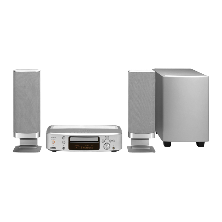
HOME THEATER SYSTEM (S-101) consists of DVD SURROUND RECEIVER (ADV-S101)
and SUB WOOFER (DSW-S101) and SPEAKER SYSTEM (SC-S101)
For purposes of improvement, specifications and
●
design are subject to change without notice.
Please use this service manual with referring to the
●
operating instructions without fail.
Some illustrations using in this service manual are
●
slightly different from the actual set.
SERVICE MANUAL
MODEL
DVD HOME THEATER SYSTEM
TOKYO, JAPAN
Denon Brand Company, D&M Holdings Inc.
S-101
注 意
サービスをおこなう前に、このサービスマニュアルを
必ずお読みください。本機は、火災、感電、けがなど
に対する安全性を確保するために、さまざまな配慮を
おこなっており、また法的には「電気用品安全法」に
もとづき、所定の許可を得て製造されております。
従ってサービスをおこなう際は、これらの安全性が維
持されるよう、このサービスマニュアルに記載されて
いる注意事項を必ずお守りください。
本機の仕様は性能改良のため、予告なく変更すること
●
があります。
補修用性能部品の保有期間は、製造打切後8年です。
●
修理の際は、必ず取扱説明書を参照の上、作業を行っ
●
てください。
本文中に使用しているイラストは、説明の都合上現物
●
と多少異なる場合があります。
For U.S.A., Canada
& Europe model
Ver. 1
X0244 V.01 DE/CDM 0507
Advertisement
Table of Contents

Related Manuals for Denon S-101


Summary of Contents for Denon S-101
- Page 1 For U.S.A., Canada & Europe model Ver. 1 SERVICE MANUAL S-101 MODEL DVD HOME THEATER SYSTEM HOME THEATER SYSTEM (S-101) consists of DVD SURROUND RECEIVER (ADV-S101) and SUB WOOFER (DSW-S101) and SPEAKER SYSTEM (SC-S101) 注 意 サービスをおこなう前に、このサービスマニュアルを 必ずお読みください。本機は、火災、感電、けがなど に対する安全性を確保するために、さまざまな配慮を おこなっており、また法的には「電気用品安全法」に...
-
Page 2: Laser Radiation
S-101 SAFETY PRECAUTIONS The following check should be performed for the continued protection of the customer and service technician. LEAKAGE CURRENT CHECK Before returning the unit to the customer, make sure you make either (1) a leakage current check or (2) a line to chassis resistance check. - Page 3 S-101 RDISASSEMBLY 各部のはずしかた (Follow the procedure below in reverse order when (組み立てるときは、逆の順序でおこなってください。 ) reassembling.) 1. Loader Panel 1. ローダーパネルのはずしかた (1) Switch on, and press [ (OPEN/CLOSE)] button (1) 電源を入れ「 (OPEN/CLOSE)」ボタンを押して、 to open the Disc tray. ディスクトレイを開きます。 (2) Detach the Loader Panel by lifting.
- Page 4 S-101 3. Top Cover 3. トップカバーのはずしかた (1) Remove 9 top screws, then detach Top Cover. (1) トップカバーを止めている上部のネジ 9 本をはず し、トップカバーを矢印の方向へはずします。 4. フロントパネルのはずしかた 4. Front Panel Ass’y (1) フロントパネルからの基板とシャーシを止めてい (1) Remove 3 Front panel screws, then detach P.W.B. るネジを 3 本はずします。...
- Page 5 S-101 Special operating procedures 特殊操作方法 1. Initialization 1. 初期化 This initializes the data for the function, volume, ※ ファンクション、VOL 及び DVD メカ (RL-874) 等の ※ DVD mechanism (RL-874), etc. データを初期化します。 (1) Check that the AC cord is disconnected from the (1) AC コードがコンセントより外れていることを確認...
- Page 6 S-101 ADJUSTMENT 調整 1. SETTING 1. セッティング手順 (1) Connect the oscilloscope to the Y-signal, P -signal and (1) セットの ZONE2 COMPONENT OUT の端子(Y, P )をそれぞれオシロスコープ(終端抵抗:75Ω) -signal, P -signal and C -signal of ZONE2 COMPO- に接続します。 NENT OUT terminal and each terminate at 75 Ohms.
- Page 7 S-101 2.4. Procedure 2.4. 手順 (1) Adjust the signal of COMPONENT OUT by the wave of (1) COMPONENT OUT の信号レベルをオシロスコープ上の oscilloscope. 波高値で調整します。 (a) Y 信号レベル (a) Target, Y-signal 調整個所 : 1U-3695-3 VR601 Point 1U-3695-3 VR601 調整値 : 714 ± 35mV Adjustment Value 714 ±...
- Page 8 S-101 BLOCK DIAGRAM DATP20:FL/FR DAIP19:C/SW DAIP18:SL/SR DAIP16:FL/FR DAIP16:0/SW DAIP15:0/0 DAIP14:RECL/RECR...
-
Page 9: Level Diagram
S-101 LEVEL DIAGRAM... - Page 10 S-101 SEMICONDUCTORS / 半導体一覧表 Only major semiconductors are shown, general semiconductors etc. are omitted to list. 主な半導体を記載しています。汎用の半導体は記載を省略しています。 1. IC’s ES6128F (RL-S874: U9) DSCK DSCK AUX[0] AUX[0] AUX[1] AUX[1] DCS0# DCS0# AUX[2] AUX[2] DCS1# DCS1# AUX[3] AUX[3] DB15 DB15 AUX[4] AUX[4]...
- Page 11 S-101 Pin No. Pin Name Function RESET# Reset input, active low. TDMDX TDM transmit data. TDMDR TDM receive data. TDMCLK TDM clock input. TDMFS TDM frame sync. TDMTSC# TDM output enable. Audio transmit frame sync. SEL_PLL2 System and DSCK output clock frequency selection is made at the rising edge of RESET#.
- Page 12 S-101 Pin No. Pin Name Function VDAC Video VDAC output. YUV7 YUV7 pixel output data. PCLK2XSCN 27 MHz video output pixel clock. PCLKQSCN 13.5 MHz video output pixel clock. VSYNC# Vertical sync, active low. HSYNC# Horizontal sync, active low. 127:122 HD[5:0] Host data I/O [5:0].
- Page 13 S-101 M5705 (RL-S874: U1) AVSS-DS XRD(3) XSRFIN XRD(12) XSIPIN AVDD5-DS XRD(2) XRD(13) XSDSSLV XSRSLINT XRD(1) XRD(14) XSAWRC XRD(0) XRD(15) XSRFGC XSEFGC XHD(7) XSFOCUS XHD(8) XSTRACK XHD(6) XSSLEG XHD(9) AVDD5-DA XHD(5) XSMOTOR XHD(10) AVSS-DA XHD(4) XSRFRPLP XHD(11) XSTELP XSVREF2 XHD(3) XSRFRP...
- Page 14 S-101 Pin No. Type Description Pin Name XSSBAD Sub-beam addition signal input Phase detector reference current generator. Connect a resistor between this pin and XSPDIREF ground to set reference current Frequency detector reference current generator. Connect a resistor between this pin and...
- Page 15 S-101 Pin No. Type Description Pin Name XHPDIAGJ This pin is used as the Passed Diagnostics signal, and may be an input or an open-drain output This pin is used as the Drive Active/Slave Present signal, and is an input or an open-drain XHDASPJ output.
- Page 16 S-101 M30627FHPGP (IC202: 1U-3694) Port Port Port Name Explanation Function setting VREF VREF Reference Voltage Input for A/D converter AVcc AVcc Positive power SIN4 FL_CS Chip Enable output to FLD SOUT4 FL_DA Serial Data output to FLD CLK4 FL_CK Serial Clock output to FLD...
- Page 17 S-101 Port Port Port Name Explanation Function setting NC(L:Output) Not Used: N. C. NC(L:Output) Not Used: N. C. RXD2 NC(L:Output) Not Used: N. C. TXD2 NC(L:Output) Not Used: N. C. TXD1 USB/IPOD_TXD Serial Data output to USB/IPOD VCC1 Positive power...
- Page 18 S-101 Port Port Port Name Explanation Function setting /INT3 REMOTE Remote Control signal input Reset output to RDS IC DIR DOUT Serial Data input from DIR. DIR/CODEC DIN Serial Data output to DIR. DIR/CODEC CLK Serial Clock output to DIR.
- Page 19 S-101 ADSP-21266SKSTZ-1C (IC906: 1U-3694) PIN 1 INDICATOR TOP VIEW ADSP-21266SKSTZ-1C Terminal Function LQFP LQFP LQFP LQFP Pin Name Pin # Pin Name Pin # Pin Name Pin # Pin Name Pin # DDINT DDINT DDEXT CLKCFG0 DDINT CLKCFG1 DDINT BOOTCFG0...
-
Page 20: Top View
S-101 SP3721A (RL-S874: U2) DVDRFP SDEN DVDRFN SDATA SCLK TOP VIEW MEVO MLPF SP3721A Terminal Function Pin No. Type Description Pin Name 1, 2 DVDREP , DVDREN RF Signal Inputs. Differential RF signal attenuator input pins CDRF RF Signal Inputs. Single-ended RF signal attenuator input pin... - Page 21 S-101 Pin No. Pin Name Type Description Center Error Signal Output. Center error output reference to VCI NEVO SIGO Bottom Envelope Output. Bottom envelope for mirror detection Defect Output. Pseudo CMOS output. When a defect is detected, the DFT output goes high. Also the servo AGC output can be monitored at this pin, when CAR bits 7-4 are ‘0011’...
- Page 22 S-101 TAS5066 (IC805: 1U-3683) 64 63 62 61 60 59 58 57 56 55 54 53 52 51 50 49 DVDD_RCL MCLK_IN DVSS_RCL AVDD_PLL PLL_FLT_OUT DVDD_PWM PLL_FLT_RET DVSS_PWM AVSS_PLL PWM_AP_4 PWM_AM_4 DVSS1 VALID_4 PWM_AP_5 ERR_RCVRY PWM_AM_5 MUTE VALID_5 PWM_AP_6 PWM_AM_6...
-
Page 23: Block Diagram
S-101 M66005-0001AHP (IC301: 1U-3681) SEG02 SEG19 SEG01 SEG20 SEG21 SEG00 Vcc2 SEG22 SEG23 DIG15/SEG39 SEG24 DIG14/SEG38 SEG25 DIG13/SEG37 SEG26 DIG12/SEG36 M66005-0001AHP DIG11 DIG10 SEG27 DIG09 SEG28 SEG29 DIG08 DIG07 SEG30 SEG31 DIG06 DIG05 SEG32 SEG33 DIG04 BLOCK DIAGRAM Display code RAM ・... - Page 24 S-101 AD1837 (IC711: 1U-3694) DVDD DVDD CLATCH DBCLK DLRCLK PD/RST AGND AGND OUTR4 TOP VIEW OUTL1 OUTL4 OUTR1 AGND AGND AVDD AVDD OUTR3 OUTL2 DVDD DVDD ODVDD ALRCLK ABCLK ASDATA CCLK CLATCH COUT MCLK PD/RST M/S AVDD AVDD DLRCLK CONTROL PORT...
-
Page 25: Pin Description
S-101 HY57V651620BTC-75 (RL-S874: U11) DQ 0 DQ15 DQ 1 DQ14 DQ 2 DQ13 DQ 3 DQ12 DQ 4 DQ 11 DQ 5 DQ10 DQ 6 DQ 9 DQ 7 DQ 8 LDQM /W E UD QM /CAS /RAS A10/A P... - Page 26 S-101 T431616A-8S(RL-S874:U5) DQ15 DQ14 DQ 2 DQ13 DQ 3 DQ12 DQ 4 DQ11 DQ 5 DQ10 DQ 6 DQ 9 DQ 7 DQ 8 LDQM N.C / RFU UD QM CL K CK E A10/AP PIN DESCRIPTION PIN NAME DESCRIPTION Active on the positive going edge to sample all input.
- Page 27 S-101 MX29LV800ABTC-70 (RL-S874: U10) BYTE Q15/A-1 RESET RY/BY BLOCK DIAGRAM WRITE CONTROL PROGRAM/ERASE STATE INPUT HIGH VOLTAGE MACHINE LOGIC RESET (WSM) STATE REGISTER ADDRESS FLASH ARRAY LATCH ARRAY A0-A19 SOURCE COMMAND DATA BUFFER Y-PASS GATE DECODER SENSE COMMAND DATA AMPLIFIER...
- Page 28 S-101 LC89057W (IC707: 1U-3694) EMPHA/UO AUDIO/VO XMODE Microcontroller RXOUT C bit, U bit 37 DO 36 RERR 24 SDIN 23 SLRCK Input Demodulation 22 SBCK Data Selector 21 RDATA & Selector 21 RDATA Lock Detect XMODE 20 RLRCK RX5/VI DGND...
- Page 29 S-101 Pin Name Function XOUT X’tal osc. connecting output terminal X’tal osc. connection, external clock input terminal (24.576MHz or 12.288MHz) DVDD — Digital power DGND — Digital GND EMPHA/UO Emphasis information/U-data output/Chip address setting terminal AUDIO/VO Non-PCM detect/V-flag output/ Chip address setting terminal...
- Page 30 S-101 LH28F800BJE (IC907: 1U-3694) CY7C1049CV-33-10ZC (IC908, 910: 1U-3694) Top View INPUT BUFFER 512K x 8 ARRAY POWER COLUMN DOWN DECODER TA1270BF (IC501: 1U-3695) TC90A69F (IC503: 1U-3695) DAC2 Y OFFSET C BUS PEDESTAL PEDESTAL TEST CONTROL CLAMP CLAMP DAC1 SW GND...
- Page 31 S-101 TAS5121 (IC201, 301, 401: 1U-3683) GVDD_B PWM_BP GVDD_B RESET BST_B DREG_RTN PVDD_B GVDD PVDD_B OUT_B DREG OUT_B DGND OUT_A DVDD OUT_A PVDD_A DGND PVDD_A BST_A PWM_AP GVDD_A GVDD_A Terminal Functions TERMINAL FUNCTION (1) FUNCTION (1) DESCRIPTION DESCRIPTION NAME BST_A...
- Page 32 S-101 BH7868FS (IC301, 302: 1U-3695) 6MHz Vcc1 COUT 75Ω S-DCOUT S-DCOUT 6MHz 75Ω CVOUT Bias CVOUT MUTE1 MUTE1 6MHz CVIN 75Ω Clamp YOUT SEL (CV/MIX) YOUT SAG Clamp 12MHz BIAS Bias 75Ω Py/G OUT Py/G OUT SAG SEL (BIAS/CLAMP) Bias...
- Page 33 S-101 NJM2596 (IC509: 1U-3695) SN74LV573APW (IC903, 904: 1U-3694) PCM1803 (IC803, 804: 1U-3683) MODE1 MODE0 FMT1 FMT0 AGND SCKI PDWN BYPAS DGND TEST DOUT LRCK BLOCK DIAGRAM DeltaœSigma Modulator LRCK DOUT Serial ψ1/64 , ψ1/128 Interface Decimation Reference Filter With Mode/ HighœPass Filter...
- Page 34 S-101 QT240 (IC306: 1U-3681) 1-1 P - QT240-ISS ABLE ISTING Name Description SNS2 Sense pin (to Rs2 + Cs2) SNS2K Sense pin (to Cs2, electrode) SNS2 SNS3K SNS1 Sense pin (to Rs1 + Cs1) SNS2K SNS3 SNS1K Sense pin (to Cs1, electrode); speed option...
- Page 35 S-101 BU4053BCF (IC510: 1U-3695) BU4052BCF (IC518: 1U-3695) YOUT COMMON Y XOUT COMMON X TC74VHC74FT (IC703: 1U-3694) NJM2274R (IC502: 1U-3695) VIEW Power Save CTL Vref Clamp Disc. Bias C Mute CTL BR93L86RFVM-WTR (IC201: 1U-3694) DE T E C T S UP P LY...
- Page 36 S-101 BD9781HFP (IC810: 1U-3695) EN/SYNC 5~35V ON/OFF L:OFF H:ON 1μF 220μF Vref SYNC SOFT START 24KΩ B D 9 7 8 1 H V F P ERROR AMP COMPARATOR DRIVER LATCH 33μH 10KΩ 150KΩ RESET Vref 330μF 4700μF CURRENT LIMIT 390KΩ...
-
Page 37: Pin Function
S-101 STR-F6238S (IC902: 1U-3682: E3) STR-F6267S (IC902: 1U-3682: E2) DR V .R E G O.V .P Latch S tart R g2 R g3 R g1 R eg. FRONT DR V VIEW T .S .D. G ND O.C .P O.C .P O.L.P... - Page 38 S-101 NJM7912FA (IC807: 1U-3695) (IC905: 1U-3682) SE-B2 (IC908: 1U-3682) FRONT FRONT VIEW VIEW 1 REF NJM78L07UA (IC512: 1U-3694) NJM79L07AU (IC513: 1U-3694) COMMON NJM7805FA (IC712: 1U-3694) (IC801: 1U-3695) NJM7812FA (IC806: 1U-3695) (IC909: 1U-3682) BA033T (IC904: 1U-3682) BA05T (IC907: 1U-3682) LM2990T-5.0 (IC809: 1U-3695) LM2940CT-5.0 (IC808: 1U-3695)
- Page 39 S-101 2. FL DISPLAY 15-BT-102GN Pin Connection Grid Assigment Anode Connection...
-
Page 40: Printed Wiring Boards
S-101 PRINTED WIRING BOARDS 1U-3694 MAIN P.W.B. UNIT COMPONENT SIDE... - Page 41 S-101 FOIL SIDE...
- Page 42 S-101 1U-3695 I/F P.W.B. UNIT COMPONENT SIDE...
- Page 43 S-101 FOIL SIDE...
- Page 44 S-101 1U-3681 DISPLAY P.W.B. UNIT COMPONENT SIDE...
- Page 45 S-101 FOIL SIDE...
- Page 46 S-101 1U-3682 SMPS P.W.B. UNIT COMPONENT SIDE...
- Page 47 S-101 FOIL SIDE...
- Page 48 S-101 1U-3683 AMP P.W.B. UNIT COMPONENT SIDE...
- Page 49 S-101 FOIL SIDE...
- Page 50 S-101 MECHANISM P.W.B. UNIT COMPONENT SIDE FOIL SIDE...
-
Page 51: Note For Parts List
S-101 NOTE FOR PARTS LIST 部品表について • Part indicated with the mark "nsp" are not always in stock and possibly to 1.nsp 印の部品は常時在庫していませんので供給に長時間を要すること take a long period of time for supplying, or in some case supplying of part があります。 may be refused. -
Page 52: Parts List Of P.w.b. Unit
S-101 PARTS LIST OF P.W.B. UNIT *本表に記載されている部品は、補修用部品のため製品に使用している部品とは一部、形状、寸法などが異なる場合があります。 * The parts listed below are for maintenance only, might differ from the parts used in the unit in appearances or dimensions. * "nsp" 印の部品は常時在庫していませんので供給に長時間を要することがあります。場合によっては、供給をお断りする場合があります。 * Part indicated with the mark “nsp” are not always in stock and possibly to take a long period of time for supplying, or in some case supplying of part may be refused. - Page 53 S-101 Ref. No. Part No. Part Name Remarks Q'ty New TR213 00D 269 0192 902 KRC102S-RTK(10K-10K) +C TR501,502 00D 275 0100 902 2SK771-5-TB TR503 00D 273 0485 906 KRC107S-RTK(10K-47K) TR504 00D 269 0184 907 KRA102S-RTK TR505-509 00D 273 0460 905...
- Page 54 S-101 Ref. No. Part No. Part Name Remarks Q'ty New CAPACITORS GROUP C101,102 00D 257 0501 901 CK73B1H103KT (1608) +1608 C117 00D 257 0509 929 CK73B1H102KT +1608 C118 00D 257 0511 904 CK73F1H103ZT +1608 C119 00D 257 0509 929 CK73B1H102KT...
- Page 55 S-101 Ref. No. Part No. Part Name Remarks Q'ty New C226 00D 257 0512 903 CK73F1E104ZT +1608 C227,228 00D 257 0506 951 CC73CH1H101JT +1608 C229 00D 254 4740 921 CE67W1C470MT(GV) C230 00D 257 0512 903 CK73F1E104ZT +1608 C231 00D 257 0516 954...
- Page 56 S-101 Ref. No. Part No. Part Name Remarks Q'ty New C315-318 00D 256 1058 939 CF93A1H473JT (JL) C319,320 00D 257 0511 917 CK73F1H223ZT +1608 C321,322 00D 254 4742 916 CE67W1V100MT(GV) C401-408 00D 257 0507 934 CC73CH1H221JT +1608 C409-411 00D 247 2018 903...
- Page 57 S-101 Ref. No. Part No. Part Name Remarks Q'ty New C615 00D 257 0501 901 CK73B1H103KT (1608) +1608 C616 00D 254 3088 901 CE67W1C220MBPT(RV) C617 00D 257 0503 925 CC73CH1H100DT +1608 C618 00D 257 0511 917 CK73F1H223ZT +1608 C619 00D 257 0503 925...
- Page 58 S-101 Ref. No. Part No. Part Name Remarks Q'ty New C741 00D 257 0512 903 CK73F1E104ZT +1608 C742 00D 257 0511 904 CK73F1H103ZT +1608 C743 00D 254 4740 976 CE67W1C100MT(GV) C744 00D 254 4742 916 CE67W1V100MT(GV) C745 00D 257 0516 954...
- Page 59 S-101 Ref. No. Part No. Part Name Remarks Q'ty New C903 00D 254 4720 941 CE04W1E470MT(GR) C910 00D 257 0516 954 CK73B1E104KT +1608 C911 00D 257 0509 929 CK73B1H102KT +1608 C912 00D 257 0516 954 CK73B1E104KT +1608 C913 00D 257 0509 929...
- Page 60 S-101 Ref. No. Part No. Part Name Remarks Q'ty New CX211 00D 205 1006 022 21P FFC BASE (P=1) CY091 00D 205 1100 025 9P FFC BASE(P=1) CY151 00D 205 0736 076 15P FFC CON.BASE FB107 00D 235 0147 909 E.FIL(BLM21PG221SN1)+2125...
- Page 61 S-101 00D1U-3695D I/F P.W.B. UNIT ASS'Y (for U.S.A. & Canada model) Ref. No. Part No. Part Name Remarks Q'ty New SEMICONDUCTORS GROUP IC170 00D 263 0896 909 NJM2068MD-TE1 IC301 00D 262 3365 900 BH7868FS IC304 00D 262 2745 903 BU2090F(E2)
- Page 62 S-101 Ref. No. Part No. Part Name Remarks Q'ty New D815 00D 276 0401 905 1SS133T77 (TAPE) D816 00D 276 0773 905 RB501V-40 +2125 D817 00D 276 0827 903 SPB-G54SVR D818 00D 276 0825 905 SFPB-74V ZD301 00D 209 0008 146...
- Page 63 S-101 Ref. No. Part No. Part Name Remarks Q'ty New C527 00D 257 0516 954 CK73B1E104KT +1608 C528 00D 254 4718 908 CE04W1C100MT(GR) C529 00D 254 4722 981 CE04W1H100MT(GR) C530 00D 254 4737 947 CE04W1H010MT(SF) C531 00D 257 0521 907...
- Page 64 S-101 Ref. No. Part No. Part Name Remarks Q'ty New C609 00D 257 0503 941 CC73CH1H120JT +1608 C610 00D 257 0516 954 CK73B1E104KT +1608 C611,612 00D 257 0501 901 CK73B1H103KT (1608) +1608 C613 00D 254 4734 924 CE04W1C220MT(SF) C614 00D 257 0503 941...
-
Page 65: Pin Header
S-101 Ref. No. Part No. Part Name Remarks Q'ty New C839 00D 257 0512 903 CK73F1E104ZT +1608 C840,841 00D 257 0511 904 CK73F1H103ZT +1608 C842 00D 257 0512 903 CK73F1E104ZT +1608 C843,844 00D 254 4716 926 CE04W0J331MT(GR) C845 00D 257 0512 903... - Page 66 S-101 Ref. No. Part No. Part Name Remarks Q'ty New CY161,162 00D 205 1326 061 16P SOCKT(9120) CY173 00D 205 1352 035 17P-FFC-BASE(TOC-J) CY201,202 00D 205 1354 004 20P SOCKT(9120) CY251 00D 205 1355 003 25P DSUB(MALE) FB301-304 00D 247 2018 903...
- Page 67 S-101 00D1U-3695E I/F P.W.B. UNIT ASS'Y (for Europe model) Ref. No. Part No. Part Name Remarks Q'ty New SEMICONDUCTORS GROUP IC170 00D 263 0896 909 NJM2068MD-TE1 IC301,302 00D 262 3365 900 BH7868FS IC304 00D 262 2745 903 BU2090F(E2) IC501 00D 262 3108 002...
- Page 68 S-101 Ref. No. Part No. Part Name Remarks Q'ty New D801 00D 276 0401 905 1SS133T77 (TAPE) D802 00D 276 0824 906 SFPB-64V D805-812 00D 276 0780 901 SFPX-62 D813 00D 276 0401 905 1SS133T77 (TAPE) D814 00D 276 0773 905...
- Page 69 S-101 Ref. No. Part No. Part Name Remarks Q'ty New C359 00D 254 4718 911 CE04W1C220MT(GR) C360 00D 257 0512 903 CK73F1E104ZT +1608 C361-363 00D 257 0504 982 CC73CH1H470JT +1608 C367 00D 254 4722 907 CE04W1H0R1MT(GR) C368 00D 257 0516 954...
- Page 70 S-101 Ref. No. Part No. Part Name Remarks Q'ty New C596 00D 254 4722 952 CE04W1H2R2MT(GR) C597,598 00D 254 4732 942 CE04W0J101MT(SF) C599,600 00D 257 0516 954 CK73B1E104KT +1608 C601 00D 254 4722 952 CE04W1H2R2MT(GR) C602 00D 257 0501 901...
- Page 71 S-101 Ref. No. Part No. Part Name Remarks Q'ty New C817 00D 257 1020 902 CK73B1H105KT C819 00D 254 4709 700 CE04W1V221MC JC5(KY) C820 00D 254 4708 701 CE04W1V471MC J20(KY) C822 00D 255 1280 908 CQ93M2D103JT(B) C823 00D 255 1278 907...
- Page 72 S-101 Ref. No. Part No. Part Name Remarks Q'ty New CX065 00D 205 1072 946 6P PH CON.BASE +REF CX091 00D 205 1100 025 9P FFC BASE(P=1) CX101 00D 205 0375 000 10P CON.BASE(KR-PH) CX141 00D 205 1324 047 14P PIN HEADER(9120)
-
Page 73: Shield Cover
S-101 Ref. No. Part No. Part Name Remarks Q'ty New W802 LUG PLATE X501 00D 399 0810 006 CSB503F30 X502 00D 399 0802 001 XTAL(3.58MHZ) X503 00D 399 0809 004 XTAL(4.43MHZ) INSULATING SHEET 220 for IC808,809 INSULATOR(YC40B) for IC808,809 HEAT SINK (A) - Page 74 S-101 00D1U-3681D DISPLAY P.W.B. UNIT ASS'Y Ref. No. Part No. Part Name Remarks Q'ty New SEMICONDUCTORS GROUP IC301 00D 262 3512 009 M66005-0001AHP IC302 00D 499 0306 001 GP1UE271XK IC303 00D 262 2745 903 BU2090F(E2) IC304 00D 263 1236 908...
- Page 75 S-101 Ref. No. Part No. Part Name Remarks Q'ty New C331 00D 254 4734 911 CE04W1C100MT(SF) C332 00D 257 0509 929 CK73B1H102KT +1608 C333,334 00D 257 0501 901 CK73B1H103KT (1608) +1608 C336 00D 257 0509 929 CK73B1H102KT +1608 C337 00D 257 0512 903...
- Page 76 S-101 Ref. No. Part No. Part Name Remarks Q'ty New JK301 00D 204 8636 010 MINI JACK(ST SW) JK303 00D 204 8636 010 MINI JACK(ST SW) S301-305 00D 212 0467 000 TACT SW(H=5) S306 00D 212 0461 006 ROTARY ENCODER(V)
- Page 77 S-101 00D1U-3682D SMPS P.W.B. UNIT ASS'Y (for U.S.A. & Canada model) Ref. No. Part No. Part Name Remarks Q'ty New SEMICONDUCTORS GROUP IC901 00D 262 3509 708 SI-8120E (LF1101) IC902 00D 265 0116 009 STR-F6238S(LF1351) IC903 00D 268 0073 905...
- Page 78 S-101 Ref. No. Part No. Part Name Remarks Q'ty New C907-909 00D 253 8022 710 CK45F2EAC222MC C910,911 00D 256 8038 004 CF99--2EAC104M C912 00D 253 8022 710 CK45F2EAC222MC C913 00D 255 4261 775 CQ93P2J392KC(ECQP) C914,915 00D 253 8022 710 CK45F2EAC222MC...
- Page 79 S-101 Ref. No. Part No. Part Name Remarks Q'ty New F901 00D 206 1094 066 FUSE(233)T4AL125V F902 00D 206 1094 037 FUSE(233)T2AL125V FF901,902 00D 202 0040 909 FUSE CLIP(TAPE) FH901,902 00D 202 0040 909 FUSE CLIP(TAPE) L901,902 00D 239 0038 049 L.FILTER(HR28R-E822)
- Page 80 S-101 00D1U-3682E SMPS P.W.B. UNIT ASS'Y (for Europe model) Ref. No. Part No. Part Name Remarks Q'ty New SEMICONDUCTORS GROUP IC901 00D 262 3509 708 SI-8120E (LF1101) IC902 00D 265 0118 007 STR-F6267S(LF1351) IC903 00D 268 0073 905 ICP-N15T IC904...
- Page 81 S-101 Ref. No. Part No. Part Name Remarks Q'ty New C907,908 00D 253 8022 710 CK45F2EAC222MC C909 00D 253 8022 723 CK45F2EAC102MC C910,911 00D 256 8038 004 CF99--2EAC104M C912 00D 253 8022 723 CK45F2EAC102MC C913 00D 253 8030 016 CK45B3D102KC(ECKA)
- Page 82 S-101 Ref. No. Part No. Part Name Remarks Q'ty New CY071 00D 205 0233 074 7P EH CONNECTOR BASE CY101 00D 205 0275 003 10P EH CON. BASE F901 00D 206 1096 035 FUSE(218)T2.5AL250V F902 00D 206 1096 022 FUSE(218)T2AL250V...
- Page 83 S-101 00D1U-3683D AMP P.W.B. UNIT ASS'Y Ref. No. Part No. Part Name Remarks Q'ty New SEMICONDUCTORS GROUP IC201 00D 262 3503 908 TAS5121DKDR IC301 00D 262 3503 908 TAS5121DKDR IC401 00D 262 3503 908 TAS5121DKDR IC501-505 00D 263 0615 902...
- Page 84 S-101 Ref. No. Part No. Part Name Remarks Q'ty New C216,217 00D 257 0516 954 CK73B1E104KT +1608 C218 00D 253 1180 921 CK45B1H102KT(DD-3) C301-303 00D 257 0035 901 CK73B1H104KT +2125 C305 00D 257 0024 909 CK73F1C105ZT +2125 C306 00D 257 1011 966...
- Page 85 S-101 Ref. No. Part No. Part Name Remarks Q'ty New C576 00D 257 0511 904 CK73F1H103ZT +1608 C577 00D 257 0509 929 CK73B1H102KT +1608 C578 00D 257 0511 904 CK73F1H103ZT +1608 C579 00D 257 0509 929 CK73B1H102KT +1608 C580 00D 257 0511 904...
- Page 86 S-101 Ref. No. Part No. Part Name Remarks Q'ty New OTHERS PARTS GROUP CX022 00D 205 0581 069 2P VH-VH CON BASE CX031 00D 205 0233 032 3P EH CONNECTOR BASE CX041,042 00D 205 0653 049 4P VH CON.BASE CX043...
- Page 87 S-101 MECHANISM P.W.B. UNIT ASS'Y Ref. No. Part No. Part Name Remarks Q'ty New SEMICONDUCTORS GROUP 00D 943 0011 903 M5705 00D 943 0012 009 SP3721A 00D 943 0012 805 AT49F001N-70JC 00D 943 0012 902 T431616A-8S 00D 943 0013 008...
- Page 88 S-101 Ref. No. Part No. Part Name Remarks Q'ty New CAPACITORS GROUP 00D 943 0015 226 CERAMIC,0.047U (47N),10%,16V 00D 943 0015 174 CERAMIC,560P,10%,50V C4,5 00D 943 0015 255 CERAMIC,0.1U,-20 - 80%,25V 00D 943 0015 132 CERAMIC,47P,5%,50V C7,8 00D 943 0015 255 CERAMIC,0.1U,-20 - 80%,25V...
- Page 89 S-101 Ref. No. Part No. Part Name Remarks Q'ty New 00D 943 0015 271 ELECTROLYTIC,20%,22U/6.3V 00D 943 0015 310 ELECTROLYTIC,20%,220U/6.3V 00D 943 0015 297 ELECTROLYTIC,20%,100U/6.3V TC11,12 00D 943 0015 297 ELECTROLYTIC,20%,100U/6.3V TC13 00D 943 0015 310 ELECTROLYTIC,20%,220U/6.3V TC14,15 00D 943 0015 297 ELECTROLYTIC,20%,100U/6.3V...
-
Page 90: Exploded View
S-101 EXPLODED VIEW E2 oniy WARNING: Parts marked with this symbol have critical characteristics. Use ONLY replacement parts recommended by the manufacturer. 印の部分は安全を維持するために重要 な部品です。従って交換時は必ず指定の 部品を使用してください。... -
Page 91: Parts List Of Exploded View
S-101 PARTS LIST OF EXPLODED VIEW *本表に記載されている部品は、補修用部品のため製品に使用している部品とは一部、形状、寸法などが異なる場合があります。 * The parts listed below are for maintenance only, might differ from the parts used in the unit in appearances or dimensions. * "nsp" 印の部品は常時在庫していませんので供給に長時間を要することがあります。場合によっては、供給をお断りする場合があります。 * Part indicated with the mark “nsp” are not always in stock and possibly to take a long period of time for supplying, or in some case supplying of part may be refused. - Page 92 S-101 Ref. No. Part No. Part Name Remarks Q'ty New 00D 461 1168 036 RUBBER SHEET 00D 146 2414 233 TOP COVER for E2 00D 146 2414 217 TOP COVER for E3 00D 102 0685 006 TOP BRACKET 00D 146 2419 115...
- Page 93 S-101 Ref. No. Part No. Part Name Remarks Q'ty New SCREWS 00D 473 8089 001 3X15 CUP SCREW 00D 475 6006 008 00D 473 7015 005 3X6 CBTS(S)-B 00D 473 7005 073 3X5 CBTS(S)Z 00D 473 7001 048 2.6X8 CBTS (S)-Z...
-
Page 94: Exploded View Of Dvd Mechanism Unit
S-101 EXPLODED VIEW OF DVD MECHANISM UNIT PARTS LIST OF DVD MECHANISM UNIT *本表に記載されている部品は、補修用部品のため製品に使用している部品とは一部、形状、寸法などが異なる場合があります。 * The parts listed below are for maintenance only, might differ from the parts used in the unit in appearances or dimensions. * "nsp" 印の部品は常時在庫していませんので供給に長時間を要することがあります。場合によっては、供給をお断りする場合があります。 * Part indicated with the mark “nsp” are not always in stock and possibly to take a long period of time for supplying, or in some case supplying of part may be refused. - Page 95 S-101 Ref. No. Part No. Part Name Remarks Q'ty New 00D 943 0009 708 BELT 00D 943 0009 300 AY L/MOTOR 00D 943 0009 407 SLIDE, CAM 00D 943 0009 601 GEAR, PULLY 00D 943 0009 805 LEVER, CAM 00D 943 0009 902 P.W.B., LOADING...
- Page 96 S-101 DSW-S101 EXPLODED VIEW WARNING: Parts marked with this symbol have critical characteristics. Use ONLY replacement parts recommended by the manufacturer. 印の部分は安全を維持するために重要 な部品です。従って交換時は必ず指定の 部品を使用してください。...
-
Page 97: Dsw-S101 Parts List Of Exploded View
S-101 DSW-S101 PARTS LIST OF EXPLODED VIEW *本表に記載されている部品は、補修用部品のため製品に使用している部品とは一部、形状、寸法などが異なる場合があります。 * The parts listed below are for maintenance only, might differ from the parts used in the unit in appearances or dimensions. * "nsp" 印の部品は常時在庫していませんので供給に長時間を要することがあります。場合によっては、供給をお断りする場合があります。 * Part indicated with the mark “nsp” are not always in stock and possibly to take a long period of time for supplying, or in some case supplying of part may be refused. - Page 98 S-101 Ref. No. Part No. Part Name Remarks Q'ty New 00D 513 4093 001 DANGEROUS LABEL ★ 00D 203 6629 000 4P EH-EH CON.CORD ★ 00D 204 2993 005 7P EH-EH CON.CORD ★ 00D 204 2994 004 10P EH-EH CON.CORD ★...
-
Page 99: Sc-S101 Exploded View
S-101 SC-S101 EXPLODED VIEW for Lch for Rch SC-S101 PARTS LIST OF EXPLODED VIEW *本表に記載されている部品は、補修用部品のため製品に使用している部品とは一部、形状、寸法などが異なる場合があります。 * The parts listed below are for maintenance only, might differ from the parts used in the unit in appearances or dimensions. * "nsp" 印の部品は常時在庫していませんので供給に長時間を要することがあります。場合によっては、供給をお断りする場合があります。... - Page 100 S-101 Ref. No. Part No. Part Name Remarks Q'ty PACKING E 29-000-349-01 00D 949 0057 402 CABINET R ch CABINET 52-000-182-01 PACKING C 29-000-347-01 PACKING D 29-000-348-01 SOUND ABSORBENT 54-000-152-01 SOUND ABSORBENT 54-000-152-11 INSERT NUTS 71-099-500-01 SPEAKER JACK (R) 45-000-145-11...
-
Page 101: Packing View
S-101 PACKING VIEW DVD SURROUNDRECIEVER ADV-S101 ACCESSORY BOX ASSY SPEAKER SYSTEM SCS101SRM 102 105 SUB WOOFER 106 107 108 MASTER CARTON PARTS LIST OF PACKING & ACCESSORIES *本表に記載されている部品は、補修用部品のため製品に使用している部品とは一部、形状、寸法などが異なる場合があります。 * The parts listed below are for maintenance only, might differ from the parts used in the unit in appearances or dimensions. - Page 102 S-101 Ref. No. Part No. Part Name Remarks Q'ty 00D 503 1511 107 CUSHION (L) for ADV-S101 00D 503 1512 106 CUSHION (R) for ADV-S101 00D 501 2304 003 ACCESSARY BOX for E3 00D 501 2304 016 ACCESSARY BOX for E2...
-
Page 103: Sub Woofer Unit
S-101 WIRONG DIAGRAM (1) S101 DSW S101 SC S101 SC S101 ADV S101 ITEM PART NO. PART NAME 00D 204 6794 006 25P D-SUB CABLE 00D 203 2439 003 SP CABLE ASSY (2) DSW-S101 ADV S101 CX251 TERMINAL UNIT IN/OUT UNIT... - Page 104 S-101 (2) ADV-S101 DSW S101 CY251 LOCAL POWER UNIT TUNER 1U-3695D-1(E3) PACK 1U-3695E-1(E2) CONVERT UNIT CY072(E2) CX162 CX141 CX162 1U-3695D-3(E3) 1U-3695E-3(E2) (Board to (Board to (Board to CX051(E3) Board) Board) Board) I/F BOARD UNIT 1U-3695D-2(E3) 1U-3695E-2(E2) CY033 CX161 (Board to...
- Page 105 S-101 ITEM PART NO. PART NAME 00D 203 5372 002 3P ZH-PH CON.CORD 00D 204 0599 003 6P PH-PH CON.CORD E2 ONLY 00D 204 8567 005 5P PH-PH CON.CORD E3 ONLY 00D 009 0265 004 17P FFC CABLE 00D 204 0570 019...
-
Page 106: Note For Schematic Diagram
S-101 NOTE FOR SCHEMATIC DIAGRAM 配線図について WARNING: ! 印の部品は安全を維持するために重要な部品です。 Parts marked with this symbol ! have critical characteristics. 従って交換時は必ず指定の部品を使用してください。 Use ONLY replacement parts recommended by the manufactur- 注) CAUTION: (1) 指定なき抵抗値は Ω、k は kΩ、M は MΩ を示す。 Before returning the unit to the customer, make sure you make µ... - Page 107 S-101 SCHEMATIC DIAGRAMS (1/26) SIGNAL LINE SCHEMATIC DIAGRAMS (1/26) MAIN UNIT (1/5)
- Page 108 S-101 SCHEMATIC DIAGRAMS (2/26) SIGNAL LINE SCHEMATIC DIAGRAMS (2/26) MAIN UNIT (2/5)
- Page 109 S-101 SCHEMATIC DIAGRAMS (3/26) SIGNAL LINE SCHEMATIC DIAGRAMS (3/26) MAIN UNIT (3/5)
- Page 110 S-101 SCHEMATIC DIAGRAMS (4/26) SIGNAL LINE SCHEMATIC DIAGRAMS (4/26) MAIN UNIT (4/5)
- Page 111 S-101 SCHEMATIC DIAGRAMS (5/26) SIGNAL LINE SCHEMATIC DIAGRAMS (5/26) MAIN UNIT (5/5)
- Page 112 S-101 SCHEMATIC DIAGRAMS (6/26) SCHEMATIC DIAGRAMS (6/26) 1U-3695-4 VIDEO I/O UNIT (E3 model only)
- Page 113 S-101 SCHEMATIC DIAGRAMS (7/26) SCHEMATIC DIAGRAMS (7/26) 1U-3695-4 VIDEO I/O UNIT (E2 model only)
- Page 114 S-101 SCHEMATIC DIAGRAMS (8/26) SCHEMATIC DIAGRAMS (8/26) 1U-3695-3 CONVERT UNIT (1/2) (E3 model only)
- Page 115 S-101 SCHEMATIC DIAGRAMS (9/26) SCHEMATIC DIAGRAMS (9/26) 1U-3695-3 CONVERT UNIT (1/2) (E2 model only)
- Page 116 S-101 SCHEMATIC DIAGRAMS (10/26) SCHEMATIC DIAGRAMS (10/26) 1U-3695-3 CONVERT UNIT (2/2) (E3 model only)
- Page 117 S-101 SCHEMATIC DIAGRAMS (11/26) SIGNAL LINE SCHEMATIC DIAGRAMS (11/26) 1U-3695-3 CONVERT UNIT (2/2) (E2 model only)
- Page 118 S-101 SCHEMATIC DIAGRAMS (12/26) SIGNAL LINE SCHEMATIC DIAGRAMS (12/26) 1U-3695-1 LOCAL POWER UNIT...
- Page 119 S-101 SCHEMATIC DIAGRAMS (13/26) SIGNAL LINE SCHEMATIC DIAGRAMS (13/26) 1U-3695-2 I/F BOARD UNIT...
- Page 120 S-101 SCHEMATIC DIAGRAMS (14/26) SIGNAL LINE SCHEMATIC DIAGRAMS (14/26) 1U-3681-1 DISPLAY CENTER UNIT 1U-3681-2 DISPLAY RIGHT UNIT 1U-3681-3 DISPLAY LEFT1 UNIT 1U-3681-4 DISPLAY LEFT2 UNIT 1U-3681-5 DISPLAY H/P OUT UNIT 1U-3681-8 DISPLAY AUX UNIT...
- Page 121 S-101 SCHEMATIC DIAGRAMS (15/26) SIGNAL LINE SCHEMATIC DIAGRAMS (15/26) 1U-3681-11 iPOD in UNIT...
- Page 122 S-101 SCHEMATIC DIAGRAMS (16/26) SIGNAL LINE SCHEMATIC DIAGRAMS (16/26) 1U-3683D-2 IN/OUT UNIT 1U-3683D-3 TERMINAL UNIT...
- Page 123 S-101 SCHEMATIC DIAGRAMS (17/26) SIGNAL LINE SCHEMATIC DIAGRAMS (17/26) 1U-3683D-1 AMP UNIT (1/2)
- Page 124 S-101 SCHEMATIC DIAGRAMS (18/26) SIGNAL LINE SCHEMATIC DIAGRAMS (18/26) 1U-3683D-1 AMP UNIT (2/2)
- Page 125 S-101 SCHEMATIC DIAGRAMS (19/26) SCHEMATIC DIAGRAMS (19/26) 1U-3682-1 SMPS UNIT (E3 model only)
- Page 126 S-101 SCHEMATIC DIAGRAMS (20/26) SCHEMATIC DIAGRAMS (20/26) 1U-3682-1 SMPS UNIT (E2 model only)
- Page 127 S-101 SCHEMATIC DIAGRAMS (21/26) SIGNAL LINE SCHEMATIC DIAGRAMS (21/26) ES6028 RC1117-285T Open 4.7Kohm 6.8p 6.8p MECHANISUM BOARD (1/6) ES6128 NCP1117ST20T3 4.7Kohm Open MPEG...
- Page 128 S-101 SCHEMATIC DIAGRAMS (22/26) CS4392 OPEN SIGNAL LINE SCHEMATIC DIAGRAMS (22/26) MECHANISM BOARD (2/6) AUDIO_DAC...
- Page 129 S-101 SCHEMATIC DIAGRAMS (23/26) SCHEMATIC DIAGRAMS (23/26) MECHANISM BOARD (3/6) DRIVE_IC...
- Page 130 S-101 SCHEMATIC DIAGRAMS (24/26) DVD-310 : OPEN SCHEMATIC DIAGRAMS (24/26) MECHANISM BOARD (4/6) DRAM_FE...
- Page 131 S-101 SCHEMATIC DIAGRAMS (25/26) SIGNAL LINE SCHEMATIC DIAGRAMS (25/26) MECHANISM BOARD (5/6) RF_AMP...
- Page 132 S-101 SCHEMATIC DIAGRAMS (26/26) SIGNAL LINE SCHEMATIC DIAGRAMS (26/26) MECHANISM BOARD (6/6) DVD_DSP...
-
Page 133: Documents For Weee
S-101 DOCUMENTS FOR WEEE Details of Recycle Parts * You have to remove the parts that marked “WEEE Mark ◆ " when the recycling processing. (Europe model only) Recycle Parts for ADV-S101 WEEE Ref. No. Part Name Material Q'ty Mark... - Page 134 S-101 WEEE Ref. No. Part Name Material Q'ty Mark 17P FFC CABLE Complex ◆ 21P FFC CABLE Complex ◆ 14P FFC CABLE(AD) Complex ◆ 3X15 CUP SCREW STEEL STEEL 3X6 CBTS(S)-B STEEL 3X5 CBTS(S)Z STEEL 2.6X8 CBTS (S)-Z STEEL 3X8 CBTS (S)-B...
- Page 135 S-101 WEEE Ref. No. Part Name Material Q'ty Mark 4P VH-VH CON.CORD Complex ◆ 11P EH-EH CON.CORD Complex ◆ 15P PH-PH CON.CORD Complex ◆ 4X30 CBTS(1) BK STEEL 3X6 CBTS(S)-Z STEEL 3X8 CFTS (S)-B STEEL 3X10 CBTS (S)-Z STEEL 3X8 CBTS (S)-B...
- Page 136 S-101 Exploded view of ADV-S101 You have to remove the parts that marked "WEEE mark " when the recycling processing. (Europe model only)
- Page 137 S-101 Exploded view of DSW-S101 You have to remove the parts that marked "WEEE mark " when the recycling processing. (Europe model only)
- Page 138 S-101 Exploded view of SC-S101 You have to remove the parts that marked "WEEE mark " when the recycling processing. (Europe model only)
- Page 139 S-101 Details of Recycle parts for Power transformer Part No.37 : POWER TRANS Material STEEL STEEL COPPER WIRE COPPER WIRE COPPER COPPER Part No.38 : POWER TRANS Material STEEL COPPER COPPER COPPER...
Need help?
Do you have a question about the S-101 and is the answer not in the manual?
Questions and answers