
Related Manuals for DiBoss LT-32HLFH


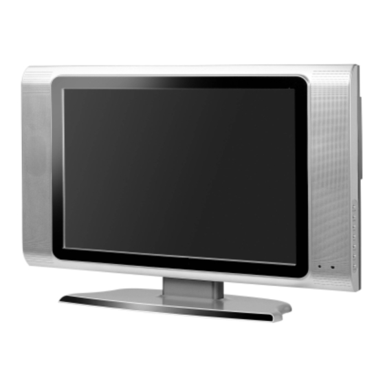
Summary of Contents for DiBoss LT-32HLFH
-
Page 1: Service Manual
COLOR TFT-LCD TV SERVICE MANUAL MODEL LT-32HLFH CAUTION !! BEFORE SERVICING THE TFT-LCD TV, READ THE SAFETY PRECAUTIONS IN THIS MANUAL. SERVICE MANUAL... -
Page 2: Table Of Contents
CONTENTS Contents ------------------------------------------------------------------------- 2 Safety precautions ----------------------------------------------------------- 3 Servicing precautions ------------------------------------------------------- 4 Specifications ------------------------------------------------------------------ 5 Location of control ----------------------------------------------------------- 9 Trouble Shooting ------------------------------------------------------------- 12 Deassembly procedure ---------------------------------------------------- 14 Exploded Drawing ----------------------------------------------------------- 19 Wire dressing ------------------------------------------------------------------ 21 Adjustment instruction with Default Factory Data----------------- 22 Inspection instruction ------------------------------------------------------ 24 PCB Layout --------------------------------------------------------------------- 28 Schematic Diagram -----------------------------------------------------------31... -
Page 3: Safety Precautions
SAFETY PRECAUTIONS !! Important Safety Notice !! Many electrical and mechanical parts in this chassis have special safety-related characteristics. These parts are identified by in the Schematic Diagram and Replacement Parts List. It is essential that these special safety parts should be replaced with the same components as recommended in this manual to prevent Shock, Fire, or other Hazards. -
Page 4: Servicing Precautions
SERVICING PRECAUTIONS CAUTION!! Before servicing receivers covered by this service manual, read and follow the SAFETY PRECAUTIONS on page 2 of this publication. General Servicing Precautions 1.Always unplug the receiver AC power cord from AC power source before; ¨ Í Removing or reinstalling any component, circuit board module or any other receiver assembly. ¨... -
Page 5: Specifications
SPECIFICATIONS Note: Specifications and others are subject to change without notice for improvement. 1.Scope. This document is the specification of 32” TFT-LCD Color TV. 2.Power 1) Power requirement 150W 2) AC / DC SMPS. Input Frequency : 50 / 60§ Ô Input Voltage: AC 100V- 240V 2.5A ~1.5A Output Voltage: DC 12V, 24V... - Page 6 SPECIFICATIONS 9.Receiving RF TV system LT-32HLFH Model System 1 PAL-B ¡ Û 2 PAL-G ¡ Û 3 PAL-I, I /I ¡ Û 4 PAL-D ¡ Û 5 PAL-K ¡ Û 6 SECAM-B ¡ Û 7 SECAM-G ¡ Û 8 SECAM-D ¡...
- Page 7 SPECIFICATIONS 10. PC Mode Scan Frequency & Timing 1) Scan Freq: H: 31¡ - 56 kHz / V: 56¡ - 75§ Ô 2) Preset Timing Chart Note!! : ¨ Í If the set is cold, there may be a small “flicker” when the set is switched on. This is Normal, there is nothing wrong with the set.
- Page 8 SPECIFICATIONS 11. TFT – LCD Panel Character Description LTA320W2-L03 is a color active matrix TFT(Thin Film Transistor) liquid crystal display(LCD) that uses amorphous silicon TFTs as a switching devices. This model is composed of a TFT LCD panel, a driver circuit and a back-light system. The resolution of a 32.0" contains 1366 X 768 pixels and can display up to 16.7 million colors with wide viewing anale of 85¢...
-
Page 9: Location Of Control
LOCATION OF CONTROL LOCATION OF CONTROL All the functions can be controlled with the remote controller. Some functions can also be adjusted with the buttons on the side panel of the set. Remote controller Before you use the remote controller, please install the batteries. 1. - Page 10 LOCATION OF CONTROL LOCATION OF CONTROL 14. PICTURE( Recalls your preferred picture setting 15. SOUND( Recalls your preferred sound setting 16. ARC( You can watch TV in various picture formats; Auto, 16:9, 14:9, 4:3, 16:9 Zoom, 14:9 Zoom, 4:3 Zoom. Repeatedly press the ARC button to select your desired picture format.
- Page 11 LOCATION OF CONTROL 1-3. Controller of Panel < SIDE VIEW> 1.ON/OFF: Switches TV set on or off. 2.MENU: Display a menu. ( Programme Up/Down): Selects a programme or a menu item. ( Volume Up/Down): Adjusts the volume. Adjusts menu settings. 5.TV/AV: Selects input signal source.
-
Page 12: Trouble Shooting
TROUBLE SHOOTING No Raster Check Check Replace LCD Panel. P803 (8~12) : 24V ? P303 (25~27) : 5V ? (If possible, re place P804 (6~10) : 24V inverter module.) Check Check Replace Q804 (3) : 24V ? IC805 (3) : 5V ? IC805 IC805 (4) : 0V ? - Page 13 TROUBLE SHOOTING No Sound & Picture OK IC601 (4,7,12,15) IC601 (25-Mute) ZD601 (C) IC202 (10) = 24V ? 0.7V ? < 1V? = 0V? < (L:Mute/ H:On) Check IC101 Replace Replace (123/124 L/R) 24V Line ZD601 IC202 Q104/105 (E) Sound Wave ? Replace IC101 No Operation LED blinking...
-
Page 14: Deassembly Procedure
DEASSEMBLY PROCEDURE 1. Disassembly procedure 1).Back cover Remove 4 screws Remove 16crews Removal of Backcover SERVICE MANUAL... - Page 15 DEASSEMBLY PROCEDURE 2).Metal plate & Rear chassis Remove 5 screws Removal of rear metal chassis... Remove 2 screws Slide away the metal plate SERVICE MANUAL...
- Page 16 DEASSEMBLY PROCEDURE 3).Metal plate & Rear chassis Remove Main PCB 10 screws Removal of Main PCB Remove 6 connector SERVICE MANUAL...
- Page 17 DEASSEMBLY PROCEDURE 4).LCD Panel chassis Remove 22 screws, then take LCD-BRKT Removal of LCD Module take LCD-BRKT Removal of LCD Module SERVICE MANUAL...
- Page 18 DEASSEMBLY PROCEDURE 5).LCD Module Remove 8 screws, then take LCD-BRKT Front mask remains after removing LCD Module SERVICE MANUAL...
-
Page 19: Exploded Drawing
MECHANICAL EXPLODED VIEW PART NO DESCRIP TION MATERKAL COLOR FINISH Q'TY DECO FRONT PMMA BLACK 610-006A SPEAKER 10W,10§Ù 400-021C FRONT COVER PC+ABS SILVER,BLACK 408-002D LENS SENSOR TRANSPARENCE IR PCB AYCOLT40A01A CONTROL PCB 404-004B BLOCK KNOB SILIVER 450-001Z CONTROL PLATE SILIVER PANV320W2L01 PANEL SAMSUNG... -
Page 20: Wire Dressing
WIRE DRESSING 1. Wire Dressing Note: Using acetate Using Copper (Conducted tape) Using Ferrite Cpre Using Copper Tape Using Conducted tape Using Ferrite Cpre SERVICE MANUAL... -
Page 21: Adjustment Instruction With Default Factory Data
ADJUSTMENT INSTRUCTION WITH DEFAULT FACTORY DATA 1.SVC mode data Adjustment NOTE!! When the EEPROM has been replaced, the SVC data should be restored as the function of individual system and specification. When the EEPROM has been replaced White Blance Checking. [ Enter and exit SVC mode ] Note: into the SVC mode, Initialize with default data. - Page 22 ADJUSTMENT INSTRUCTION WITH DEFAULT FACTORY DATA 2. White Blance Checking 5. Setting : All 1. Panel : SSLTA320W2-L03-10K 2. MODEL : L 3. Language Option : 4. PC Pattern Generator EU 14EA 1024 x 768, 60Hz (Pattern Generator : MSPG-3420) 6.
-
Page 23: Inspection Instruction
INSPECTION INSTRUCTION 1. Supplied Accessories Note: Make Sure the following accessories are provided with Product. SERVICE MANUAL... - Page 24 INSPECTION INSTRUCTION 2. Packing condition PACKING BOTTOM SET FRONT SET FRONT BOX FRONT <picture2> SET insert in BOX BOX FRONT <picture 1> PACKING insert in BOX PACKING TOP ACCESSORY BOX SET FRONT SET BACK SET FRONT <picture3> Accessory Box insert <picture4>...
- Page 25 PART NO DESCRIP TION MATERKAL COLOR Q'TY LCD COLOR TV 321-006A POLY VINLY 310-021A,B PACKING BOTTOM (L,R) WHITE 300-012B SET BOX PAPER ACCESSORY 310-022A,B PACKING TOP (L,R) WHITE 499-002A TAPE OPP TITLE MATERIAL DATA 2005. 10. 26 SET Packing Exploded Drawg THIS ENGR DRAWING NO.
-
Page 26: Pcb Layout
PCB LAYOUT 1. CONTROL PCB 2. Tuner PCB 3. SUB PCB SERVICE MANUAL... -
Page 32: Replacement Part List
TAPE, OPP 4000 499-004A W:20mm, L:30m TAPE, ACETATE 500-084D NO BRAND, ENG/TUR OWNERS MANUAL 501-001H WEEE LABEL, WARNING 501-003O COMMON LABEL,SERIAL 501-018G DIBOSS STICKER, LOGO 501-113E DIBOSS LABEL, ID 502-001O COMMON LABEL, BOX ID 509-009W DIBOSS LABEL, BRAND SERVICE MANUAL... - Page 33 REPLACEMENT PART LIST 2. Parts List (Assemble process) LEVEL PART NO PART NAME DESCRIPTION Q,TY 510-320A NO BRAND,(PR),symbol REMOCON (WEE),L-GRAY 520-001A 1.5V, AAA SIZE BATTERY 610-006A 10W,8Ohm(CT156B03K) SPEAKER 620-005D 32",SMPS,HNE,150W AD/DC ADAPTER 621-001B VDE KKP-4819R (EU) POWER CORD 626-002C IVORY,1.8M,15P,SHORT CABLE, PC RGB 627-001A 1.8M, BK...
- Page 34 REPLACEMENT PART LIST Description AYMALT52A01A LAVEL VENDOR P/N Description Q'ty Circuit No. 0JASCART001D JACK, SCART SCART/AV-6P J401,J403 GRLT51AA001B GR, SCART AUTO LAVEL VENDOR P/N Description Q'ty Circuit No. 0CESS100CMTR CESSL1C100M0511AD C240,C241 0CESS220CMTR CESSL1C220M0511AD 22U/16V C207,C208 GRLT51AS001B GR, SCART SMD LAVEL VENDOR P/N Description Q'ty...
- Page 35 REPLACEMENT PART LIST LAVEL VENDOR P/N Description Q'ty Circuit No. 2.2U 0CESS2R2HMTR Capacitor, 2.2UF 50V C178,C179,C187,C615,C619 3.3U 0CESS3R3HMTR Capacitor, 3.3UF 50V C165,C677 C121,C151,C185,C254,C514 0CESS470CMTR Capacitor, 47UF 16V C622,C671,C693,C697C844 0CESS471CMTR 470UF 16V 470U/16V C80,C802,C122 0CESS4R7HMTR Capacitor, 4.7UF 50V 4.7U/50V C106,C197 0.68U/50V 0CESS684HMTR Capacitor, 0.68UF 50V C823...
- Page 36 REPLACEMENT PART LIST LAVEL VENDOR P/N Description Q'ty Circuit No. 0ICVI4925DTS DUAL P-CHANNEL 30V MOSFET SI4925 IC805,IC821 L207,L208,L209L701,L702 0LBSS101DJTS 100 OHM, 2012 101/2012 L703,L502 L01,L03,L04,L05,L07 601/3216 0LBSS601FJTS 600 OHM, 3216 L08,L09,L104,L160,L23 L610,L501,L95,L603 L200,L201,L203,L204,L210 L211,L212,L213,L214,L215 12UH/2012 0LHSS120EJTS 12UH, 2012 L216,L217,L218,L220,L221 L222 33UH 0LRSL10100BS INDUCTOR...
- Page 37 REPLACEMENT PART LIST LAVEL VENDOR P/N Description Q'ty Circuit No. 0RHSS392DJTS Resistor, chip 3.9K 3.9K R124,R125 0RHSS393DJTS Resistor, chip 39K R619,R622 0RHSS3R0DJTS 3 OHM, 1608 J 0RHSS470DJTS Resistor, chip 47 ohm R257,R258 0RHSS471DJTS Resistor, chip 470 ohm R104,R275,R519 R119,R121,R122,R123,R177 R181,R182,R183,R184,R207 4.7K 0RHSS472DJTS Resistor, chip 4.7K...
- Page 38 REPLACEMENT PART LIST GRLT41AM001H GR, LL' MANUAL VCTI 15/17 µ¿ÀÏI LAVEL VENDOR P/N Description Q'ty Circuit No. 40.9M 1TPMU40R9MTD MKTGA40M9AAHP00A03 T101 GRLT41DS001G GR, LL' SMD V2327 ½Å±Ô LAVEL VENDOR P/N Description Q'ty Circuit No. 0TRKE3875STS KTC3875S C3875 Q106 4.7K 0RHSS472DJTS Resistor, chip 4.7K R177 GRLT51AS001G...
-
Page 39: Block Diagram
BLOCK DIAGRAM 1. Block Diagram 32 Block Diagram DC - I N DC - I N S P E A K E R P o w e r L C D P A N E L S O U N D A M P S C 2 L / R P r oce s s o r... -
Page 40: Circuit Descriptions
CIRCUIT DESCRIPTIONS General Description for 26.0” color TFT LCD TV. The TFT LCD TV described in the followings is based on a Multi TV system, digital Control display, 26.0" diagonal. The TFT LCD TV is intended to be a finished product, Basically a display device mounted inside an enclosure which will provide the safety Requirements. - Page 41 CIRCUIT DESCRIPTIONS 1.SCALER SECTION. Device : MST5151A Features: LCD TV controller with PC & multimedia display functions Input supports up to UXGA & 1080P Supports up to SXGA panels Integrated two-port triple-ADC/PLL Integrated DVI/HDCP/HDMI compliant receiver YUV422 digital video input ports Dual high-quality scaling engines Dual 3-D video de-interlacers Full function PIP/POP...
- Page 42 1) Description The MST5151A is a high performance and fully integrated graphics processing IC solution for multi-function LCD monitor/TV with resolutions up to SXGA. It is configured with an integrated triple-ADC/PLL, an integrated DVI/HDCP/HDMI receiver, two video de-interlacers, two high quality scaling engines, an on-screen display controller, and a built-in output clock generator.
- Page 43 CIRCUIT DESCRIPTIONS PIN DIAGRAM (MST5151A) VDDC DVI_G+ VDDM DVI_G- Pin 1 DQS[0] AVDD_DVI DVI_B+ MDATA[0] DVI_B- MDATA[1] MDATA[2] MDATA[3] DVI_CK+ DVI_CK- MDATA[4] AVDD_DVI MDATA[5] MDATA[6] REXT AVDD_PLL MDATA[7] MDATA[8] DDCD_DA MDATA[9] MDATA[10] DDCD_CK MDATA[11] AVDD_ADC HSYNC1 VDDM MDATA[12] VYSNC1 MDATA[13] BIN1P BIN1M MDATA[14]...
- Page 44 CIRCUIT DESCRIPTIONS PIN DESCRIPTION MCU Interface Pin Name Pin Type Function HWRESET Schmitt Trigger Input Hardware Reset, active high w/ 5V-tolerant DBUS[3:0] I/O w/ 5V-tolerant MCU 4-bit DDR Direct bus; 4mA driving strength 75-72 I w/ 5V-tolerant MCU Bus ALE, active high I w/ 5V-tolerant MCU Bus RDZ, active high I w/ 5V-tolerant...
- Page 45 CIRCUIT DESCRIPTIONS Pin Name Pin Type Function GIN1M Analog Input Reference Ground for Analog Green Input from Channel 1 RIN1P Analog Input Analog Red Input from Channel 1 RIN1M Analog Input Reference Ground for Analog Red Input from Channel 1 DVI Interface Pin Name Pin Type...
- Page 46 CIRCUIT DESCRIPTIONS LVDS Interface Pin Name Pin Type Function LVA0M Output A-Link Negative LVDS Differential Data Output LVA0P Output A-Link Positive LVDS Differential Data Output LVA1M Output A-Link Negative LVDS Differential Data Output LVA1P Output A-Link Positive LVDS Differential Data Output LVA2M Output A-Link Negative LVDS Differential Data Output...
- Page 47 CIRCUIT DESCRIPTIONS DRAM Interface Pin Name Pin Type Function MVREF Input Reference Voltage for DDR SDRAM Interface MCLKE Output DRAM Memory Clock Enable MCLKZ Output DRAM Memory clock Complementary /Input (for differential clocks) MCLK Output DRAM Memory Clock RASZ Output Row Address Strobe, active low CASZ Output...
- Page 48 CIRCUIT DESCRIPTIONS Pin Name Pin Type Function VDDM 3.3V Power (SDR SDRAM) / DRAM Interface Power 86, 102, 113, 125, 139, 2.5V Power (DDR SDRAM) VDDP 3.3V Power Digital Output Power 66, 162, 182 VDDC 1.8V Power Digital Core Power 63, 79, 131, 156, 173, 185, 195 Ground...
- Page 49 CIRCUIT DESCRIPTIONS MECHANICAL DIMENSIONS θ1 θ2 Gage Plane 0.25mm Seating Plane Millimeter Inch Millimeter Inch Symbol Symbol Min. Nom. Max. Min. Nom. Max. Min. Nom. Max. Min. Nom. Max. 4.10 0.161 θ 0° 7° 0° 7° θ1 0.25 0.010 0° 0°...
- Page 50 CIRCUIT DESCRIPTIONS General Description Features The VCT 49xxI family offers a rich feature set, cover- Introduction ing the whole range of state-of-the-art 50/60-Hz TV applications. The VCT 49xxI is an IC family of high-quality single- – PSSDIP88-1/-2 package chip TV processors. Modular design and deep-submi- cron technology allow the economic integration of fea- –...
- Page 51 CIRCUIT DESCRIPTIONS Chip Architecture IFIN+ Sound Audio Frontend Processor Demodulator Processor IFIN- PROT HOUT HFLB VERT Comb Color CVBS in Display & Filter Decoder YCrCb in Video Panorama Video Deflection Frontend Scaler Backend RGB in Processor Component RGB out CVBS out Interface RGB in SENSE...
- Page 52 CIRCUIT DESCRIPTIONS Pin Connections and Short Descriptions NC = not connected LV = if not used, leave vacant OBL = obligatory; connect as described in circuit diagram IN = Input Pin OUT = Output Pin SUPPLY = Supply Pin Pin No. Pin Name Type Connection...
- Page 53 CIRCUIT DESCRIPTIONS Pin No. Pin Name Type Connection Short Description PSSDIP PMQFP-2 (If not used) 88-pin 144-pin HFLB HOUT Horizontal Flyback Input HOUT Horizontal Drive Output VPROT Vertical Protection Input PWMV PWM Vertical Output DFVBL Dynamic Focus Vertical Blanking Output IN/OUT C Bus Data Input/Output IN/OUT...
- Page 54 CIRCUIT DESCRIPTIONS Pin No. Pin Name Type Connection Short Description PSSDIP PMQFP-2 (If not used) 88-pin 144-pin VIN10 Analog Video 10 Input VIN11 Analog Video 11 Input IN/OUT Port 2, Bit 3 Input/Output IN/OUT Port 2, Bit 2 Input/Output XTAL2 Analog Crystal Output XTAL1 Analog Crystal Input...
- Page 55 CIRCUIT DESCRIPTIONS Pin No. Pin Name Type Connection Short Description PSSDIP PMQFP-2 (If not used) 88-pin 144-pin SPEAKERL Analog Loudspeaker Output, Left VREFAU Reference Voltage, Audio VSUP8.0AU SUPPLY Supply Voltage Analog Audio, 8.0 V SUPPLY Ground Platform P37 / IN/OUT Port 3, Bit 7 Input/Output 656IO7 Digital 656 Bus 7 Input/Output...
- Page 56 CIRCUIT DESCRIPTIONS Pin No. Pin Name Type Connection Short Description PSSDIP PMQFP-2 (If not used) 88-pin 144-pin ADB10 Address Bus 10 Output ADB9 Address Bus 9 Output ADB8 Address Bus 8 Output ADB7 Address Bus 7 Output ADB6 Address Bus 6 Output ADB5 Address Bus 5 Output ADB4...
- Page 57 CIRCUIT DESCRIPTIONS CIRCUIT DESCRIPTIONS CIRCUIT DESCRIPTIONS CIRCUIT DESCRIPTIONS CIRCUIT DESCRIPTIONS Pin Descriptions than one capacitor. By choosing different values, the frequency range of active decoupling can be extended. Supply Pins VSUP1.8DIG − Supply Voltage 1.8 V IF Pins This pin is main and standby supply for the digital core VREFIF −...
-
Page 58: General Description
CIRCUIT DESCRIPTIONS General Description XREF − DAC Current Reference (Fig. 4–20) AOUT1 R/L – Audio 1 Outputs (Fig. 4–11) Output of the analog audio 1 signal. Connections to External reference resistor for DAC output currents, these pins are intended to be AC coupled. typical 10 kΩ... - Page 59 CIRCUIT DESCRIPTIONS General Description SENSE − Measurement ADC Input (Fig. 4–27) ADB0 − ADB19 − Address Bus Output (Fig. 4–35) This is the input of the analog to digital converter for These 20 lines provide the CPU address bus output to the picture and tube measurement.
- Page 60 CIRCUIT DESCRIPTIONS General Description IFIN+ P36 / 656IO6 P37 / 656IO7 IFIN- VREFIF VIN11 TAGC VIN10 VIN9 AIN1R / SIF AIN1L VIN8 VIN7 AIN2R VIN6 AIN2L VIN5 AIN3R VIN4 AIN3L VIN3 AOUT2R AOUT2L VIN2 AOUT1R VIN1 VOUT1 AOUT1L VOUT2 SPEAKERR VOUT3 SPEAKERL VSUP1.8FE...
- Page 61 CIRCUIT DESCRIPTIONS Advance Information Supplement Subject: Additional Info for VCT 49xyI Data Sheet Concerned: VCT 49xyI 6251-573-1AI, Edition Feb. 18, 2004 Supplement: Version History Edition: Dec. 16, 2004 Changes to the previous revision are indicated by change bars. Please note section 2.1.1.2., which is of importance for the use of the VCT-I F1 in combination with NICAM-audio modes.
- Page 62 CIRCUIT DESCRIPTIONS Table 1–2: History of functional problems, continued Functional Problem Comment Peaking Filter Problem solved in D2 Bandwidth of Antialias Filter Problem solved in D2 SVM Overflow Problem solved in D2 ADC Initialisation Problem solved in D2 a) Clock Noise ! = Applicative methods solve the problem to a large extent...
- Page 63 CIRCUIT DESCRIPTIONS Table 1–2: History of functional problems, continued Functional Problem Comment ODC-Modes: FHPULLIN/ ! = Workaround available SHPULLIN no redesign planned Safety Pin Problem solved in F1 13.5MHz Backend Mode - = new feature in D2, Problem solved in F1 ITU656 Interference - = new feature in D2, Problem solved in F1...
- Page 64 CIRCUIT DESCRIPTIONS 7. VCT 49xyI-C7 The VCT 49xyI-C7 is pin-compatible to VCT 49xyI-C6 and VCT 49xyI-C4. Problem 45 has been solved. Problem 43 is partly solved: Improved internal clock suppression leads to reduced noise floor and better video snr. Problems 53 and 54 have not been detected before D2. VCT 49xyI-C7 includes functionality of DRX396xA-H8.
- Page 65 CIRCUIT DESCRIPTIONS Problem Description Comment DRX AGC Hangup If VAGC_REDUC>0 and positive firmware redesign D1 signal jumps above top level, AGC workaround: hangup may occur and CVBS out- put level is reduced. KI_CHANGE_TH = 19 after stan- dard change MSP Automatic Stan- Automatic standard detection fails, firmware redesign D4 dard Detection...
- Page 66 CIRCUIT DESCRIPTIONS 2. VCT 49xyI-F1 The VCT 49xyI-F1 is targeted to solve field and functional problems of the earlier VCT-I versions. For that purpose some new registers were implemented. In addition workarounds used for VCT-I versions prior to F1 may not be compatible.
- Page 67 CIRCUIT DESCRIPTIONS 2.1. Register Changes on VCT 49xyI-F1 2.1.1. DRX Part The major improvement of the VCT 49xyI-F1 DRX-performance is based on the speed up of the Tuner-AGC, the Video AGC and the Carrier Recovery. While the faster Tuner and Video AGC help to improve significantly the Streaky Noise and Airplane Flutter issues, the extended Carrier Recovery removes all remaining field test matters.
- Page 68 CIRCUIT DESCRIPTIONS All controller software workarounds used at former versions which write the KIs will no longer be needed and should be removed (see also next section). 2.1.1.2. Comments to the Carrier Recovery in Connection with NICAM Audio Performance The speed up of the carrier recovery to optimize the performance at non standard RF signals (caused by FM modu- lation and modulator imbalance) is mainly based on a significant extension of the PLL-bandwith.
- Page 69 CIRCUIT DESCRIPTIONS Problem Countries Workaround Side-Effect Status in F1 Recommen- for C7 / Dx dation for F1 Hsync Distortion Malaysia Speed up DRX video AGC: none previously remove WA forced val- - KI_CHANGE_TH=1 ues now default - VAGC_REDUC=1 Color Sensitivity, India, Reduce NOISE_BS to 8 Measured...
- Page 70 CIRCUIT DESCRIPTIONS 2.1.2. VSP Part Table 2–5: New VSP Registers Name Sync Reset Range Function LPCDEL[2:0] h07[2:0] VS_CD -8..7 Window Shift For Fine Error Calculation 100: -4 clock cycles 000: no offset 011: +3 clock cycles THRSEL[1:0] h07[13:12] VS_CD 0,1,2,3 H Slicing Level Threshold 00: 50% 01: 31%...
- Page 71 CIRCUIT DESCRIPTIONS Table 2–5: New VSP Registers, continued Name Sync Reset Range Function COMB h1F[4] VS_CO Vertical Peaking Mode 0: 2H PAL, 1H NTSC (old mode) 1: 1H PAL, 2H NTSC (new mode) MACROVISION MVRESULT[1:0] h26[1:0] VS_CD 0,1, 2, 3 Macrovision Detection 00: nothing present 01: AGC process present and colorstripe process not...
- Page 72 CIRCUIT DESCRIPTIONS 2.1.3. DPS Part Table 2–9: New DPS Registers Name Sync Reset Range Function DEFL FBOUTEN hD3[0] VS_DEFL FBOUT Enable at PWMV pin 0: PWMV to Port Mux 1: FBOUT to Port Mux Table 2–10: Undocumented DPS Registers (already available in Dx versions) Name Sync Reset...
- Page 73 CIRCUIT DESCRIPTIONS Table 2–12: Undocumented XDFP Registers (already available in Dx versions) Name Sync Reset Range Function Horizontal Deflection PER_MIN[10:0] h0183[10:0] 1140 0..2047 HSync Period Minimum PER_MAX[10:0] h0184[10:0] 1426 0..2047 HSync Period Maximum 2.1.5. TVT Part Table 2–13: Wrongly Documented TVT Registers Name Addr Reset...
Need help?
Do you have a question about the LT-32HLFH and is the answer not in the manual?
Questions and answers