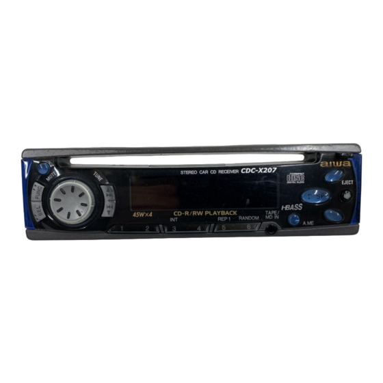
Aiwa CDC-X207 Service Manual
Stereo car cd receiver
Hide thumbs
Also See for CDC-X207:
- Operating instructions manual (18 pages) ,
- Installation and connections (4 pages) ,
- Service manual (11 pages)
Table of Contents
Advertisement
SERVICE MANUAL
STEREO CAR CD RECEIVER
• This Service Manual is the "Revision Publishing" and replaces "Simple Manual"
of CDC-X207/ X307/ X407<YU>, (S/M Code No. 09-99B-422-3T1) and
CDC-X2070/ X3070/ X4010<YL>, (S/M Code No. 09-99C-422-3T2).
CDC-X207
CDC-X307
CDC-X407
CDC-X2070
CDC-X3070
CDC-X4010
BASIC CD MECHANISM: TN-CCD1001-113J
S/M Code No. 09-002-422-3R1
YU
YU
YU
YL
YL
YL
Advertisement
Table of Contents

Subscribe to Our Youtube Channel
Related Manuals for Aiwa CDC-X207


Summary of Contents for Aiwa CDC-X207
- Page 1 STEREO CAR CD RECEIVER BASIC CD MECHANISM: TN-CCD1001-113J • This Service Manual is the “Revision Publishing” and replaces “Simple Manual” of CDC-X207/ X307/ X407<YU>, (S/M Code No. 09-99B-422-3T1) and CDC-X2070/ X3070/ X4010<YL>, (S/M Code No. 09-99C-422-3T2). S/M Code No. 09-002-422-3R1...
-
Page 2: Specifications
SPECIFICATIONS RADIO SECTION AUDIO SECTION (FM) Max. Power Output 45 W x 4 channels Frequency Range 87.5 MHz –108 MHz (100-kHz steps) <except CDC-X2070> 87.5 MHz –108 MHz (50-kHz steps) 35 W x 4 channels <CDC-X2070 only> Usable Sensitivity 12.7 dBf 50 dB Quieting Sensitivity 17.2 dBf TAPE/MD IN input IF Rejection... -
Page 3: Protection Of Eyes From Laser Beam During Servicing
PROTECTION OF EYES FROM LASER BEAM DURING SERVICING CAUTION This set employs laser. Therefore, be sure to follow carefully the instructions below when servicing. Use of controls or adjustments or performance of proce- dures other than those specified herin may result in WARNING!! hazardous radiation exposure. - Page 4 ELETRICAL MAIN PARTS LIST REF. NO. PART NO. KANRI DESCRIPTION REF. NO. PART NO. KANRI DESCRIPTION C205 87-A11-606-080 C-CAP,S 0.22-25 K B C206 87-010-492-040 CAP,E 0.33-50 GAS 87-A20-446-010 C-IC,LA9241ML C207 87-010-195-080 C-CAP,S 0.068-25 Z F C2012 87-A21-319-010 C-IC,LC78622NE C208 87-010-176-080 C-CAP,S 680P-50 J SL 87-A21-488-040 C-IC,LA6556...
- Page 5 REF. NO. PART NO. KANRI DESCRIPTION REF. NO. PART NO. KANRI DESCRIPTION C311 87-A11-177-080 C-CAP,S 0.15-16 K B C832 87-010-494-040 CAP,E 1-50 M 5L SRE C312 87-A11-177-080 C-CAP,S 0.15-16 K B C835 87-010-182-080 C-CAP,S 2200P-50 K B C2012 C313 87-A11-177-080 C-CAP,S 0.15-16 K B C836 87-010-182-080...
-
Page 6: Chip Resistor Part Code
CHIP RESISTOR PART CODE Chip Resistor Part Coding Figure Resistor Code Value of resistor Chip resistor Dimensions (mm) Wattage Type Tolerance Symbol Resistor Code Form 1/16W 1005 0.35 1/16W 1608 0.45 1/10W 2125 1.25 0.45 1/8W 3216 0.55 TRANSISTOR ILLUSTRATION E C B E C B B C E... - Page 7 WIRING - 1 (YU: MAIN) 1 / 2...
- Page 8 WIRING - 1 (YU: MAIN) 2 / 2...
- Page 9 SCHEMATIC DIAGRAM - 1 (YU: MAIN 1 / 2)
- Page 10 SCHEMATIC DIAGRAM - 2 (YU: MAIN 2 / 2) -10-...
- Page 11 WIRING - 2 (YL: MAIN) 1 / 2 -11-...
- Page 12 WIRING - 2 (YL: MAIN) 1 / 2 -12-...
- Page 13 SCHEMATIC DIAGRAM - 3 (YL: MAIN 1 / 2) -13-...
- Page 14 SCHEMATIC DIAGRAM - 4 (YL: MAIN 2 / 2) -14-...
-
Page 15: Wiring - 3 (Front)
WIRING - 3 (FRONT) -15-... -
Page 16: Schematic Diagram - 5(Front)
SCHEMATIC DIAGRAM - 5(FRONT) -16-... -
Page 17: Ic Block Diagram
IC BLOCK DIAGRAM IC,LA4743B IC,LA6556 -17-... - Page 18 VOLTAGE CHART IC, LC72358N-9910 PIN NO. BU (V) BU+ACC (V) FM (V) AM(V) CD (V) AUX (V) PIN NO. BU (V) BU+ACC (V) FM (V) AM(V) CD (V) AUX (V) 2.45 2.47 2.35 2.35 2.42 2.28 4.94 4.95 4.76 4.76 4.87 4.79 2 ~ 6...
- Page 19 IC, LA9241ML PIN NO. BU (V) BU+ACC (V) FM (V) AM(V) CD (V) AUX (V) PIN NO. BU (V) BU+ACC (V) FM (V) AM(V) CD (V) AUX (V) 1 ~ 2 2.50 2.53 2.22 3.71 2.49 0.19 5 ~ 7 2.51 2.52 4.91...
- Page 20 IC, LC78622NE PIN NO. BU (V) BU+ACC (V) FM (V) AM(V) CD (V) AUX (V) PIN NO. BU (V) BU+ACC (V) FM (V) AM(V) CD (V) AUX (V) 0.05 1.93 2.34 1.55 62 ~ 64 1.77 4.69 0.33 TU UNIT, FAE347-A12 2.49 2.39 PIN NO.
- Page 21 IC, LC75374E IC, LC75853NW PIN NO. BU (V) BU+ACC (V) FM (V) AM(V) CD (V) AUX (V) PIN NO. BU (V) BU+ACC (V) FM (V) AM(V) CD (V) AUX (V) 3.94 3.93 3.96 3.96 4.84 4.83 4.86 4.85 3.98 3.98 4.00 4.01 4.00...
- Page 22 IC DESCRIPTION IC, LC72358N-9910 Pin No. Pin Name Description Pin No. Pin Name Description System clock oscillator input. Read / write control output terminal. 2 ~ 3 Not connected. CD RES DSP reset output terminal. E-VOL DO Data output for electric volume. Disc detection / chuck or release disc detection.
- Page 23 IC, LA9241ML Pin No. Pin Name Description Pin No. Pin Name Description The HFL (high frequency level) signal is used to judge whether the main beam is For the connection of the pickup photodiode. Addition to the FIN1 pin creates an RF FIN2 positioned on the pit or on the mirror.
- Page 24 IC, LC78622NE Pin No. Pin Name Description Pin No. Pin Name Description DEFI Defect detection signal (DEF) input. (Must be connected to 0V when unused.) RVSS Right channel ground. (Must be connected to 0V.) For PLL/Test input. A pull-down resistor is built-in. (Must be connected to 0V.) RCHO Right channel output.
- Page 25 IC, LC75374E Pin No. Pin Name Description Pin No. Pin Name Description RVRIN 4dB volume control input. Must be driven at a low impedance. TP(R) RCOM – 1dB volume control common pin. TUN(R) Signal input pins. CD(R) For the connection of capacitors that compensate for bass and treble in the tone control AUX(R) circuits.
-
Page 26: Lcd Diagram
LCD DIAGRAM -26-... -
Page 27: Cd Test Mode
CD TEST MODE Caution when servicing 1-1 How to Activate CD Test Mode (1) How to use extension jig. 1) Connect 62 pin (test) of IC701 (LC72358N-9910) on Correct between MAIN C.B. and CD mechanisms by extension jigs when checking CD mechanism MAIN C.B to the 31 pin (VDD) by cable. -
Page 28: Mechanical Exploded View
MECHANICAL EXPLODED VIEW 1 / 1 P.C.B PANEL, HT-SINK TN-CCD1001-113J P.C.B HT-SINK P.C.B -28-... -
Page 29: Mechanical Parts List
MECHANICAL PARTS LIST 1 / 1 REF. NO. PART NO. KANRI DESCRIPTION REF. NO. PART NO. KANRI DESCRIPTION 1 8A-KC7-005-010 KNOB,RTRY -AC 30 8A-KCF-020-010 CABI,TRIM -AC15 2 8A-KC7-020-010 RING,RTRY -AC 31 8Z-KC2-203-210 LEVER,DFP HOOK -C2 3 8A-KC7-220-010 SPR-C,ROTARY -AC 32 8Z-KC2-221-110 SPR-C,DETACH HOOK-C2 4 8A-KCG-004-010 WINDOW,LCD X207<207>... -
Page 30: Cd Mechanism Exploded View
CD MECHANISM EXPLODED VIEW 1 / 1 20 19 P.C.B -30-... -
Page 31: Cd Mechanism Parts List
CD MECHANISM PARTS LIST 1 / 1 REF. NO. PART NO. KANRI DESCRIPTION REF. NO. PART NO. KANRI DESCRIPTION 1 S3-031-010-010 FRAME 2 S3-031-050-240 DAMPER(J) 41 S3-031-050-220 LOCK PIN BL 3 S3-031-010-260 REAR OAMPER BKT(J) 42 S3-031-050-080 PU SHAFT 4 S3-031-010-270 FPC GUIDE 43 S6-901-160-110 PICK-UP OPTIMA-720AIE... - Page 32 2–11, IKENOHATA 1–CHOME, TAITO-KU, TOKYO 110, JAPAN TEL:03 (3827) 3111 9820572 0251431 Printed in Singapore...
Need help?
Do you have a question about the CDC-X207 and is the answer not in the manual?
Questions and answers