
Related Manuals for Velleman K4005B


Summary of Contents for Velleman K4005B
- Page 1 400W MONO/STEREO AMPLIFIER Total solder points: 264 Difficulty level: beginner 1 4 ⌧ 5 advanced K4005B K4005B ILLUSTRATED ASSEMBLY MANUAL H4005B-IP-2...
-
Page 2: Specifications
Features & specifications Features: Rms output power : 2 x 100W / 4ohm ; 2 x 75W / 8ohm. Rms mono-bridged power : 200W / 8ohm. Total music output : 400W. Harmonic distortion : 0.003% at 1KHz. Signal-to-noise ratio : 96dB (A-weighted). Stereo channel separation : 76dB. - Page 3 Assembly hints 1. Assembly (Skipping this can lead to troubles ! ) Ok, so we have your attention. These hints will help you to make this project successful. Read them carefully. 1.1 Make sure you have the right tools: • A good quality soldering iron (25-40W) with a small tip.
- Page 4 Assembly hints 1.3 Soldering Hints : 1- Mount the component against the PCB surface and carefully solder the leads 2- Make sure the solder joints are cone-shaped and shiny 3- Trim excess leads as close as possible to the solder joint REMOVE THEM FROM THE TAPE ONE AT A TIME ! DO NOT BLINDLY FOLLOW THE ORDER OF THE COMPONENTS ONTO THE TAPE.
- Page 5 Construction 1. Jumpers J : 8X Choice between different input sensitivities : Mount the jumpers JH for a sensitivity of 950mV. Mount the jumpers JM for a sensitivity of 500mV. Leave both jumper connections OPEN for a sensitivity of 150mV. A bipolair THREE POSITION switch may be mounted here as well! Choice between stereo or mono : Mount the jumpers JS for a stereo amplifier.
-
Page 6: Ceramic Capacitors
Construction R14 : 68K (6 - 8 - 3 - B) 8. IC sockets. R15 : 220K (2 - 2 - 4 - B) R16 : 1K5 (1 - 5 - 2 - B) R17 : 1K5 (1 - 5 - 2 - B) R18 : 560 (5 - 6 - 1 - B) R19 : 560... -
Page 7: Spade Connectors
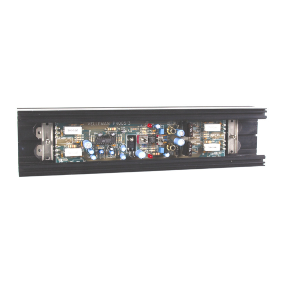
Assembly 11. Fuse holders + Fuses 15. Led’s. Watch the polarity! LD1 : 5mm red. F... LD2 : 5mm red. LD... 20mm F1 : 6,3A “slow” CATHODE F2 : 6,3A “slow” 16. Cinch connector(s) 12. Capacitors C... C21 : 1µF/63V For stereo use : C22 : 1µF/63V Left input... - Page 8 PCB mounting 18. Mount the PCB in the heat sink Slide the PCB in the largest slot of the heat sink. (See fig. 1.0) FIG. 1.0 Note : If the optional thermal protection is used, a hexagonal bolt should be slit into the mounting slot, and into the hole in the P.C.B.
- Page 9 Power transistors 19. Power transistors Two transistors are mounted at both ends of the heat sink (for their positions refer to Fig. 3.0). T1 & T2 : TIP142 of motorola! T3 & T4 : TIP147 of motorola! FIG. 3.0 Bend the connections of each transistor as in Fig. 4.0. FIG.
- Page 10 Power transistors Apply a drop of paste on each transistor and put them in the correct position on the heat sink and against the P.C.B. Make sure the correct type of transistor is placed in the correct position (T1...T4). Fix the transistors well in place by means of the supplied plate and a hexagonal bolt, which is slit into the slot in the heat sink (see Fig.
- Page 11 Test & Use 20. Test Connect a symetrical power supply unit (possibly the APS200, SPS200 or K3508 module) of + and - 30 tot 45VDC to the positions GND (0V), -V and +V. See Fig. 7.0. FIG. 7.0 IMPORTANT: Do not switch on the supply voltage before the connections to the amplifier are made! Switch on the supply voltage.
- Page 12 Use & connections 2. As a mono-bridged amplifier: • See Fig. 9.0 for the connection of the power supply and the speaker. • Make sure that the impedance of the connected speaker is not less than 8 ohms. FIG. 9.0 IMPORTANT: Always connect the outputs first, before the power supply is switched on.
- Page 13 Diagram 22. Diagram power supply...
- Page 14 23. PCB...
- Page 15 VELLEMAN NV Legen Heirweg 33 9890 Gavere Belgium Europe www.velleman.be www.velleman-kit.com...
- Page 16 VELLEMAN KIT NV Legen Heirweg 33 9890 Gavere Belgium Europe Info ?: http://www.velleman.be Modifications and typographical errors reserved © Velleman Kit nv H4005B_IP - 2004 - ED2 (rev2) 5 4 1 0 3 2 9 2 9 1 8 9 1...
Need help?
Do you have a question about the K4005B and is the answer not in the manual?
Questions and answers