Table of Contents
Advertisement
Quick Links
See also:
Owner's Manual
This document is printed on chlorine free (ECF) paper with soy ink.
GA
011540
20001101-75000
GUITAR AMPLIFIER
SERVICE MANUAL
CONTENTS
SPECIFICATIONS
PANEL LAYOUT
CIRCUIT BOARD LAYOUT
BLOCK DIAGRAM
WIRING
................................................................... 10
DISASSEMBLY PROCEDURE
LSI PIN DESCRIPTION
IC BLOCK DIAGRAM
CIRCUIT BOARDS
TEST PROGRAM
ERROR MESSAGES
IDLING ADJUSTMENT
MIDI IMPLEMENTATION CHART ......................................... 34
PARTS LIST
OVERALL CIRCUIT DIAGRAM
................................................ 3/4
.................................... 5
................. 7
............................ 8
............................ 11
.............................. 15
................................... 18
........................................ 20
................................. 30
............................. 33
........................ 33
HAMAMATSU, JAPAN
1.552K-448 I.T
Printed in Japan 2000.11
DG60FX-112
1
Advertisement
Table of Contents

Related Manuals for Yamaha DG60FX-112


Summary of Contents for Yamaha DG60FX-112
- Page 1 DG60FX-112 GUITAR AMPLIFIER SERVICE MANUAL CONTENTS SPECIFICATIONS ..........3/4 PANEL LAYOUT ........5 CIRCUIT BOARD LAYOUT ....7 BLOCK DIAGRAM ......8 WIRING ..............10 DISASSEMBLY PROCEDURE ......11 LSI PIN DESCRIPTION ......15 IC BLOCK DIAGRAM ........18 CIRCUIT BOARDS ........
-
Page 2: Dg60Fx
IMPOR TANT NOTICE This manual has been provided for the use of authorized Yamaha Retailers and their service personnel. It has been assumed that basic service procedures inherent to the industry, and more specifically Yamaha Products, are already known and under- stood by the users, and have therefore not been restated. -
Page 3: Specifications
DG60FX-112 SPECIFICATIONS Digital Section A/D Converter • Full Digital Signal Processing 20 bit + 3 bit Floating • 8 Channel Preamp D/A Converter • Digital Effects • Compressor 20 bit • Chorus, Flanger, Phaser, Rotary Speaker, Tremolo Sampling Frequency • Digital Delay, Tape Echo •... - Page 4 DG60FX-112...
-
Page 5: Panel Layout
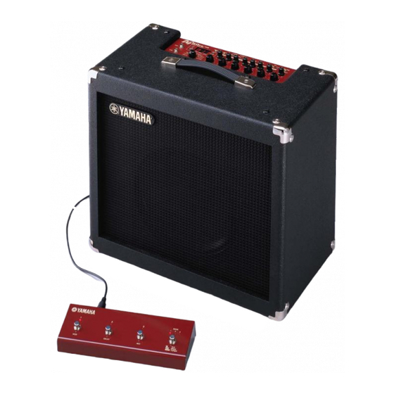
DG60FX-112 PANEL LAYOUT Control Panel 11 12 Input Jacks (INPUT HIGH, LOW) Peak Indicator Amp Select Switch (LEAD1-CLEAN2) Gain Control (GAIN) Master Volume (MASTER) Tone Controls (TREBLE, MIDDLE, BASS, PRESENCE) Output Level Control (OUTPUT) Speaker Simulator Button (SP. SIM) Up Button (UP) - Page 6 DG60FX-112 Rear Panel Power Switch (POWER) Headphones Jack (PHONES) Line Out Jacks (LINE OUT R, L/MONO) POWER AMP IN Jack Foot Switch Unit Terminal (FOOT SW) MIDI OUT Jack MIDI IN Jack Digital Out Jack (DIGITAL OUT) Foot Switch Unit...
-
Page 7: Circuit Board Layout
DG60FX-112 CIRCUIT BOARD LAYOUT MAIN MAIN MAIN MAIN MAIN FRONT (PN1/2) MAIN MAIN Foot Switch REAR (ANALOG8/8) SW, LED (PN2/2) -
Page 8: Block Diagram
DG60FX-112 BLOCK DIAGRAM MAIN FRONT CN101 IC401 IC402 IC102 IC102 CN103 IC103 IC103 W401 IC401 CN102 CN103 IC104 IC2 , IC3 IC10 , IC11 IC12 ( DM-CN1 ) ( DM-CN2 ) ( FRONT-CN303 ) FRONT (PN1/2) ( FRONT-CN304 ) - Page 9 DG60FX-112 MAIN (1/8, 2/8, 4/8~7/8) FRONT IC501 W502 IC501 CN102 CN103 IC502 IC502 C10 , IC11 ( DM-CN3 ) ( FRONT-CN302 ) REAR W701 SW, LED CN306 KEC-54207...
-
Page 10: Wiring
DG60FX-112 WIRING MAIN MAIN MAIN MAIN W602 W609 W607 W605 POWER SPEAKER TRANSFORMER CN603 CN607 W608 W606 CN102 W604 CN103 CN602 MAIN CN104 CN101 W603 W601 CN601 W611 W612 W610 W502 W501 W503 MAIN CN304 CN303 CN302 CN305 CN401 W401... -
Page 11: Disassembly Procedure
DG60FX-112 DISASSEMBLY PROCEDURE External components Handle Assembly 1-1. Remove the two (2) screws marked [70]. The handle assembly can then be removed. (Fig. 1) Corner fitting 2-1. Remove the two (2) screws marked [50]. The corner fitting can then be removed. (Fig. 1) 3-1. - Page 12 DG60FX-112 4. Removal of stereo amplifier unit 4-1. Remove the four (4) screws marked [80] and the four (4) washers marked [90] from the back plate and then remove the back plate. (Fig. 2) 4-2. Remove the six (6) screws marked [30] and the six (6) washers marked [40] from the top of the main unit.
- Page 13 DG60FX-112 MAIN MAIN MAIN MAIN MAIN [290] [290] [310] [290] [210] [50] MAIN [220] FRONT (PN1/2) [110] [110] [50]: Bind Head Tapping Screw-B 3.0X8 MFZN2BL (EP600190) [110]: Bind Head Tapping Screw-C A4.0X8 MFZN2BL (VC688900) [210]: Hexagonal Nut 9.0 12X2 MFNI33 (LX200060) [220]: Flat Washer 9X14 0.5 FNM3 (VL802300)
- Page 14 DG60FX-112 Power transformer 8-1. Remove the pre main unit. (See Procedure 4.) 8-2. Remove the panel. (See Step 6-2.) 8-3. Remove the four (4) screws marked [110B]. The transformer can then be removed. (Fig. 4) [110B] [110A] [130] [110A] [130] [110A] [130] [110A] [130]...
- Page 15 DG60FX-112 Foot switch Foot switch 9-1. Remove the six (6) screws marked [110A] and then remove the bottom plate. (Fig. 5) 9-2. Remove the two (2) screws marked [110B] and hexagonal nuts marked [90] and then remove the REAR circuit board (MAIN 8/8). (Fig. 5) 9-3.
-
Page 16: Lsi Pin Description
DG60FX-112 LSI PIN DESCRIPTION HD6413002FP16 (XQ375A00) CPU <H8/3002> DM: IC12 NAME FUNCTION NAME FUNCTION Port A Address bus Power supply Address bus Port B Ground P60//WAIT PB6//DREQ0 P61//BREQ Port 6 PB7//DREQ1 /RESO Reset P62//BACK Ground Ø Øout P90/TXD0 Transmit data (MIDI OUT) - Page 17 DG60FX-112 YSS910-S (XV988A00) DSP6 (Digital Signal Processor) DM: IC8, IC9 NAME FUNCTION NAME FUNCTION Power supply (3.3 V) Ground Ground DB13 System master clock input (60 MHz or 30 MHz) DB14 System master clock output (High or 30 MHz) DB15...
-
Page 18: Ic Block Diagram
DG60FX-112 AK4520A-VF-E2 (XT802A00) DAC & ADC DM: IC104 NAME FUNCTION NAME FUNCTION VREFH Positive Voltage Reference Input, VA MCLK Master Clock Input VREFL Negative Voltage Reference Input, AGND DEM0 De-emphasis Frequency Select AINR+ Rch Analog Positive Input DEM1 De-emphasis Frequency Select... - Page 19 DG60FX-112 NJM5532M (XC011A00) NE5532P (IG102500) NJM4556AD (XQ824A00) DM: IC102, IC103, IC106 DM: IC502 MAIN: IC501 OP AMP OP AMP OP AMP NJM4556AMT1 (XQ138A00) DM: IC105 OP AMP +DC Voltage +DC Voltage Output A Output A +V 8 Supply Supply Inverting...
-
Page 20: Circuit Boards
DG60FX-112 CIRCUIT BOARDS DM Circuit Board CN101: to MAIN3/8-W401 CN103: to PN1/2-CN301 CN102: to MAIN2/8-W502 to PN Battery VN103500 VN103600(Battery holder for VN103500) • Notice for back-up battery removal Push the battery as shows in figure, then the battery will pop up. - Page 21 DG60FX-112 CN104: to MAIN1/8-W601 to PN1/2-CN302 to PN1/2-CN303 to PN1/2-CN304 to MAIN1/8-W603 Component side DM: CNA-V620530...
- Page 22 DG60FX-112 DM Circuit Board...
- Page 23 DG60FX-112 Pattern side...
- Page 24 DG60FX-112 FRONT (PN1/2) to MAIN2/8-W503 to DM-CN3 SW, LED (PN2/2) LD302, LD303, LD304 and LD306 installation Anode PN: CNA-V620230...
- Page 25 DG60FX-112 to DM-CN103 to DM-CN2 to DM-CN1 Component side Component side...
- Page 26 DG60FX-112 FRONT (PN1/2) SW, LED (PN2/2) to Push Switch to Push Switch...
- Page 27 DG60FX-112 Pattern side to MAIN8/8-W701 to Push Switch to Push Switch Pattern side PN: CNA-V620230...
- Page 28 DG60FX-112 MAIN (ANALOG)1/8 Circuit Board to POWER TRANSFORMER W608: to MAIN 7/8-W609 CN607: N.C W606: to MAIN6/8-W607 to POWER W604: TRANSFORMER to MAIN5/8-W605 W601: to MAIN4/8-W602 W603: to POWER CORD to DM-CN4 W610: to DM-CN104 W611: to MAIN3/8-CN401 W612: to MAIN2/8-W501...
- Page 29 DG60FX-112 MAIN (ANALOG)2/8 Circuit Board to MAIN1/8-W612 to DM-CN102 to PN1/2-CN305 Component side MAIN (ANALOG)4/8 MAIN (ANALOG)5/8 MAIN (ANALOG)3/8 Circuit Board Circuit Board Circuit Board to MIAN1/8-W601 to MIAN1/8-W604 Component side Component side MAIN (ANALOG)6/8 MAIN (ANALOG)7/8 Circuit Board Circuit Board...
-
Page 30: Test Program
DG60FX-112 TEST PROGRAM A. PREPARATION • EXP. PEDAL Connect the B50KVR. • DIGITAL OUT Connect the DA converter. • MIDI IN Connect IN and OUT, using the DIN • MIDI IN 5P cable. • The input signal is a 1kHz sine wave. - Page 31 DG60FX-112 VR Check • Using the UP and DOWN switches, select “2” and then press the STORE switch. • Press switches in the order of “AMP SELECT”, “GAIN” until “PRESENCE, then from “COMP” to “REVERB” and finally until “EXP.PEDAL” is reached.
- Page 32 DG60FX-112 6: DSP Electric Characteristic • Using the UP and DOWN switches, select “6” and then press the STORE switch. The same output level is obtained when No. at the right end is “0” and when it is “1”. • To check the output level, noise level and distortion factor, enter the signal to be measured (short the input with GND for the noise level check).
-
Page 33: Error Messages
SOLUTION: Continued use of the device will result in the loss of data. Return the device to the music dealer where you purchased it or, the nearest Yamaha Service center and have the battery replaced. IDLING ADJUSTMENT 1. Tu r n t h e i d l i n g a d j u s t m e n t vo l u m e ( V R 6 0 1 ) counterclockwise fully. -
Page 34: Midi Implementation Chart
DG60FX-112 YAMAHA [ Guitar Amplifier] Date:30-Jun-2000 Model DG60FX-112 MIDI Implementation Chart Version : 1.0 +----------------------------------------------------------------------+ Transmitted Recognized Remarks Function ... : :-------------------+----------------+----------------+----------------: :Basic Default : 1 - 16 : 1 - 16, off : memorized :Channel Changed : 1 - 16... -
Page 35: Parts List
GUITAR AMPLIFIER PARTS LIST CONTENTS OVERALL ASSEMBLY ..........2 PRE MAIN UNIT ........4 FOOT SWITCH ..........6 ELECTRICAL PARTS ..........7 Notes : DESTINATION ABBREVIATIONS A : Australian model M : South African model B : British model O : Chinese model C : Canadian model Q : South-east Asia model D : German model... - Page 36 DG60FX-112 OVERALL ASSEMBLY Pre main unit (See page4) G120 G100 G110...
- Page 37 DG60FX-112 PART NO. DESCRIPTION REMARKS REF NO. RANK OVERALL ASSEMBLY DG60FX Overall Assembly (V632160) Overall Assembly C, U (V632170) Overall Assembly (V632180) Overall Assembly B, S (V632190) Pre Main Unit (V632220) Pre Main Unit C, U (V632230) Pre Main Unit...
- Page 38 DG60FX-112 PRE MAIN UNIT 20 (1) 20 (2)
- Page 39 DG60FX-112 PART NO. DESCRIPTION REMARKS REF NO. RANK Pre Main Unit (V632220) Pre Main Unit C, U (V632230) Pre Main Unit (V632240) Pre Main Unit B, S (V632250) V 6 1 2 5 4 0 0 Chassis V 6 1 2 5 5 0 0...
- Page 40 DG60FX-112 FOOT SWITCH OVERALL ASSEMBLY PART NO. DESCRIPTION REMARKS REF NO. RANK Foot SW Overall Assembly J, U (V632200) Foot SW Overall Assembly (V632210) V 6 1 4 5 8 0 0 SW Top Cover V 6 3 3 7 6 0 0...
-
Page 41: Electrical Parts
DG60FX-112 ELECTRICAL PARTS PART NO. DESCRIPTION REMARKS REF NO. RANK ELECTRICAL PARTS V 6 2 0 5 3 0 0 Circuit Board V 6 1 0 5 8 0 0 Circuit Board MAIN(1/8-7/8) J, U V 6 1 0 5 9 0 0... - Page 42 DG60FX-112 PART NO. DESCRIPTION REMARKS REF NO. RANK C158 UX145100 Ceramic Cap. (chip) 0.1000 25V Z C159 UR848100 Electrolytic Cap. 100.00 25.0V C160 UX145100 Ceramic Cap. (chip) 0.1000 25V Z -188 UX145100 Ceramic Cap. (chip) 0.1000 25V Z C189 UR848100 Electrolytic Cap.
- Page 43 DG60FX-112 PART NO. DESCRIPTION REMARKS REF NO. RANK RG005220 Carbon Resistor (chip) 220 0.1 J RG007100 Carbon Resistor (chip) 10K 0.1 J RG007100 Carbon Resistor (chip) 10K 0.1 J RG006220 Carbon Resistor (chip) 2.2K 0.1 J RG005220 Carbon Resistor (chip) 220 0.1 J...
-
Page 44: Ic502
DG60FX-112 PART NO. DESCRIPTION REMARKS REF NO. RANK C502 UR847100 Electrolytic Cap. 10.00 25.0V C503 VZ353500 Ceramic Capacitor-SL 100P 50V J C504 UR847470 Electrolytic Cap. 47.00 25.0V C505 UR847100 Electrolytic Cap. 10.00 25.0V C506 UR847100 Electrolytic Cap. 10.00 25.0V C507... - Page 45 DG60FX-112 PART NO. DESCRIPTION REMARKS REF NO. RANK JK402 V 3 6 3 3 4 0 0 Phone Jack HTJ-064-12I JK501 VV278300 Phone Jack HTJ-064 -503 VV278300 Phone Jack HTJ-064 JK504 V 6 1 7 6 5 0 0 Phone Jack...
- Page 46 DG60FX-112 PART NO. DESCRIPTION REMARKS REF NO. RANK R618 HF455470 Carbon Resistor 470.0 1/4 J R619 HF457120 Carbon Resistor 12.0K 1/4 J R620 HF456100 Carbon Resistor 1.0K 1/4 J R621 HF456150 Carbon Resistor 1.5K 1/4 J R622 HF457560 Carbon Resistor 56.0K 1/4 J...
- Page 47 DG60FX-112 PART NO. DESCRIPTION REMARKS REF NO. RANK -322 VT332900 Diode 1SS355 TE-17 IC301 XZ102A00 74HC374DT D-FF -307 XZ102A00 74HC374DT D-FF IC308 XZ101A00 74HC4052DT MULTIPLEXER IC309 XZ101A00 74HC4052DT MULTIPLEXER LD301 V 5 8 0 1 0 0 0 LED Display...
- Page 48 DG60FX-112 OVERALL CIRCUIT DIAGRAM 1/2 ( DM ) DG60FX-112 PHOTO COUPLER MX23C8100PC-10 ASSP 256K RAM 256K RAM 8M ROM BUFFER to FRONT -CN304 BUFFER BUFFER to FRONT -CN303 to FRONT -CN302 DSP6 DSP6 4M DRAM to MAIN 1/8 -W603 INVERTER...
- Page 49 DG60FX-112 OVERALL CIRCUIT DIAGRAM 2/2 ( FRONT , MAIN 1/8 , 2/8 , 3/8 , 4/8 , 5/8 , 6/8 , 7/8 , REAR ) DG60FX-112 ( PN 1/2 ) FRONT D-FF D-FF D-FF D-FF D-FF D-FF to DM-CN103 to DM-CN1...
Need help?
Do you have a question about the DG60FX-112 and is the answer not in the manual?
Questions and answers