Table of Contents
Advertisement
GUITAR AMPLIFIER
SERVICE MANUAL
CONTENTS
SPECIFICATIONS ····································································· 3
PANEL LAYOUT········································································ 4
CIRCUIT BOARD LAYOUT ······················································· 5
BLOCK DIAGRAM ····································································· 6
DISASSEMBLY PROCEDURE·················································· 6
LSI PIN DESCRIPTION ····························································· 9
IC BLOCK DIAGRAM ······························································ 12
CIRCUIT BOARDS ·································································· 14
TEST PROGRAM ···································································· 18
ERROR MESSAGES······························································· 21
MIDI IMPLEMENTATION CHART ··········································· 22
GA
011459
HAMAMATSU, JAPAN
19990301-148000
2.02K-186
Printed in Japan '99.02
Advertisement
Table of Contents

Subscribe to Our Youtube Channel
Related Manuals for Yamaha DG80-112


Summary of Contents for Yamaha DG80-112
-
Page 1: Table Of Contents
GUITAR AMPLIFIER SERVICE MANUAL CONTENTS SPECIFICATIONS ····································································· 3 PANEL LAYOUT········································································ 4 CIRCUIT BOARD LAYOUT ······················································· 5 BLOCK DIAGRAM ····································································· 6 DISASSEMBLY PROCEDURE·················································· 6 LSI PIN DESCRIPTION ····························································· 9 IC BLOCK DIAGRAM ······························································ 12 CIRCUIT BOARDS ·································································· 14 TEST PROGRAM ···································································· 18 ERROR MESSAGES·······························································... -
Page 2: Specifications
IMPORTANT NOTICE This manual has been provided for the use of authorized Yamaha Retailers and their service personnel. It has been assumed that basic service procedures inherent to the industry, and more specifically Yamaha Products, are already known and understood by the users, and have therefore not been restated. -
Page 3: Specifications
DG80-112 SPECIFICATIONS Digital Section Connection Jacks Complete Digital Signal Processing INPUT HIGH/LOW: Standard Phone Mono Jack Internal 8 Channel Preset SPEAKER x2: Standard Phone Mono Jack Digital Reverb (SPRING, HALL, PLATE) EFFECT SEND/RETURN: Standard Phone Mono Jack Digital Tape Echo... -
Page 4: Panel Layout
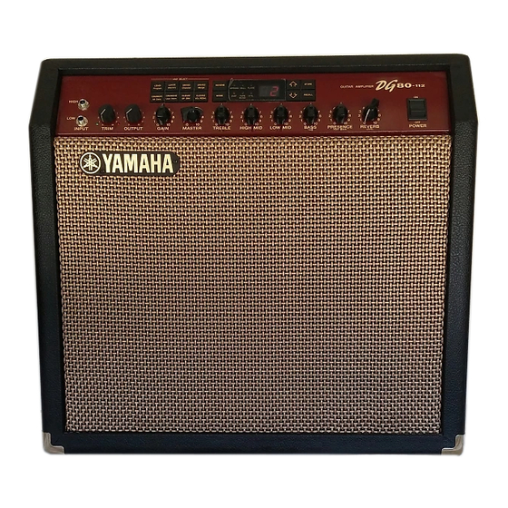
DG80-112 PANEL LAYOUT Front Panel Input Jacks (INPUT HIGH, LOW) Trim Control (TRIM) Output Level Control (OUTPUT) Gain Volume (GAIN) Master Volume (MASTER) Tone Controls (TREBLE, HIGH MID, LOW MID, BASS, PRESENCE) Reverb Volume (REVERB) Amp Select Button/Amp Select Display... -
Page 5: Circuit Board Layout
DG80-112 CIRCUIT BOARD LAYOUT MAIN MAIN MAIN MAIN MAIN MAIN AC cord Power Transformer ANF2 MAIN Power Switch... -
Page 6: Block Diagram
DG80-112 BLOCK DIAGRAM DISASSEMBLY PROCEDURE Pre-Main Unit Remove the four (4) screws marked [70]. The back board (U) can then be removed. (Fig. 1) Remove the plug of the connector assembly (speaker) located on the rear panel and the six (6) screws marked [30A]. -
Page 7: Ground
DG80-112 DM Circuit Board Remove the pre-main unit. (See Procedure 1.) [40] [30C] Remove the two (2) screws marked [150A] and the six (6) screws marked [40c]. The DM [60B] [60B] circuit board can then be removed. (Fig. 3) [50] Power Transformer Remove the pre-main unit. - Page 8 DG80-112 PN Circuit Board VR circuit board assembly Remove the pre-main unit. (See Procedure 1.) [30D] Remove the front panel assembly. (See Procedure 3.) Remove the six (6) screws marked [90]. The PN circuit board assembly can then be removed.
-
Page 9: Lsi Pin Description
DG80-112 LSI PIN DESCRIPTION HD6413002FP16 (XQ375A00) CPU <H8/3002> DM : IC13 NAME FUNCTION NAME FUNCTION Port A Address bus Power supply Address bus Port B Ground P60//WAIT PB6//DREQ0 P61//BREQ Port 6 PB7//DREQ1 /RESO Reset P62//BACK Ground Ø Ø out P90/TXD0... - Page 10 DG80-112 YSS228E-F (XQ962D00) DSP3 (Digital Signal Processor) DM : IC2, 3 NAME FUNCTION NAME FUNCTION Ground Ground DB13 System master clock input (60 M or30 MHz) DB14 System master clock input (60 M or30 MHz) Power supply DB15 /SYNCI System synch. input...
- Page 11 DG80-112 YSF210-M (XK280A00) Digital Filter DM : IC119 NAME FUNCTION NAME FUNCTION OBIT1 Output bit selection System clock OBIT2 22 bit 20 bit 18 bit no output VSS2 Ground OBIT 1 OBIT 2 Bit clock SDSY L/R select and input timing...
-
Page 12: Ic Block Diagram
DG80-112 IC BLOCK DIAGRAM TCHCU04AF-TP1(XD660A00) SN74HC08NSR(XD831A00) TC74VHC32F(XN963A00) Hex Inverter Quad 2 Input AND Quad 2 Input OR DM : IC 101 DM : IC 33 DM : IC 28, 29 TC74HC157AF-TP1(XH603A00) TC74HC164AF(XQ967A00) TC74HC175AF -TP1(XD658A00) Quad 2 to 1 Multiplexer 8-Bit Shift Register... - Page 13 DG80-112 NE5532P(IG102500) NJM072D(IG107000) Dual Operational Amplifier Dual Operational Amplifier DM : IC 104, 105, 124, 125 ANF : IC 501 ANF2 : IC 701 ANR : IC 401 – 403 +DC Voltage Output A Supply Inverting Output B Input A...
-
Page 14: Test Program
2. LED Display Functions SPRING (Error Number) TREBLE : VR603 When the DG80-112 is in the self test mode, the HALL E1 – EE HIGH MID : VR605 LED display shows the number for the status as... - Page 15 “51” and then “52”. When all the LEDs light shows “8”. simultaneously, the MIDI Check is finished. Then the DG80-112 selects the next test no., so the LED (Idling Adjustment) display shows “6”. 1. Set the idling adjustment volume (VR303) at minimum.
- Page 16 DSP-3 and the D/A Converter. [RECALL] key when the LED display shows “9”. The mode of the DG80-112 changes to the normal When the Sound Check is started, the LED display mode and all of the function data are set to the shows “81”.
-
Page 17: Error Messages
Turn off the power and check the circuit for Motor Drive. : MIDI Receive Buffer Full CAUSE: Too much MIDI data is being received by the DG80-112 at one time. SOLUTION: Try reducing the amount of data being sent or, break the data into smaller blocks. -
Page 18: Midi Implementation Chart
DG80-112 YAMAHA [ Digital Guitar Amplifier ] Date:1-Dec-1998 Model DG80-112 MIDI Implementation Chart Version : 1.0 +----------------------------------------------------------------------+ Transmitted Recognized Remarks Function ... : :-------------------+----------------+----------------+----------------: :Basic Default : 1 - 16, off : memorized :Channel Changed : 1 - 16, off... -
Page 19: Circuit Boards
DG80-112 CIRCUIT BOARDS DM Circuit Board MIDI to DM-CN9 Component side Note : See parts list for details of circuit board component parts. ENA-VZ77180-1/10... - Page 20 DG80-112 DM Circuit Board to DM-CN9 Pattern side Note : See parts list for details of circuit board component parts. ENA-VZ77180-2/10...
- Page 21 DG80-112 Panel Layout PN Circuit Board Component side Pattern side VR Circuit Board Note : See parts list for details of circuit board component parts. GAIN MASTER TREBLE HIGH MID LOW MID BASS PRESENCE REVERB TIME FEED BACK LEVEL PN : CNA-V297070-1/5...
-
Page 22: Parts List
DG80-112 ANR Circuit Board MAIN Circuit Board LINE OUT EFFECT LINE OUT SEND RETURN BLEND LEVEL Component side ANF2 Circuit Board ANF Circuit Board Component side HIGH Note : See parts list for details of circuit board Component side component parts. -
Page 23: Parts List
GUITAR AMPLIFIER PARTS LIST CONTENTS OVERALL ASSEMBLY • • • • • • • • • • • • • • • • • • • • • • • • • • • • • • • • • • • • • • • • • • • • • • • • • • • • • • • • • • • • • • • • • • • • • • • • • • • • • • • • • • • • PRE-MAIN UNIT •... - Page 24 DG80-112 OVERALL ASSEMBLY Pre-main unit : See page 4. Overall cabinet assembly : See page 10.
- Page 25 DG80-112 REMARKS PART NO. DESCRIPTION REF NO. RANK OVERALL ASSEMBLY DG80-112 J (V304070) OVERALL ASSEMBLY DG80-112 U (V304080) OVERALL ASSEMBLY DG80-112 E (V304090) OVERALL ASSEMBLY DG80-112 B (V304120) Pre-main Unit (V304030) Pre-main Unit (V304040) Pre-main Unit (V304050) Pre-main Unit (V304060)
- Page 26 DG80-112 PRE-MAIN UNIT AC cord assemdly DM Circuit board assembly Power transformer Chassis assembly : See page 8. 100a Front panel assembly : See page 6. Power switch assembly...
- Page 27 DG80-112 REMARKS PART NO. DESCRIPTION REF NO. RANK PRE-MAIN UNIT DG80-112 J (V304030) PRE-MAIN UNIT DG80-112 U (V304040) PRE-MAIN UNIT DG80-112 E (V304050) PRE-MAIN UNIT DG80-112 B (V304060) Front Panel Assembly (V303830) Front Panel Assembly (V303840) Front Panel Assembly (V303850)
- Page 28 DG80-112 FRONT PANEL ASSEMBLY PN circuit board assembly P100 VR circuit board assembly...
- Page 29 DG80-112 REMARKS PART NO. DESCRIPTION REF NO. RANK FRONT PANEL ASSEMBLY DG80-112 J (V303830) FRONT PANEL ASSEMBLY DG80-112 U (V303840) FRONT PANEL ASSEMBLY DG80-112 E (V303850) FRONT PANEL ASSEMBLY DG80-112 B (V303860) V3034300 Front Panel VR Circuit Board Assembly (V305940)
- Page 30 DG80-112 CHASSIS ASSEMBLY ANR circuit board assembly...
- Page 31 DG80-112 REMARKS PART NO. DESCRIPTION REF NO. RANK CHASSIS ASSEMBLY DG80-112 J (V303990) CHASSIS ASSEMBLY DG80-112 U (V304000) CHASSIS ASSEMBLY DG80-112 E (V304100) CHASSIS ASSEMBLY DG80-112 B (V304200) V3034400 Chassis ANR Circuit Board Assembly (V303760) ANR Circuit Board Assembly (V306410)
- Page 32 DG80-112 OVERALL CABINET ASSEMBLY Handle assembly Front board assembly REMARKS PART NO. DESCRIPTION REF NO. RANK V3063000 OVERALL CABINET ASSEMBLY DG80-112 Cabinet Assembly (V306280) Vinyl (V306320) AA809050 Corner EX808230 Round Head Wood Screw 3.5X16 FNM33G NB812640 Handle Assembly V3062900 Front Board Assembly...
- Page 33 DG80-112 ELECTRICAL PARTS REMARKS PART NO. DESCRIPTION REF NO. RANK ELECTRICAL PARTS DG80-112 VZ771800 Circuit Board (XU331B0) V2979400 Circuit Board (XU365C0) V2979500 Circuit Board (XU365C0) V2979600 Circuit Board (XU365C0) V2979700 Circuit Board (XU365C0) V2978000 Circuit Board (XU365C0) V2978100 Circuit Board...
- Page 34 DG80-112 REMARKS PART NO. DESCRIPTION REF NO. RANK UB245100 Monolithic Ceramic Cap. F 0.100 25V Z C106 C107 UR847100 Electrolytic Cap. 10.00 25.0V C108 UR847100 Electrolytic Cap. 10.00 25.0V C109 UN847100 Electrolytic Cap.-BP 10.00 25.0V C110 UN847100 Electrolytic Cap.-BP 10.00 25.0V...
- Page 35 DG80-112 REMARKS PART NO. DESCRIPTION REF NO. RANK LB918080 Base Post Connector XH 8P TE CN102 VT332900 Diode (chip) 1SS355 TE-17 FZ006970 LC Filter LS MT Y223NB FZ006970 LC Filter LS MT Y223NB EM101 FZ006970 LC Filter LS MT Y223NB...
- Page 36 DG80-112 REMARKS PART NO. DESCRIPTION REF NO. RANK HF757100 Carbon Resistor 10.0K 1/4 J R105 R106 HF757100 Carbon Resistor 10.0K 1/4 J R107 RD255220 Carbon Resistor (chip) 220.0 0.1 J R108 HF756330 Carbon Resistor 3.3K 1/4 J -111 HF756330 Carbon Resistor 3.3K 1/4 J...
- Page 37 DG80-112 REMARKS PART NO. DESCRIPTION REF NO. RANK HF756470 Carbon Resistor 4.7K 1/4 J R609 R610 HF754100 Carbon Resistor 10.0 1/4 J R611 HF756470 Carbon Resistor 4.7K 1/4 J R612 HF754100 Carbon Resistor 10.0 1/4 J R613 HF756470 Carbon Resistor 4.7K 1/4 J...
- Page 38 DG80-112 REMARKS PART NO. DESCRIPTION REF NO. RANK V2978400 Circuit Board ANF2 (XU365C0) V2978700 Circuit Board ANF2 (XU365C0) V2978800 Circuit Board ANF2 (XU365C0) V2978900 Circuit Board ANF2 (XU365C0) C701 VR168700 Monolithic Mylar Capacitor ECQ-V1H224JL3 50V C702 FG652100 Ceramic Capacitor-SL 100P 50V J...
- Page 39 DG80-112 REMARKS PART NO. DESCRIPTION REF NO. RANK HF756220 Carbon Resistor 2.2K 1/4 J R401 R402 HF756220 Carbon Resistor 2.2K 1/4 J R403 HF757120 Carbon Resistor 12.0K 1/4 J R404 HF757100 Carbon Resistor 10.0K 1/4 J R405 HF757100 Carbon Resistor 10.0K 1/4 J...
- Page 40 DG80-112 REMARKS PART NO. DESCRIPTION REF NO. RANK FG644100 Ceramic Capacitor-F 0.0100 50V Z C329 C330 UR847100 Electrolytic Cap. 10.00 25.0V C331 UR847100 Electrolytic Cap. 10.00 25.0V C332 FG644100 Ceramic Capacitor-F 0.0100 50V Z C333 UA355100 Mylar Capacitor 0.1000 50V J...
- Page 41 DG80-112 REMARKS PART NO. DESCRIPTION REF NO. RANK HF758100 Carbon Resistor 100.0K 1/4 J R320 R321 HF755100 Carbon Resistor 100.0 1/4 J R322 HF757680 Carbon Resistor 68.0K 1/4 J R323 HF756470 Carbon Resistor 4.7K 1/4 J R324 HF759220 Carbon Resistor 2.2M 1/4 J...
- Page 42 DG80-112 REMARKS PART NO. DESCRIPTION REF NO. RANK RD257100 Carbon Resistor (chip) 10.0K 0.1 J R209 R210 RD255820 Carbon Resistor (chip) 820.0 0.1 J -212 RD255820 Carbon Resistor (chip) 820.0 0.1 J R213 RD257100 Carbon Resistor (chip) 10.0K 0.1 J...
- Page 43 DG80-112 OVERALL CIRCUIT DIAGRAM 1/2 DM,ANR DG80-112 ASSP Photo Coupler SRAM SRAM W24258 W24258 or SRM2B256 or SRM2B256 DATA SELECTOR DSP3 to PN-CN202 to VR-CN603 BUS BUFFER DRAM BUS BUFFER to PN-CN201 to MAIN1/5-CN308 DSP3 DRAM D-FF D-FF to VR-CN602...
-
Page 44: Parts List
DG80-112 DG80-112 OVERALL CIRCUIT DIAGRAM 2/2 MAIN1/5 5/5,PN,VR,ANF,ANF2 to DM-CN4 to DM-CN5 ANF2 TAPE HIGH UTIL ECHO MOTOR DRIVER OP AMP LEAD1,LEAD2,DRIVE1,DRIVE2 CRUNCH1,CRUNCH2,CLEAN1,CLEAN2 ,STORE,RECALL D-FF SPRING HALL PLATE GAIN MASTER TREBLE HIGH MID LOW MID BASS PRESENCE REVERB (TIME) (FEED BACK)
Need help?
Do you have a question about the DG80-112 and is the answer not in the manual?
Questions and answers