Table of Contents
Advertisement
Quick Links
Note: Please refer to the original service manual for:
DVD Mechanism Unit (DLS6E), Order No. PSG0909002AE
Speaker system SB-PT85EP-K, Order No. PSG1002027CE
TABLE OF CONTENTS
1 Safety Precautions----------------------------------------------- 3
1.1. GENERAL GUIDELINES -------------------------------- 3
1.2. Before Repair and Adjustment ------------------------- 3
1.3. Protection Circuitry ---------------------------------------- 4
1.4. Safety Parts Information --------------------------------- 4
2 Warning -------------------------------------------------------------- 5
to Electrostatic Sensitive (ES) Devices -------------- 5
2.2. Precaution of Laser Diode------------------------------- 6
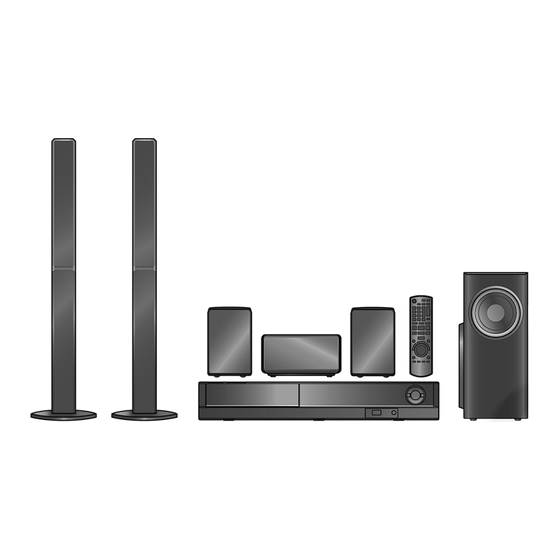
DVD Home Theater Sound System
Model No.
Product Color: (K)...Black Type
PAGE
2.4. Handling Precautions for Traverse Unit --------------8
3 Service Navigation --------------------------------------------- 10
3.1. Service Information -------------------------------------- 10
4 Specifications ---------------------------------------------------- 11
5 Location of Controls and Components------------------ 13
5.1. Remote Control Key Button Operations------------ 13
5.2. Main Unit Key Button Operations -------------------- 14
5.3. Speaker Connection------------------------------------- 14
5.4. Using the VIERA Link "HDAVI Control™"---------- 15
5.5. Disc Information ------------------------------------------ 17
© Panasonic Corporation 2010. All rights reserved.
Unauthorized copying and distribution is a violation
of law.
SA-PT85EE
PSG1002023CE
PAGE
Advertisement
Table of Contents
Troubleshooting

Related Manuals for Panasonic SA-PT85EE


Summary of Contents for Panasonic SA-PT85EE
-
Page 1: Table Of Contents
2.2. Precaution of Laser Diode------------------------------- 6 5.4. Using the VIERA Link “HDAVI Control™”---------- 15 2.3. Service caution based on Legal restrictions -------- 7 5.5. Disc Information ------------------------------------------ 17 © Panasonic Corporation 2010. All rights reserved. Unauthorized copying and distribution is a violation of law. - Page 2 6 Self-Diagnosis and Special Mode Setting -------------- 19 14.2. DVD(Audio/Video) --------------------------------------- 81 6.1. Cold-Start--------------------------------------------------- 19 14.3. DVD(UP-CON) ------------------------------------------- 82 6.2. Service Mode Table-------------------------------------- 19 14.4. System Control ------------------------------------------- 83 6.3. Self-Diagnosis Mode ------------------------------------ 25 14.5. Analog Audio---------------------------------------------- 84 6.4. DVD Self Diagnostic Function-Error Code--------- 26 14.6.
-
Page 3: Safety Precautions
1 Safety Precautions 1.1. GENERAL GUIDELINES 1. When servicing, observe the original lead dress. If a short circuit is found, replace all parts which have been overheated or damaged by the short circuit. 2. After servicing, see to it that all the protective devices such as insulation barriers, insulation papers shields are properly installed. -
Page 4: Protection Circuitry
1.3. Protection Circuitry The protection circuitry may have operated if either of the following conditions are noticed: • No sound is heard when the power is turned on. • Sound stops during a performance. The function of this circuitry is to prevent circuitry damage if, for example, the positive and negative speaker connection wires are “shorted”, or if speaker systems with an impedance less than the indicated rated impedance of the amplifier are used. -
Page 5: Warning
2 Warning 2.1. Prevention of Electrostatic Discharge (ESD) to Electrostatic Sensitive (ES) Devices Some semiconductor (solid state) devices can be damaged easily by static electricity. Such components commonly are called Elec- trostatically Sensitive (ES) Devices. Examples of typical ES devices are integrated circuits and some field-effect transistors and semiconductor “chip”... -
Page 6: Precaution Of Laser Diode
2.2. Precaution of Laser Diode Caution: This product utilizes a laser diode with the unit turned “on”, invisible laser radiation is emitted from the pickup lens. Wavelength: 655 nm (DVD)/790 nm (CD) Maximum output radiation power from pickup: 100 µW/VDE Laser radiation from the pickup unit is safety level, but be sure the followings: 1. -
Page 7: Service Caution Based On Legal Restrictions
2.3. Service caution based on Legal restrictions 2.3.1. General description about Lead Free Solder (PbF) The lead free solder has been used in the mounting process of all electrical components on the printed circuit boards used for this equipment in considering the globally environmental conservation. The normal solder is the alloy of tin (Sn) and lead (Pb). -
Page 8: Handling Precautions For Traverse Unit
2.4. Handling Precautions for Traverse Unit The laser diode in the optical pickup unit may break down due to static electricity of clothes or human body. Special care must be taken avoid caution to electrostatic breakdown when servicing and handling the laser diode in the traverse unit. Cautions to Be Taken in Handling the Optical Pickup Unit 2.4.1. - Page 9 2.4.2.2. Human body grounding 1. Use the anti-static wrist strap to discharge the static electricity form your body. Figure 2...
-
Page 10: Service Navigation
3 Service Navigation 3.1. Service Information This service manual contains technical information which will allow service personnel’s to understand and service this model. Please place orders using the parts list and not the drawing reference numbers. If the circuit is changed or modified, this information will be followed by supplement service manual to be filed with original service manual. -
Page 11: Specifications
0.48 W ® Plays DivX video. Dimensions (W×H×D): 360 mm×58 mm×239 mm MPEG4 data recorded with the Panasonic SD multi cameras Mass: This unit 2 kg or DVD video recorders. 0 °C to +40 °C Operating temperature range: Conforming to SD VIDEO specifications (ASF standard)/... -
Page 13: Location Of Controls And Components
5 Location of Controls and Components 5.1. Remote Control Key Button Operations... -
Page 14: Main Unit Key Button Operations
5.2. Main Unit Key Button Operations Connect USB Device 5.3. Speaker Connection... -
Page 15: Using The Viera Link "Hdavi Control
5.4. Using the VIERA Link “HDAVI Control™”... - Page 16 Home Cinema VIERA Link Control only with TV s remote control This unit s speakers are active. (for HD AVI Control 2 or later ) When you turn on this unit, this unit s speakers will be You can control the playback menus of this unit with the automatically activated.
-
Page 17: Disc Information
5.5. Disc Information 5.5.1. Disc Playability (Media) - Page 18 5.5.2. File Extension Type Support (WMA/MP3/JPEG/MPEG4/DivX)
-
Page 19: Self-Diagnosis And Special Mode Setting
6 Self-Diagnosis and Special Mode Setting 6.1. Cold-Start Here is the procedure to carry out cold-start or initialize to shipping mode. 1. Unplug AC power cord 2. Press & hold [POWER] button 3. Plug AC power cord while [POWER] button being pressed FL Display will show “_ _ _ _ _ _ _ _”... - Page 20 6.2.1. Service Mode Table 1 (For DVD) Item Key Operation FL Display Mode Name Description Front Key Error code Error code check In STOP (no disc) mode, check The latest error code stored in the press [STOP] button on the EEPROM IC is displayed.
- Page 21 6.2.2. Service Mode Table 2 (For DVD) Item Key Operation FL Display Mode Name Description Front Key (Display 1) DVD laser DVD laser drive current measurement. In STOP (no disc) mode, drive current DVD laser drive current is measured press [STOP] button on the measurement and the result is displayed together main unit, and...
- Page 22 6.2.3. Service Mode Table 3 (For DVD) Item Key Operation FL Display Mode Name Description Front Key Micro-processor Micro-processor firmware version In STOP (no disc) (Display 1) firmware version display & EEPROM checksum display. mode, press [STOP] display & EEPROM checksum is only available button on the main unit, EEPROM due to existence of EEPROM IC.
- Page 23 6.2.4. Service Mode Table 4 (For DVD) Item Key Operation FL Display Mode Name Description Front Key DVD Module P.C.B. firmware version is In STOP (no disc) Module P.C.B. displayed on the FL Display. mode, press [STOP] firmware The firmware version can be updated button on the main unit, version display using recovery disc.
- Page 24 Product Region TV Broadcasting Model Series Country Region Signal System Region Display Code System OSD Menu Language Default (Default) (Default) USA, Canada, English (NA), Spanish (NA), P, PC, PX NTSC NTSC (*A) English US Militry Canadian, French Japan NTSC NTSC (*A) Japanese Japanese, English English (EU), French, German,...
-
Page 25: Self-Diagnosis Mode
6.3. Self-Diagnosis Mode Item Key Operation FL Display Mode Name Description Front Key Self-Diagnostic To enter into self-diagnostic checking Press & hold [STOP] on main Mode for DLS6E Mechanism unit, follow by [4] then [9] on remote control. (When no disc in mechanism) Error code will display Error code... -
Page 26: Dvd Self Diagnostic Function-Error Code
6.4. DVD Self Diagnostic Function-Error Code 6.4.1. Mechanism Error Code Table Error Diagnosis Contents Description of error Automatic FL Display Remarks Code H01 Tray loading error The tray opening and closing is abnormal. Press [ STOP] on main CLOSE and OPEN of the tray cannot be unit for next error. - Page 27 6.4.2. DVD Module Error Code Table Error Diagnosis Contents Description of error Automatic FL Display Remarks Code U702 HDMI/DVI I2C The communication error of I2C when Press [ STOP] on main communication error connecting it with HDMI/DVI. For unit for next error. instance, when EDID information to which information on the TV set side has been described cannot be read, it is generated.
- Page 28 6.4.3. Power Supply & Digital Amplifier Error Code Table Error Diagnosis Contents Description of error Automatic FL Display Remarks Code F61 The abnormalities In normal operation, when DCDET2 goes Press [ STOP] on main in the D-Amp related to "L" (Low) (Not during POWER OFF unit for next error.
-
Page 29: Sales Demonstration Lock Function
6.5. Sales Demonstration Lock Function This function prevents discs from being lost when the unit is used for sales demonstrations by disabling the disc eject function. “LOCKED” is displayed on the unit, and ordinary operation is disabled. 6.5.1. Setting • Prohibiting removal of disc 1. -
Page 30: Firmware Version-Up Information
6.6. Firmware Version-Up Information 6.6.1. Process Flow (1/3) Item FL/ GUI Display Remarks Process Description Collect ROM There are 2 files: User can put both files Files A) Syscon ROM file type: into the same root (Copy files into Display 1: directory. -
Page 31: Process Flow
6.6.2. Process Flow (2/3) Item FL/ GUI Display Remarks Process Description GUI Display 1.3.2: GUI Display 1.3.2: UPDATING WRITING TO FLASHROM FL Display 2: Update stop Check Correct ROM files doesn’t fit to the (Wrong ROM Type) ROM file type product type. - Page 32 6.6.3. Process Flow (3/3) Item FL/ GUI Display Remarks Process Description 1. Update Failed Update software Update stop. FL Display 4: (Opecon) The theater set can’t work, If Opecon software update fail: and can’t be recovered by FL Display 3: "FAIL" . CD update again.
-
Page 33: Troubleshooting Guide
7 Troubleshooting Guide 7.1. Troubleshooting Guide for F61 and/or F76 This section illustrates the checking procedures when upon detecting the error of “F61” and/or “F76” after power up of the unit. It is for purpose of troubleshooting and checking in SMPS, D-Amp & Main P.C.B. 7.1.1. - Page 34 7.1.2. Troubleshooting Guide...
-
Page 35: Switching Regulator
7.1.3. Part Location 7.1.3.1. SMPS P.C.B. Shunt Regulator: IC5801 Switching Regulator Switching Regulator L5701 Diode: D5802 IC: IC5701 Switching L2910, L2915, TH5702 L5702 Diode: Transformer: L2916, FP2901 D5701 T2900 Feedback Circuit: PC5720, D5725... -
Page 36: Main/D-Amp P.c.b
7.1.3.2. Main/D-Amp P.C.B. Switching Regulator Digital Amplifier IC: Open Circuit: IC: IC106 IC403, IC404, IC405 IP100 DAP IC: IC401 Regulator Circuit: Q107... -
Page 37: Basic Troubleshooting Guide For Traverse Unit (Dvd Module P.c.b.)
7.2. Basic Troubleshooting Guide for Traverse Unit (DVD Module P.C.B.) Problems Checking Points Checking components 1) Distorted picture or a) Check SDRAM address, data IC8051 abnormal sound is head bus, CLK and other control signals during the initialization waveform b) Check video signals (Y,C) LB8315, R8321, LB8316, R8325... -
Page 38: Basic Troubleshooting Guide For Hdmi Av Output
7.3. Basic Troubleshooting Guide for HDMI AV output Problems Checking Points Checking components 1) TV does not have any 1) Check setting of the set in * This year HDMI always ON. display. Set FL display Setup Menu whether the HDMI No need check Setup Menu. - Page 39 Problems Checking Points Checking components 1) TV does not have any 13) Hot-Plug Signal LB3906, R3902, R3903, Q3901, D3901 display. Set FL display shows U702/U703 14) TDMS Output swing amplitude R3901 control resistor 15) Host Interface External Input LB8702 Clock from LSI (IC8001) to Up-Con IC (IC3901) - OSC27M 16) Video Data Lines from LSI RX3707, RX3708, IC3901...
-
Page 40: Disassembly And Assembly Instructions
8 Disassembly and Assembly Instructions “ATTENTION SERVICER” Be careful when disassembling and servicing. Some chassis components may have sharp edges. Special Note: 1. This section describes the disassembly procedures for all the major printed circuit boards and main components. 2. Before the disassembly process was carried out, do take special note that all safety precautions are to be carried out. -
Page 41: Disassembly Flow Chart
8.1. Disassembly Flow Chart 8.3. Top Cabinet 8.6. DVD Mechanism 8.4. Component Video Unit (DLS6E) P.C.B. 8.5. Rear Panel 8.7. DVD Module P.C.B. 8.13. Front Panel 8.8. SMPS P.C.B. Assembly 8.9. Switching Regulator 8.14. FL P.C.B. IC (IC5701) 8.15. Volume Button 8.10. -
Page 42: Main Components And P.c.b. Locations
8.2. Main Components and P.C.B. Locations... -
Page 43: Disassembly Of Top Cabinet
8.3. Disassembly of Top Cabinet Step 1 Remove 2 screws at the side of Top Cabinet Step 2 Remove 3 screws at the rear of Top Cabinet. Step 6 Remove Top Cabinet as arrow shown. Step 3 Lift up the back portion of Top Cabinet as arrow shown. 8.4. -
Page 44: Disassembly Of Rear Panel
Caution: During assembling, ensure that Component Video P.C.B. is properly located & fully catched onto rear panel. Step 3 Lift up to remove Component Video P.C.B.. 8.5. Disassembly of Rear Panel • Refer to “Disassembly of Component Video P.C.B.”. Step 1 Remove 6 screws. Step 2 Remove 1 screw. -
Page 45: Disassembly Of Dvd Mechanism Unit (Dls6E)
Step 4 Remove Rear Panel. Step 4 Detach 7P FFC at the connector (FP8251) on DVD Module P.C.B.. Step 5 Lift up cover of connector (FP8531) to detach 24P FFC at the connector on DVD Module P.C.B.. Caution: Ensure FFC is inserted properly before closing the cover of the connector. -
Page 46: Disassembly Of Dvd Module P.c.b
Step 3 Detach 5P wire at the connector (FP9001) on DVD Module P.C.B.. Caution: During assembling, ensure that DVD Mechanism Unit (DLS6E) is properly located and fully seated on bot- tom chassis before screwing. Caution: Ensure that two guiding pins of DVD Mechanism Unit (DLS6E) are fully inserted into the two slots of Front Panel Assembly. -
Page 47: Disassembly Of Smps P.c.b
Caution: During assembling, ensure that DVD Module P.C.B. is properly located & fully seated onto bottom chas- sis. Step 3 Remove 4 screws. 8.8. Disassembly of SMPS P.C.B. • Refer to “Disassembly of Top Cabinet”. • Refer to (Step 1) to (Step 3) of item 8.5. Step 1 Position Rear Panel according to diagram shown. -
Page 48: Replacement Of Switching Regulator Ic (Ic5701)
Caution: Handle the SMPS P.C.B. with care. Avoid touching the heatsink due to its prolong use. Caution: During assembling, ensure that SMPS P.C.B. is Step 2 Remove 1 screw from the Switching Regulator IC properly located & fully inserted onto Bottom Chassis. (IC5701). -
Page 49: Replacement Of Diode (D5802)
Caution: Ensure the Switching Regulator IC (IC5701) is tightly screwed to the Heatsink Ext A. Step 2 Remove 1 screw from the Diode (D5802). Step 4 Solder pins of the Switch Regulator IC (IC5701) on the Step 3 Remove the Diode (D5802) from the Heatsink Ext B. solder side of SMPS P.C.B.. -
Page 50: Disassembly Of Main/D-Amp P.c.b
Caution: Ensure the Diode (D5802) is tightly screwed to the Heatsink Ext B. Step 2 Detach 17P FFC at the connector (CN203) on Main/D- Amp P.C.B.. Step 4 Solder pins of the Diode (D5802) on the solder side of SMPS P.C.B.. Step 3 Detach 15P Cable Wire at the connector (CN103) on 8.11. -
Page 51: Replacement Of Digital Amplifier Ic (Ic403/ Ic404/Ic405)
Caution: During assembling, ensure that Main/D-Amp P.C.B. is properly located & fully seated onto Bottom Chas- sis. Step 4 Remove 2 screws on Main/D-Amp P.C.B.. 8.12. Replacement of Digital Ampli- Step 5 Remove 1 screw on Main/D-Amp P.C.B.. fier IC (IC403/IC404/IC405) •... - Page 52 Caution: Handle the Main/D-Amp P.C.B. with caution due to 8.12.2. Assembly of Digital Amplifier IC its high temperature after prolonged use. Touching it may (IC403/IC404/IC405) lead to injuries. Step 3 Remove Digital Amplifier IC (IC403) by desolder its pins. Step 1 Mount & Solder the pins of Digital Amplifier IC (IC403) Note: For disassembling of Digital Amplifier IC (IC404/ on to the Main/D-Amp P.C.B..
-
Page 53: Disassembly Of Front Panel Assembly
Caution: Ensure that Main/D-Amp P.C.B. is properly Caution: Replace the tesa tape if it is torn. located and fixed on to Amp Heatsink before screwing. Caution: During assembling, replace the IC insulator if it is broken. Step 5 Release the 2 tabs at each side of the Front Panel Assembly in the direction of arrow. -
Page 54: Disassembly Of Fl P.c.b
Caution: Do not exert strong force when releasing the tabs. Caution: During assembling, ensure that 5P wire is dressed between bottom chassis and front panel properly according to diagram shown. Step 7 Remove Front Panel Assembly. 8.14. Disassembly of FL P.C.B. •... -
Page 55: Disassembly Of Volume Button P.c.b
Caution: Keep the Ground Spring in safe place, place it Caution: During assembling, ensure that FL P.C.B. is prop- back during assembling. erly located and fully fixed onto front panel. Caution: During assembling, ensure that 5P wire is dressed properly according to diagram shown. Step 5 Desolder 3P Cable at the cable holder (H902) on FL P.C.B.. -
Page 56: Disassembly Of Power Button P.c.b
Step 4 Remove Volume Button P.C.B.. Caution: During assembling, ensure that Power Button P.C.B. is fully catched. Step 3 Lift up Power Button P.C.B.. Caution: During assembling, ensure that Volume Button P.C.B. is properly located & fully seated onto Front Panel. Caution: During assembling, ensure that 3P cable is dress properly. -
Page 57: Replacement Of Dvd Lid Assembly
Caution: During assembling, ensure that Power Button P.C.B. is properly located & fully catched onto Front Panel with 3P cable dressed according to diagram shown. Step 3 Lift the door spring at Shaft A in the direction of arrow. 8.17. Replacement Assembly •... - Page 58 Step 2 Fully release Door Spring from DVD Lid Assembly and to be rested onto Front Panel. Caution: Ensure that Shaft A of DVD Lid Assembly is fully inserted into Slot A of Front Panel. Step 5 Remove DVD Lid Assembly. Assembly of DVD Lid Assem- 8.17.2.
- Page 59 Caution: Ensure that Shaft B of DVD Lid Assembly is fully inserted into Slot B of Front Panel.
-
Page 60: Assembling And Disassembling Of Traverse Unit
9 Assembling and Disas- sembling of Traverse Unit 9.1. Disassembly of Traverse Unit • Refer to “Disassembly of DVD Mechanism Unit (DLS6E)” Step 1 Release the guide and slide the traverse slide plate (rib) as arrows shown. Step 3 Slide out the Traverse unit as arrow shown. Caution: Do not touch the surface of the Traverse unit and place it so that the OPU is on top. - Page 61 Step 4 Release the guide and slide the traverse slide plate (rib) in the direction of arrows shown to lock in the traverse unit. Step 2 Slot the traverse unit approximately 45° into the mecha chassis as arrow shown. Note: Ensure the bosses fix exactly onto the guides. Step 3 Place down the traverse unit as arrow shown.
-
Page 62: Service Position
10 Service Position Note: For description of the disassembly procedures, see the Section 8. 10.1. Checking & Repairing Main/D- P.C.B. & Component Video P.C.B. Step 1 Remove Top Cabinet. Step 2 Remove Main/D-Amp P.C.B.. Step 3 Remove Amp Heatsink. Step 4 Attach 15P Cable wire at the Connector (CN103) on Main P.C.B.. -
Page 63: Checking & Repairing Of Fl P.c.b
Caution: Handle the SMPS P.C.B. with care. Avoid touching the heatsink due to its prolong use. Step 5 Remove Ground Spring. Step 6 Release 2 catches on Power Button P.C.B.. Step 8 Position SMPS P.C.B. as diagram shown. Step 7 Remove FL P.C.B., Volume Button P.C.B. and Power Step 9 Proceed to check and repair SMPS P.C.B.. -
Page 64: Checking & Repairing Of Dvd Module P.c.b
10.4. Checking & Repairing of DVD Module P.C.B. 10.4.1. Checking & Repairing of Side B of DVD Module P.C.B. Step 1 Remove Component Video P.C.B.. Step 2 Remove Front Panel Assembly. Step 3 Slightly move DVD Mechanism Unit (DLS6E) forward according to diagram shown. -
Page 66: Voltage & Waveform Chart
IC3901 REF NO. MODE CD PLAY REF NO. IC3952 MODE CD PLAY IC8001 REF NO. MODE CD PLAY IC8001 REF NO. MODE CD PLAY IC8001 REF NO. MODE CD PLAY IC8001 REF NO. MODE CD PLAY SA-PT85EE DVD MODULE P.C.B. -
Page 67: Dvd Module P.c.b. (2/4)
REF NO. IC8001 MODE CD PLAY IC8051 REF NO. MODE CD PLAY IC8051 REF NO. MODE CD PLAY IC8051 REF NO. MODE CD PLAY IC8111 REF NO. MODE CD PLAY IC8251 REF NO. MODE CD PLAY SA-PT85EE DVD MODULE P.C.B. -
Page 68: Dvd Module P.c.b. (3/4)
IC8701 REF NO. MODE CD PLAY IC8901 REF NO. MODE CD PLAY REF NO. IC9001 MODE CD PLAY IC9002 REF NO. MODE CD PLAY IC9003 REF NO. MODE CD PLAY IC9006 REF NO. MODE CD PLAY SA-PT85EE DVD MODULE P.C.B. -
Page 69: Dvd Module P.c.b. (4/4)
11.4. DVD Module P.C.B. (4/4) Q3901 Q3902 Q3903 Q3941 Q3942 REF NO. MODE CD PLAY Q3943 Q8551 Q8552 Q8561 Q8562 REF NO. MODE CD PLAY Q8563 Q8564 Q8565 REF NO. QR9030 MODE CD PLAY SA-PT85EE DVD MODULE P.C.B. -
Page 70: Main/D-Amp P.c.b. (1/3)
CD PLAY STANDBY REF NO. IC200 MODE CD PLAY STANDBY IC200 REF NO. MODE CD PLAY STANDBY REF NO. IC200 MODE CD PLAY STANDBY IC201 REF NO. MODE CD PLAY STANDBY IC202 REF NO. MODE CD PLAY STANDBY SA-PT85EE MAIN/D-AMP P.C.B. -
Page 71: Main/D-Amp P.c.b. (2/3)
CD PLAY STANDBY IC404 REF NO. MODE CD PLAY 10.1 20.3 20.3 20.3 10.2 10.2 20.3 20.3 STANDBY 10.1 20.3 20.3 20.3 10.2 10.2 20.3 20.3 IC404 REF NO. MODE CD PLAY 20.3 10.2 STANDBY 20.3 10.2 SA-PT85EE MAIN/D-AMP P.C.B. -
Page 72: Main/D-Amp P.c.b. (3/3)
Q108 Q109 Q114 Q116 MODE CD PLAY 20.1 STANDBY 20.1 Q121 Q203 Q500 Q501 REF NO. MODE CD PLAY 10.0 10.0 10.0 10.0 STANDBY REF NO. Q2011 MODE CD PLAY -5.0 -24.7 -5.6 STANDBY -5.0 -24.7 -5.6 SA-PT85EE MAIN/D-AMP P.C.B. -
Page 73: Fl P.c.b
-22.4 -24.7 -24.7 -17.8 -17.8 -24.7 -24.7 -15.7 -17.9 -25.2 -19.0 -24.8 -22.7 -22.7 -22.7 -22.7 -22.7 -22.7 -22.7 -22.7 IC901 REF NO. MODE CD PLAY -22.6 -22.6 STANDBY -22.7 -22.7 SA-PT85EE FL P.C.B. 11.9. SMPS P.C.B. IC2900 REF NO. MODE CD PLAY 20.3 11.9 STANDBY 20.3 11.9... -
Page 74: Component Video P.c.b
11.10. Component Video P.C.B. IC4101 REF NO. MODE CD PLAY STANDBY IC4101 REF NO. MODE CD PLAY STANDBY Q4001 REF NO. MODE CD PLAY STANDBY SA-PT85EE COMPONENT VIDEO P.C.B. -
Page 75: Waveform Table (1/3)
11.11. Waveform Table (1/3) 0.4Vp-p(500usec/div) 3.2Vp-p(20nsec/div) 2Vp-p(20nsec/div) 2Vp-p(20nsec/div) 1Vp-p(20nsec/div) 3.2Vp-p(500nsec/div) 3.6Vp-p(500nsec/div) 6Vp-p(1usec/div) 1.6Vp-p(1usec/div) 3.4Vp-p(2usec/div) 6Vp-p(1usec/div) 6Vp-p(500nsec/div) 0.4Vp-p(500usec/div) 0.68Vp-p(10usec/div) 1Vp-p(20usec/div) 0.6Vp-p(20usec/div) 0.48Vp-p(20usec/div) 3.8Vp-p(5msec/div) 2Vp-p(20usec/div) 6.4Vp-p(5usec/div) -
Page 76: Waveform Table (2/3)
11.12. Waveform Table (2/3) 6.4Vp-p(5usec/div) 6Vp-p(5usec/div) 6.8Vp-p(5usec/div) 6.4Vp-p(5usec/div) 6.8Vp-p(5usec/div) 6.4Vp-p(5usec/div) 6.4Vp-p(5usec/div) 0.4Vp-p(500nsec/div) 1.1Vp-p(20usec/div) 5.2Vp-p(500nsec/div) 0.76Vp-p(10usec/div) 0.8Vp-p(10usec/div) 1Vp-p(20usec/div) 5.6Vp-p(2usec/div) 6Vp-p(1usec/div) 1.5Vp-p(500usec/div) 0.15Vp-p(500usec/div) 9.2Vp-p(500nsec/div) 1.5Vp-p(20nsec/div) 0.64Vp-p(500nsec/div) -
Page 77: Waveform Table (3/3)
11.13. Waveform Table (3/3) 0.84Vp-p(500nsec/div) 8Vp-p(50nsec/div) 0.8Vp-p(500nsec/div) 0.8Vp-p(500nsec/div) 1.2Vp-p(500nsec/div) 0.6Vp-p(500nsec/div) 0.8Vp-p(500nsec/div) 1Vp-p(500nsec/div) 0.8Vp-p(500nsec/div) -
Page 78: Illustration Of Ics, Transistor And Diode
12 Illustration of ICs, Transistor and Diode C0ABBB000244 (8P) RFKWMH42B3D2(48P) RFKWMPT85EP VUEALLPT040 (20P) REPX0762E (8P) C3EBFY000006 (8P) (100p) C1AB00003216 (64P) C0FBAK000026 (16P) C0HBB0000057 (44P) C0JBAR000540 (16P) MN864702A (128P) C0JBAZ002999 (20P) MN2DS0018MP (216P) C9ZB00000584 (32P) No.1 No.1 No.1 C1AB00003217 (44P) No.1 C3ABPG000160 (54P) C0GBG0000048 (30P) C0CBCDC00063... -
Page 79: Overall Simplified Block Diagram
13 Overall Simplified Block Diagram Tuner Reset/Data/CLK /VALID DIGITAL AMP BLOCK six channel BTL output TUNER PACK FRONT L FL+/- HOTPLG/CECIN HDMI CECOUT 4CH ANALOG SELECTOR FRONT R FR+/- SCART AUDIO IN V+5V VIDEO BUFFER SL+/- SURR L A+5V Digital AUDIO PROCESSOR 2CH ADC SR+/- ANALOG SELECTOR CONTROL... -
Page 80: Block Diagram
103 LPC1 105 LPC2 SP DRV VIN3 LEVEL DRV1 66 SPINDLE SHIFTER MOTOR VO3- FP8251 OPIN- OPOUT AD1 122 OPIN+ ACTUATOR FP8531 VO1+ TRACKING COIL LEVEL SHIFTER FP8531 VO1- FP8531 VO2+ FOCUS COIL LEVEL SHIFTER FP8531 VO2- SA-PT85EE DVD(SERVO) BLOCK DIAGRAM... -
Page 81: Dvd(Audio/Video)
CN201 FROM/TO AOUT0 DRV3 64 FP8531 VIN10 DIGITAL AUDIO 111 VIN10 FP8101 CN201 AOUT1 DRV4 63 FP8531 AOUT2 FP8101 CN201 96 RFINP DRV5 62 DMIXOUT FP8101 CN201 ADOUT 151 JK8001 OPTICAL IECINPUT OUT 3 75 EXTRG1 SA-PT85EE DVD(AUDIO/VIDEO) BLOCK DIAGRAM... -
Page 82: Dvd(Up-Con)
AND GATE NRESET NRST 70 1 IN1 TXRST NRESET HDMIRST TRCDATATA2 79 2 IN2 HOTPLG FG 71 MAIN/D-AMP P.C.B Q3941, Q3942, Q3943 CN201 FP8101 CEC IN FROM/TO CEC CIRCUIT SYSTEM CONTROL 13 CEC CN201 FP8101 CEC OUT SA-PT85EE DVD(UP-CON) BLOCK DIAGRAM... -
Page 83: System Control
ANALOG AUDIO TUN SCLK TUN SCLK TUN SCLK SEL A SEL A SEL A SEL B SEL B SEL B Q121 CN201 FP8101 CEC IN BUFFER FROM/TO DVD(UP-CON) CN201 FP8101 CEC OUT COMPONENT VIDEO P.C.B SA-PT85EE SYSTEM CONTROL BLOCK DIAGRAM... -
Page 84: Analog Audio
CN203 CN201 FP8101 MPORT RCH RECOUT-L 11 R3 L CH 3 MLCH CN901 CN203 DVD(AUDIO/VIDEO) MPORT LCH RECOUT-R CN201 FP8101 4 L3 R CH 13 MPORT SW H902 H901* SYSTEM CONTROL IC2105 C0JBAR000540 4CH MULTIPLEXER SA-PT85EE ANALOG AUDIO BLOCK DIAGRAM... -
Page 85: Digital Audio
SP FR+ OUT D 28 (RIGHT) 17 RST CD(L) BST D 24 FROM/TO SYSTEM CONTROL VALID VALID VALID ECO DAMP ECO SUPLLY ECO DAMP CIRCUIT Q114 Q116 DC DET2 SP PROTCT DC DET2 DC DETECT SWITCH SA-PT85EE DIGITAL AUDIO BLOCK DIAGRAM... -
Page 86: Analog Video
CB/PB/B CBIN 13.5MHz BIAS CBOUT 75Ohm CBSAG BIAS BIAS SEL3 75Ohm FP8302 CN4002 CROUT CR/PR/R CRIN 13.5MHz BIAS CRSAG S-DCOUT SDCOUT S1/S2 Q4001 FROM FP8302 CN4002 MUTING VMUTE 5 MUTE1 SYSTEM CONTROL CONTROL 14 MUTE2 SA-PT85EE ANALOG VIDEO BLOCK DIAGRAM... -
Page 87: Power Supply
FB 6 GND 3 Q5841 DCDET H2016* CN103 DC DET1 DC DETECT H2016* CN103 PC5720 FEED BACK Q5863 FROM FEED BACK H2016* CN103 ECO CTL CIRCUIT SYSTEM CONTROL IC5801 C0DAEMZ00001 SHUNT REGULATOR COLD MAIN/D-AMP P.C.B SA-PT85EE POWER SUPPLY(1/2) BLOCK DIAGRAM... - Page 88 COMPONENT VIDEO P.C.B SW5V IC8111 C0DBFZG00001 IC107 SWITCHING C0CBABC00117 REGULATOR VOLTAGE REGULATOR D3.3V +3.3V 1 VCC D3.3V 6 SW5V D3.3V +3.3V 3 IN OUT 1 NSW1.2V +1.2V 3 VCC 1.2V 7 V+5V CN201 FP8101 FP8302 CN4002 SA-PT85EE POWER SUPPLY(2/2) BLOCK DIAGRAM...
-
Page 89: Wiring Diagram
POWER BUTTON P.C.B. HDMI (AV OUT) (SOLDER SIDE) FP8031* COMPONENT VIDEO P.C.B. H901* (SOLDER SIDE) JK4002 CN4002 COMPONENT VIDEO OUT/ VIDEO OUT FOR SOFTWARE TO OPTICAL PICKUP UNIT NOTE: " * " REF IS FOR INDICATION ONLY. SA-PT85EE WIRING CONNECTION... -
Page 91: Schematic Diagram Notes
16 Schematic Diagram Notes • Voltage and signal line : +B signal line • This schematic diagram may be modified at any time : -B signal line with the development of new technology. : Audio output signal line Notes: : Video output signal line S901: Open/Close switch ( ). -
Page 93: Schematic Diagram
VIN8 SPMUTE VIN1 EXADR_16 FEXDT_15 VIN7 D8211 TRVFTMUTE VIN4 MA2J1110GL [107]AVDDB [55]P8 VIN6 VIN3 [56]P9 [108]AVSSB VIN5 C8211 R8211 VIN9 1200P VIN9 C8022 VIN10 VDD33 VIN10 CPU-CMD VHALF CPU-STAT VREFH 56 57 TO DVD MODULE(DV5U) SA-PT85EE SECTION (3/4) MODULE(DV5U) CIRCUIT... - Page 94 K8118 DMIXOUT 2.4K R8311 CPU-CLK K8691 K8119 R8335 AOUT0 AOUT0 K8120 AOUT1 K8121 AOUT1 R8312 AOUT2 C8311 AOUT2 CR_PR_R K8341 CPU-STAT DAC3OUT TO DVD MODULE(DV5U) SA-PT85EE R8341 SECTION (4/4) DOP_CPU-STAT DVD MODULE(DV5U) CIRCUIT LB8692 TO DVD MODULE(DV5U) SECTION (1/4) K8695...
- Page 95 TXRST TXRST MDQ_14 MDQ_1 DQ14 C8052 R8602 VSSQ VDDQ D+3R3V D+3R3V MDQ_15 MDQ_0 SA-PT85EE DQ15 C8901 MODULE(DV5U) CIRCUIT D+3R3V DV: DVD MODULE(DV5U): SCHEMATIC DIAGRAM 1 - 4 HOTPLG HD: DVD MODULE(HDMI): SCHEMATIC DIAGRAM - 5 HOTPLG C8051 V_CLK R8901 VCLK...
- Page 96 HD: DVD MODULE(HDMI): SCHEMATIC DIAGRAM - 5 CD-LD LPC1 R8531 1.5K R8538 R8539 C8531 100P R8536 K8004 K8009 Q8563 R8535 100K B1CFHA000002 DVD-LD SWITCH GND-LD R8533 R8534 Q8565 LPC2 R8532 2.2K B1ABDF000026 Q8564 INVERTER B1CFHA000002 C8532 R8537 220P SA-PT85EE SWITCH MODULE(DV5U) CIRCUIT DVD_CD...
- Page 97 HD: DVD MODULE(HDMI): SCHEMATIC DIAGRAM - 5 Q3903 B1CFHA000002 R3906 LEVEL SHIFTER 4.7K R3945 IC3952 TXRST TXRST OSC27M C0CBCDC00063 OSC27M I2C_SCL VOLTAGE REGULATOR I2C_SCL I2C_SDA I2C_SDA RX3901 C3955 D1H410120001 0.01 VCLK R3947 VCLK HOTPLG HOTPLG K3903 M+9V M+9V SA-PT85EE DVD MODULE(HDMI) CIRCUIT...
-
Page 98: Main/D-Amp Circuit
2.7K C120 TUN_R C3207 R125 R130 Q2011 R2010 R126 B1ADCE000012 C3208 C3206 C3205 -5V REGULATOR 330P 1000P R127 L428 G0A200D00002 MPORT_R C118 Q108 Q109 R3208 B1GBCFJJ0051 B1GBCFJJ0051 INVERTER INVERTER R3207 5.6K MPORT-RCH AGND TO MAIN/D-AMP SA-PT85EE SECTION (4/6) MAIN/D-AMP CIRCUIT... - Page 99 DVD_STAT K110 DOP_CPU_STAT R214 DVD_CMD K111 DOP_CPU_CMD DVD_CLK L100 J0JBC0000015 DOP_CPU_CLK R204 Q102 D3.3V B1ADCE000012 R205 TRAY_CCW_L SWITCH SYS5VGND R134 R146 VREF 2.2K R133 CNVSS Q103 2.2K TRAY_CW_H RESET 2SD0601AHL K158 TO MAIN/D-AMP SWITCH SECTION (5/6) SA-PT85EE MAIN/D-AMP CIRCUIT CHASSIS...
- Page 100 SP_FR+ C519 PVDD_D 25V470 C520 C455 C171 L409 0.47 0.01 1000P G0A100H00018 R452 C510 0.033 BST_D R506 R453 GVDD_C GVDD_D SP_SL- C190 1000P C433 C432 C431 C514 C567 16V10 1000P K157 R454 CHASSIS TO MAIN/D-AMP SECTION (6/6) SA-PT85EE MAIN/D-AMP CIRCUIT...
- Page 101 [3] PLL_FLTM [17] VRD_DPLL PWM_HPPR XTL_OUT MCLK X400 R495 MCLK OSC_CAP H0J135000003 RESERVED C415 C412 10 11 12 13 C400 IC107 C0CBABC00117 VOLTAGE REGULATOR C411 C401 R400 C453 0.01 L425 L426 C451 C418 C419 C452 L427 J0JBC0000015 SA-PT85EE MAIN/D-AMP CIRCUIT...
- Page 102 VREF FL CIRCUIT K134 D116 B0JCPG000005 FLD_OUT K135 (CN901) FL_IC_DAT K162 K163 K103 K101 K105 FLD_CLK IN SCHEMATIC K136 FL_IC_CLK FLD_STB K137 DIAGRAM - 12 FL_IC_STB KEY2 K138 KEY2 K139 KEY1 KEY1 K131 FL_GND K128 K129 K130 SA-PT85EE MAIN/D-AMP CIRCUIT...
- Page 103 Q116 220K SP_PROTCT B1ADBL000010 SWITCH R178 Q114 B1ABCF000011 R184 5.6K SP_FR+ DC DETECT R587 D118 C151 R176 B0ACCK000005 50V1 5.6K ECO_DAMP SP_FL+ R175 5.6K SP_SUB+ C153 D119 100K B0ACCK000005 L422 J0JKB0000020 L421 J0JKB0000020 C150 K159 25V1000 ZJ159 SA-PT85EE MAIN/D-AMP CIRCUIT...
-
Page 104: Fl, Volume Button & Power Button Circuit
S905 S901 2.2K TUNE DOWN R915 R906 R907 OPEN/CLOSE 1.5K H901* S906 R913 DGND R908 S902 TUNE UP 1.5K 1.2K POWER MPORT KEY1 H903 R914 S907 1.2K PLAY DGND KEY2 DGND SA-PT85EE FL / VOLUME BUTTON / POWER BUTTON CIRCUIT... -
Page 105: Component Video Circuit
MUTE2 GND2 C4010 C4016 6.3V470 CRIN CROUT VCC2 CRSAG JK4002 C2826 C2827 R2816 L2805 J0JBC0000015 [CR] COMPONENT R2813 L2804 VIDEO OUT J0JBC0000015 [CB] R2812 L2803 VIDEO OUT J0JBC0000015 R2809 L2802 J0JBC0000015 COMPONENT VIDEO OUT C2823 C2825 SA-PT85EE COMPONENT VIDEO CIRCUIT... -
Page 106: Smps Circuit
R5730 R5808 2.2K R5802 C5810 D5725 B0BC6R2A0266 R5803 2.7K R5804 IC5801 R5806 2.7K C0DAEMZ00001 C5818 SHUNT REGULATOR TO SMPS SECTION (2/2) R5801 2.7K Q5863 B1ABCF000176 R5865 4.7K SWITCH R5829 C5864 R5866 C5870 C5820 R5817 100K 0.01 6.3V2200 SA-PT85EE SMPS CIRCUIT... - Page 107 R5725 R5724 SECTION (1/2) 2200P C5720 C5725 OLP/SS 1000P R5733 D5722 ZJ5700 B0BC018A0267 D5729 B0EAMM000057 C5722 C5700 K5721 C5730 D5726 2200P R5732 F1BAF2220023 D5732 MA2J1110GL 2200P MAZ83000ML C5721 C5726 D5723 C5747 220P 50V10 MA2J1110GL 560P R5726 0.27 SA-PT85EE SMPS CIRCUIT...
-
Page 108: Printed Circuit Board
C9002 C3910 R8555 K3903 R8558 R9009 R9008 C3954 R8554 R9085 IC9003 Q3943 R3945 Q8552 R3944 R3941 R3943 LB3907 LB3908 IC3952 Q8551 R3942 K8116 Q3942 Q3941 C8551 K8117 C8554 0640A-1 0640A-1 0640A-1 0640A-1 (SIDE A) (SIDE B) SA-PT85EE DVD MODULE P.C.B. -
Page 109: Main/D-Amp P.c.b
C472 C186 C192 R525 R176 C191 C522 C187 K101 C501 C190 C189 C188 R274 C558 R280 D203 C540 R275 R276 K13...PT85 LB51 K21...EE C130 K130 K141 K143 K128 K142 K129 K131 K116 K140 0644A-1 0644A-1 (SIDE A) SA-PT85EE MAIN/D-AMP P.C.B. - Page 110 3 2 1 IC52 IC2105 K110 L428 K145 L101 C3208 C3108 4 5 6 C123 K144 Q102 Q103 R146 C118 R143 R144 R130 K125 C117 R142 R133 R141 K127 Q109 C126 C127 L120 Q108 0644A-1 0644A-1 (SIDE B) SA-PT85EE MAIN/D-AMP P.C.B.
-
Page 111: Fl, Volume Button, Power Button & Component Video P.c.b
2-PR CN4002 R4020 R4021 C2826 C2827 C2825 1-GND 4-GND W782 JK4002 0648A 0648A COMPONENT VIDEO OUT / VIDEO OUT SA-PT85EE NOTE: " * " REF IS FOR INDICATION ONLY. FL / VOLUME BUTTON / POWER BUTTON / COMPONENT VIDEO P.C.B. -
Page 112: Smps P.c.b
AC VOLTAGE LINE. R5865 TRANSFORMER) Q5863 PLEASE DO NOT TOUCH THIS P.C.B Q5899 C5797 C2903 ZJ5702 D5730 R5707 Q5898 T5751 R5705 (SUB TRANSFORMER) H2016* L2914 D5899 0647AA-1 0647AA-1 PC5702 NOTE: " * " REF IS FOR INDICATION ONLY. SA-PT85EE SMPS P.C.B. -
Page 113: Terminal Function Of Ics
19 Terminal Function of ICs Terminal Name Function No Connection 19.1. IC200 (RFKWMPT85EP): IC UNLOAD_SW DLS6E Unload Switch Signal INNER_SW Inner Switch for DLS6E and MICROPROCESSOR TRAY_CCW_L O DLS6E Tray Close Signal TRAY_CW_H O DLS6E Tray Open Signal Terminal Name Function DVD_MUTE Mute... - Page 114 Terminal Name Function Key Data Input 1 (No Connec- tion) Key Data Input 2 (No Connec- tion) Power Supply (+5V) O Segment Output 18 O Segment Output 17 O Segment Output 16 O Segment Output 15 O Segment Output 14 O Segment Output 13 O Segment Output 12 O Segment Output 11...
-
Page 115: Exploded View And Replacement Parts List
H904 H903 Z901 P5701 T5751 *CN951 (SMPS P.C.B.) *HEATSINK CN950 (VOLUME *H2016 JK902 EXT B BUTTON ZJ5702 FL901 P.C.B.) ZJ5700 T5701 T2900 ZJ5802 SA-PT85EE-K NOTE: " * " PART IS NOT SUPPLIED / REF IS FOR INDICATION ONLY. CABINET DRAWINGS... - Page 116 20.1.2. Packaging ACCESSORIES BAG AC CORD A1-1 FM INDOOR ANTENNA SA-PT85EE SCREW VIDEO CABLE SB-HW70EG SB-PT85EP F R O N T POLYFOAM (FRONT) POLYFOAM (REAR) SC-PT85EE-K/S PACKAGING DRAWINGS...
-
Page 117: Mechanical Replacement Part List
MAIN) REXX1005 5P WIRE (USB) REEX1036 7P FFC (MECHA-B/ RXQX1023 CUSHION ASS'Y REXX1039 CABLE WIRE (SMPS-MAIN) TRAVERSE DECK RGB0164-S PANASONIC BADGE RAEX0017Z-V TRAVERSE UNIT RFKLAPT75PHK DVD LID ASS'Y RMX0302 DAMPER RUBBER PACKING MATERI- RGPX0391A-K FRONT PANEL RGRX0073D-B REAR PANEL RPGX3207... -
Page 118: Electrical Replacement Part List
20.2. Electrical Replacement Part List Safety Ref. Part No. Part Name & Qty Remarks Description Safety Ref. Part No. Part Name & Qty Remarks IC8251 C0GBG0000048 Description IC8422 C0FBAK000026 PRINTED CIRCUIT IC8611 REPX0762E BOARDS IC8651 RFKWMH42B3D2 [SPG] PCB1 REPX0762E DVD MODULE P.C.B (RTL) IC8701 C0JBAB000907... - Page 119 Safety Ref. Part No. Part Name & Qty Remarks Safety Ref. Part No. Part Name & Qty Remarks Description Description Q5899 B1ABCF000011 TRANSISTOR CN203 K1MN17AA0004 17P CONNECTOR Q8551 B1ABDF000026 TRANSISTOR CN206 K1MN08AA0003 8P CONNECTOR Q8552 B1ADGB000008 TRANSISTOR CN901 K1MN17AA0004 17P CONNECTOR Q8561 B1ABDF000026 TRANSISTOR...
- Page 120 Safety Ref. Part No. Part Name & Qty Remarks Safety Ref. Part No. Part Name & Qty Remarks Description Description L4001 J0JBC0000015 INDUCTOR FL DISPLAY L5701 ELF17N007A LINE FILTER FL901 A2BB00000175 LCD DISPLAY L5702 ELF18N006A LINE FILTER FUSE L8001 G1C100M00049 INDUCTOR K5D202BNA005 FUSE...
- Page 121 Safety Ref. Part No. Part Name & Qty Remarks Safety Ref. Part No. Part Name & Qty Remarks Description Description K155 D0GBR00JA008 1/16W LB8692 D0GA101JA023 1/16W K156 D0GBR00JA008 1/16W LB8693 D0GA101JA023 1/16W K157 D0GBR00JA008 1/16W D0GB102JA008 1/16W K158 D0GBR00JA008 1/16W D0GB102JA008 1/16W K159...
- Page 122 Safety Ref. Part No. Part Name & Qty Remarks Safety Ref. Part No. Part Name & Qty Remarks Description Description R216 D0GB101JA008 1/16W R443 D0GB100JA008 1/16W R217 D0GB101JA008 1/16W R444 D0GB100JA008 1/16W R218 D0GB101JA008 1/16W R445 D0GB100JA008 1/16W R219 D0GB101JA008 1/16W R446 D0GB100JA008...
- Page 123 Safety Ref. Part No. Part Name & Qty Remarks Safety Ref. Part No. Part Name & Qty Remarks Description Description R950 D0GBR00JA008 1/16W R5829 D0GB220JA008 1/16W R951 D0GBR00JA008 1/16W R5834 ERJ1TYJ222U 2.2K R952 D0GBR00JA008 1/16W R5842 D0GB331JA008 1/16W R953 D0GB682JA008 6.8K 1/16W R5843...
- Page 124 Safety Ref. Part No. Part Name & Qty Remarks Safety Ref. Part No. Part Name & Qty Remarks Description Description R8553 D0GA102JA023 1/16W RX8533 D1H456020001 RESISTOR NETWORK R8554 ERJ2GEJ680X 1/16W RX8611 D1H447220001 RESISTOR NETWORK R8555 D0GA2R2JA023 1/16W RX8691 D1H410320002 RESISTOR NETWORK R8556 D0GB560JA008 1/16W...
- Page 125 Safety Ref. Part No. Part Name & Qty Remarks Safety Ref. Part No. Part Name & Qty Remarks Description Description C192 F1H1H102A219 1000pF C460 F1H1H104A013 0.1uF C200 F1H1H223A219 0.022uF 50V C461 F1H1H104A013 0.1uF C201 F1H1H331A013 330pF C462 F1H1H104A013 0.1uF C202 F1H1H331A013 330pF C463...
- Page 126 Safety Ref. Part No. Part Name & Qty Remarks Safety Ref. Part No. Part Name & Qty Remarks Description Description C903 F1H1H104A013 0.1uF C4010 F1H1C105A097 C904 F1H1H101A230 100pF C4012 F2A0J471A016 470uF 6.3V C905 F2A0J221A245 220uF 6.3V C4014 F2A0J471A016 470uF 6.3V C906 F1H1H101A230 100pF...
- Page 127 Safety Ref. Part No. Part Name & Qty Remarks Safety Ref. Part No. Part Name & Qty Remarks Description Description C8111 F1J1A106A043 10uF C8622 F1G1H6R8A608 6.8pF C8112 F1H0J1050013 6.3V C8651 F1G1C104A083 0.1uF C8113 F1G1E2220001 2200pF C8652 F1G1C104A083 0.1uF C8151 F1H0J4750005 4.7uF 6.3V C8701...
- Page 128 MMH1002...
Need help?
Do you have a question about the SA-PT85EE and is the answer not in the manual?
Questions and answers