Table of Contents
Advertisement
Quick Links
Note: Please refer to the original service manual for:
DVD Mechanism Unit (DLS6E), Order No. PSG0909002AE
Speaker system SB-PT480P-K/S, Order No. PSG0912003CE
TABLE OF CONTENTS
1 Safety Precautions----------------------------------------------- 3
1.1. GENERAL GUIDELINES -------------------------------- 3
1.2. Before Repair and Adjustment ------------------------- 3
1.3. Protection Circuitry ---------------------------------------- 4
1.4. Safety Parts Information --------------------------------- 4
1.5. Caution for AC Cord (For EB only)-------------------- 5
2 Warning -------------------------------------------------------------- 6
to Electrostatic Sensitive (ES) Devices -------------- 6
2.2. Precaution of Laser Diode------------------------------- 7
2.4. Handling Precautions for Traverse Unit-------------- 9
DVD Home Theater Sound System
Model No.
Product Color: (K)...Black Type
PAGE
3 Service Navigation --------------------------------------------- 11
3.1. Service Information -------------------------------------- 11
4 Specifications ---------------------------------------------------- 12
5 Location of Controls and Components------------------ 14
5.1. Remote Control Key Button Operations------------ 14
5.2. Main Unit Key Button Operations -------------------- 15
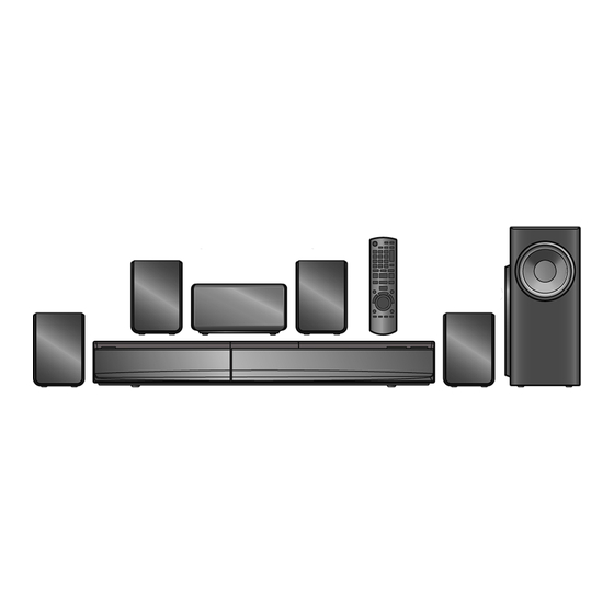
5.3. Speaker Connection------------------------------------- 15
5.4. Using the VIERA Link "HDAVI Control™"---------- 16
5.5. Using of iPod/iPhone------------------------------------ 18
5.6. Disc Information ------------------------------------------ 19
6 Self-Diagnosis and Special Mode Setting -------------- 21
6.1. Cold-Start -------------------------------------------------- 21
© Panasonic Corporation 2010. All rights reserved.
Unauthorized copying and distribution is a violation
of law.
SA-PT480EB
SA-PT480EG
(S)...Silver Type (EG)
PSG1002004CE
PAGE
Advertisement
Table of Contents
Troubleshooting

Related Manuals for Panasonic SA-PT480EB


Summary of Contents for Panasonic SA-PT480EB
-
Page 1: Table Of Contents
2.3. Service caution based on Legal restrictions -------- 8 6 Self-Diagnosis and Special Mode Setting -------------- 21 2.4. Handling Precautions for Traverse Unit-------------- 9 6.1. Cold-Start -------------------------------------------------- 21 © Panasonic Corporation 2010. All rights reserved. Unauthorized copying and distribution is a violation of law. - Page 2 6.2. Service Mode Table-------------------------------------- 21 11.11. SMPS P.C.B.---------------------------------------------- 92 6.3. Self-Diagnostic Mode ----------------------------------- 27 11.12. Power P.C.B.---------------------------------------------- 92 6.4. Self Diagnostic Function-Error Code ---------------- 28 11.13. Scart P.C.B. ----------------------------------------------- 93 6.5. Sales Demonstration Lock Function ---------------- 31 11.14. Waveform Table (1/3)----------------------------------- 94 6.6.
-
Page 3: Safety Precautions
1 Safety Precautions 1.1. GENERAL GUIDELINES 1. When servicing, observe the original lead dress. If a short circuit is found, replace all parts which have been overheated or damaged by the short circuit. 2. After servicing, see to it that all the protective devices such as insulation barriers, insulation papers shields are properly installed. -
Page 4: Protection Circuitry
1.3. Protection Circuitry The protection circuitry may have operated if either of the following conditions are noticed: • No sound is heard when the power is turned on. • Sound stops during a performance. The function of this circuitry is to prevent circuitry damage if, for example, the positive and negative speaker connection wires are “shorted”, or if speaker systems with an impedance less than the indicated rated impedance of the amplifier are used. -
Page 5: Caution For Ac Cord (For Eb Only)
1.5. Caution for AC Cord (For EB only) -
Page 6: Warning
2 Warning 2.1. Prevention of Electrostatic Discharge (ESD) to Electrostatic Sensitive (ES) Devices Some semiconductor (solid state) devices can be damaged easily by static electricity. Such components commonly are called Elec- trostatically Sensitive (ES) Devices. Examples of typical ES devices are integrated circuits and some field-effect transistors and semiconductor “chip”... -
Page 7: Precaution Of Laser Diode
2.2. Precaution of Laser Diode Caution: This product utilizes a laser diode with the unit turned “on”, invisible laser radiation is emitted from the pickup lens. Wavelength: 655 nm (DVD)/790 nm (CD) Maximum output radiation power from pickup: 100 W/VDE Laser radiation from the pickup unit is safety level, but be sure the followings: 1. -
Page 8: Service Caution Based On Legal Restrictions
2.3. Service caution based on Legal restrictions 2.3.1. General description about Lead Free Solder (PbF) The lead free solder has been used in the mounting process of all electrical components on the printed circuit boards used for this equipment in considering the globally environmental conservation. The normal solder is the alloy of tin (Sn) and lead (Pb). -
Page 9: Handling Precautions For Traverse Unit
2.4. Handling Precautions for Traverse Unit The laser diode in the optical pickup unit may break down due to static electricity of clothes or human body. Special care must be taken avoid caution to electrostatic breakdown when servicing and handling the laser diode in the traverse unit. Cautions to Be Taken in Handling the Optical Pickup Unit 2.4.1. - Page 10 2.4.2.2. Human body grounding 1. Use the anti-static wrist strap to discharge the static electricity form your body. Figure 2...
-
Page 11: Service Navigation
3 Service Navigation 3.1. Service Information This service manual contains technical information which will allow service personnel’s to understand and service this model. Please place orders using the parts list and not the drawing reference numbers. If the circuit is changed or modified, this information will be followed by supplement service manual to be filed with original service manual. -
Page 12: Specifications
250 W per channel (6 ), 1 kHz, 10% THD Plays DivX video. Subwoofer Ch: MPEG data recorded with Panasonic SD multi cameras or 250 W per channel (6 ), 100 Hz, 10% THD DVD video recoeders Comforming to SD VIDIO specification (ASF standard)/ Total RMS Dolby Digital mode power: MPEG4(Simple Profile)video system/G.726 audio system . -
Page 14: Location Of Controls And Components
5 Location of Controls and Components 5.1. Remote Control Key Button Operations... -
Page 15: Main Unit Key Button Operations
5.2. Main Unit Key Button Operations "SRD" lights when sound is output to the serround speakers. 5.3. Speaker Connection... -
Page 16: Using The Viera Link "Hdavi Control
5.4. Using the VIERA Link “HDAVI Control™”... -
Page 18: Using Of Ipod/Iphone
5.5. Using of iPod/iPhone... -
Page 19: Disc Information
5.6. Disc Information 5.6.1. Disc Playability (Media) - Page 20 5.6.2. File Extension Type Support (WMA/MP3/JPEG/MPEG4/DivX) DivX...
-
Page 21: Self-Diagnosis And Special Mode Setting
6 Self-Diagnosis and Special Mode Setting 6.1. Cold-Start Here is the procedure to carry out cold-start for initialize to shipping mode. 1. Unplug AC power cord 2. Press & hold [POWER] button 3. Plug AC power cord while [POWER] button being pressed FL Display will show “_ _ _ _ _ _ _ _”... - Page 22 6.2.1. Service Mode Table 1 (For DVD) Item Key Operation FL Display Mode Name Description Front Key Error code Error code check In STOP (no disc) mode, check The latest error code stored in the press [STOP] button on the EEPROM IC is displayed.
- Page 23 6.2.2. Service Mode Table 2 (For DVD) Item Key Operation FL Display Mode Name Description Front Key (Display 1) DVD laser DVD laser drive current measurement. In STOP (no disc) mode, drive current DVD laser drive current is measured press [STOP] button on the measurement and the result is displayed together main unit, and...
- Page 24 6.2.3. Service Mode Table 3 (For DVD) Item Key Operation FL Display Mode Name Description Front Key Micro-processor Micro-processor firmware version In STOP (no disc) (Display 1) firmware version display & EEPROM checksum display. mode, press [STOP] display & EEPROM checksum is only available button on the main unit, EEPROM due to existence of EEPROM IC.
- Page 25 6.2.4. Service Mode Table 4 (For DVD) Item Key Operation FL Display Mode Name Description Front Key (DVD) Main P.C.B. firmware version is In STOP (no disc) Main P.C.B. displayed on the FL Display. mode, press [STOP] firmware The firmware version can be updated button on the main unit, version display using recovery disc.
- Page 26 Product Region TV Broadcasting Model Series Country Region Signal System Region Display Code System OSD Menu Language Default (Default) (Default) USA, Canada, English (NA), Spanish (NA), P, PC, PX NTSC NTSC (*A) English US Militry Canadian, French Japan NTSC NTSC (*A) Japanese Japanese, English English (EU), French, German,...
-
Page 27: Self-Diagnostic Mode
6.3. Self-Diagnostic Mode Item Key Operation FL Display Mode Name Description Front Key Self-Diagnostic To enter into self-diagnostic checking Press & hold [STOP] on main Mode unit, follow by [4] then [9] on remote control. (When no disc in mechanism) Error code will display Error code System will perform a check on... -
Page 28: Self Diagnostic Function-Error Code
6.4. Self Diagnostic Function-Error Code 6.4.1. Mechanism Error Code Table Error Diagnosis Contents Description of error Automatic FL Display Remarks Code H01 Tray loading error The tray opening and closing is abnormal. Press [ STOP] on main CLOSE and OPEN of the tray cannot be unit for next error. - Page 29 6.4.2. DVD Module Error Code Table Error Diagnosis Contents Description of error Automatic FL Display Remarks Code U702 HDMI/DVI I2C The communication error of I2C when Press [ STOP] on main communication error connecting it with HDMI/DVI. For unit for next error. instance, when EDID information to which information on the TV set side has been described cannot be read, it is generated.
- Page 30 6.4.3. Power Supply & Digital Amplifier Error Code Table Error Diagnosis Contents Description of error Automatic FL Display Remarks Code F61 The abnormalities In normal operation, when DCDET2 goes Press [ STOP] on main in the D-Amp related to "L" (Low) (Not during POWER OFF unit for next error.
-
Page 31: Sales Demonstration Lock Function
6.5. Sales Demonstration Lock Function This function prevents discs from being lost when the unit is used for sales demonstrations by disabling the disc eject function. “LOCKED” is displayed on the unit, and ordinary operation is disabled. 6.5.1. Setting • Prohibiting removal of disc 1. -
Page 32: Firmware Version-Up Information
6.6. Firmware Version-Up Information 6.6.1. Process Flow (1/3) Item FL/ GUI Display Remarks Process Description Collect ROM There are 2 files: User can put both files Files into the same root A) Syscon ROM file type: (Copy files into Display 1: directory. -
Page 33: Process Flow
6.6.2. Process Flow (2/3) Item FL/ GUI Display Remarks Process Description GUI Display 1.3.2: GUI Display 1.3.2: UPDATING WRITING TO FLASHROM FL Display 2: Update stop Check Correct ROM files doesn’t fit to the (Wrong ROM Type) ROM file type product type. - Page 34 6.6.3. Process Flow (3/3) Item FL/ GUI Display Remarks Process Description 1. Update Failed Update software Update stop. FL Display 4: (Opecon) The theater set can’t work, If Opecon software update fail: and can’t be recovered by FL Display 3: "FAIL" . CD update again.
-
Page 35: Troubleshooting Guide
7 Troubleshooting Guide 7.1. Troubleshooting Guide for F61 and/or F76 This section illustrates the checking procedures when upon detecting the error of “F61” and/or “F76” after power up of the unit. It is for purpose of troubleshooting and checking in SMPS P.C.B. -
Page 36: Part Location
7.2. Part Location Photocouple: Switching IC: IC5799 PC5702, D5799 FUSE: F1 Rectifier: D5802 Switching IC: IC5701 Transformer: T5701 Figure 1. SMPS P.C.B. -
Page 37: Basic Troubleshooting Guide For Traverse Unit (Main P.c.b.)
7.3. Basic Troubleshooting Guide for Traverse Unit (Main P.C.B.) Problems Checking Points Checking components 1) Distorted picture or a) Check SDRAM address, data IC8051 abnormal sound is head bus, CLK and other control signals during the initialization waveform b) Check video signals (Y,C) LB8315, R8321, R8323, LB8316, R8325, R8327... -
Page 38: Basic Troubleshooting Guide For Hdmi Av Output
7.4. Basic Troubleshooting Guide for HDMI AV output Problems Checking Points Checking components 1) TV does not have any 1) Check setting of the set in * This year HDMI always ON. display. Set FL display Setup Menu whether the HDMI No need check Setup Menu. - Page 39 Problems Checking Points Checking components 1) TV does not have any 13) Hot-Plug Signal LB3906, R3902, R3903, Q3901, D3901 display. Set FL display shows U702/U703 14) TDMS Output swing amplitude R3901 control resistor 15) Host Interface External Input LB8702 Clock from LSI (IC8001) to Up-Con IC (IC3901) - OSC27M 16) Video Data Lines from LSI RX3707, RX3708, IC3901...
-
Page 40: Disassembly And Assembly Instructions
8 Disassembly and Assembly Instructions Caution Note: • This section describes the disassembly and/or assembly procedures for all major printed circuit boards & main compo- nents for the unit. (You may refer to the section of “Main components and P.C.B Locations” as described in the service manual) •... -
Page 41: Disassembly Flow Chart
8.1. Disassembly Flow Chart 8.3. Top Cabinet 8.7. Front Panel 8.6. DVD Mechanism Unit 8.4. AC Inlet P.C.B. Block Assembly (DLS6E) 8.8. FL P.C.B. 8.19. Power P.C.B. 8.5. Rear Panel 8.9. Power Button 8.20. SMPS P.C.B. P.C.B. 8.16. Main P.C.B. 8.21. -
Page 42: Main Components And P.c.b. Locations
8.2. Main Components and P.C.B. Locations... -
Page 43: Disassembly Of Top Cabinet
8.3. Disassembly of Top Cabinet Step 1 Remove 2 screws. Step 2 Remove 3 screws. Step 5 Press down the catches one by one. Caution: To avoid shocked by electricity & injured by high temperature. DO NOT TOUCH electrical components when insert hand under the Top Cabinet. -
Page 44: Disassembly Of Ac Inlet P.c.b
Caution: During assembling, ensure that catches of Top Step 3 Release Red (TL10) & Black (TL20) wires from the Wire Cabinet is insert into Front Panel properly. Holder. Caution: During assembling, ensure that Red (TL10) & Black (TL20) wires are dressed into Wire Holder. Step 4 Lift up AC Inlet P.C.B. -
Page 45: Disassembly Of Dvd Mechanism Unit (Dls6E)
8.6. Disassembly of DVD Mecha- nism Unit (DLS6E) Step 3 Remove 8 screws. • Refer to “Disassembly of Top Cabinet” Step 1 Detach 7P FFC at the connector (FP8251) on Main P.C.B.. Step 2 Detach 24P PFC at the connector (FP8531) on Main P.C.B.. -
Page 46: Disassembly Of Front Panel Block Assembly
Caution: During assembling, ensure that DVD Mechanism Unit (DLS6E) is properly located and fully seated on Bot- tom Chassis before screwing. Step 6 Attach a short pin to the 24P FPC of the DVD Mecha- nism Unit (DLS6E). Step 3 Fix 2 screws. Step 4 Attach 7P FFC at the connector (FP8251) on Main P.C.B.. -
Page 47: Disassembly Of Fl P.c.b
Caution: Do not exert strong force when releasing the tabs. Step 3 Detach 5P wire at the connector (FP9001) on Main P.C.B.. Step 6 Detach the Front Panel Block Assembly. Step 4 Release the 2 tabs at each side of the Front Panel Block Assembly in the direction of arrow. - Page 48 • Assembly of FL P.C.B. Step 1 Solder 4P cable to the connector (CN6001) on FL P.C.B.. Step 2 Release 1 catch. Step 3 Lift up FL P.C.B.. Step 2 Place FL P.C.B. onto Front Panel. Caution: Ensure that it is properly located & fully catched. Step 3 Dress 22P FFC according to diagram shown.
-
Page 49: Disassembly Of Power Button P.c.b
8.9. Disassembly of Power Button P.C.B. Step 4 Dress 4P cable into Front Panel’s ribs according to dia- • Refer to “Disassembly of Front Panel Block Assembly” gram shown. Step 1 Remove 1 screw. Step 2 Lift up Power Button P.C.B.. Step 5 Fix 5 screws to FL P.C.B.. - Page 50 Caution: Ensure that it is properly located & fully catched. Step 3 Desolder 4P Cable (H6803) on Power Button P.C.B.. Step 4 Remove Power Button P.C.B.. Step 3 Fix 1 screw onto Power Button P.C.B.. • Assembly of Power Button P.C.B. Step 4 Dress 4P cable flatly against the Top Wall of Front Step 1 Solder 4P cable at (H6803) onto Power Button P.C.B..
-
Page 51: Replacement Of Cradle Lid
8.10. Replacement of Cradle Lid • Refer to “Disassembly of Front Panel Block Assembly” 8.10.1. Disassembly of Cradle Lid Step 1 Release the Cradle Lid Spring by using a Flat head Screwdriver in the direction of arrow. Step 5 Dress 4P cable into Front Panel’s U-Slot & Ribs accord- ing to diagram shown. - Page 52 Step 4 Rotate the Cradle Lid about 45 according to the dia- Step 2 Slightly push the Cradle Lid inwards. gram shown. Step 3 Press the Cradle Lid downward. Step 5 Remove Cradle Lid. 8.10.2. Assembly of Cradle Lid Step 1 Insert the Cradle Lid (Shaft A) into the Front Panel (Slot A &...
-
Page 53: Disassembly Of Ipod Cradle Assembly
Step 5 Lift up iPod Cradle Assembly on both side. 8.11. Disassembly of iPod Cradle Assembly • Refer to “Disassembly of Front Panel Block Assembly” Step 1 Detach 15P FFC at the connector (CN1002) on iPod/ iPhone P.C.B.. Step 2 Remove 1 screw. Step 6 Press to release iPod Cradle Assembly from Front Panel as arrow shown. - Page 54 Step 2 Press the iPod Cradle Assembly downwards. Note: A “click” sound can be heard when the iPod Cradle Assembly is fixed onto Front Panel properly. Step 7 Remove iPod Cradle Assembly. Step 3 Press the catch on the iPod Cradle Assembly. Step 4 Fix 1 screw.
-
Page 55: Disassembly Of Ipod/Iphone P.c.b
Caution: During assembling, ensure that iPod/iPhone P.C.B. is seated properly at the locators. 8.13. Disassembly of USB P.C.B. • Refer to “Disassembly of Front Panel Block Assembly” 8.12. Disassembly of iPod/iPhone Step 1 Remove 1 screw. P.C.B. Step 2 Remove USB Support P.C.B.. •... -
Page 56: Replacement Of Dvd Lid Unit
8.14. Replacement of DVD Lid Unit • Refer to “Disassembly of Front Panel Block Assembly” 8.14.1. Disassembly of DVD Lid Unit Step 1 Push backward the Shaft B of the DVD Lid Unit in the direction of arrow. Step 2 Push forward the Shaft B of the DVD Lid Unit in the direction of arrow. - Page 57 8.14.2. Assembly of DVD Lid Unit Step 1 Insert the DVD Lid Unit into the Front Panel as arrow shown. Caution: Ensure that Shaft A of DVD Lid Unit is fully inserted into Slot A of Front Panel. Step 3 Insert the DVD Lid Unit (Shaft B) into the Front Panel (Slot B) as arrow shown.
-
Page 58: Disassembly Of Front Shield Plate
Caution: Ensure that the Shaft B of DVD Lid Unit is fully inserted into Shaft B of Front Panel. Step 3 Slightly lift up Front Shield Plate to release 2 catches at both side. Step 4 Remove Front Shield Plate unit. 8.15. -
Page 59: Disassembly Of Main P.c.b
Caution: During assembly, ensure that Front Shield Plate is properly located & fully catched onto Bottom Chassis. Step 9 Detach 10P wire at the connector (FP9001) on Main P.C.B.. 8.16. Disassembly of Main P.C.B. • Refer to “Disassembly of Top Cabinet” Step 1 Detach 18P FFC at the connector (CN2006) on Main P.C.B.. - Page 60 Step 14 Remove the Main P.C.B.. Step 11 Remove 6 screws. Step 12 Release the tab of the right side of the Rear Panel in Caution: During assembling, ensure that Main P.C.B. is the direction of arrow. seated properly at the locators. Step 13 Lift up to remove Main P.C.B.
-
Page 61: Disassembly Of D-Amp P.c.b
8.17. Disassembly of D-Amp P.C.B. • Refer to “Disassembly of AC Inlet P.C.B.” Step 1 Lift up 2 Wire Clampers. Step 2 Detach 3P Wire at the connector (CN5401) on D-Amp P.C.B.. Step 3 Detach 6P Cable at the connector (CN5400) on D-Amp P.C.B.. -
Page 62: Replacement Of Digital Amplifier Ic (Ic5100/ Ic5200)
8.18. Replacement of Digital Ampli- fier IC (IC5100/IC5200) • Refer to “Disassembly of D-Amp P.C.B.” 8.18.1. Disassembly of Digital Amplifier IC (IC5100/IC5200) Step 1 Place the D-Amp P.C.B. on an insulated material. Step 2 Remove 3 screws on Solder side of D-Amp P.C.B.. 8.18.2. -
Page 63: Disassembly Of Power P.c.b
Caution: During assembling, ensure that heatsink spacers Caution: During assembling, ensure that Power P.C.B. is is seated properly onto D-Amp Heatsink. properly attached & fully connected to SMPS P.C.B.. Step 5 Fix 3 screws. Caution: During assembling, ensure that screwing sequence is strictly follow to the illustration shown. - Page 64 Caution: Do not exert strong force when releasing the tabs. Step 3 Detach the Front Panel slightly forward. Step 7 Remove 5 screws on SMPS P.C.B.. Step 4 Lift up the Wire Clampers. Step 5 Detach 6P Cable wire at the connector (CN5400) on D- Amp P.C.B..
-
Page 65: Replacement Of Switching Regulator Ic (Ic5701)
Caution: During releasing P.C.B. Spacer, avoid touching the transformer & surrounding parts as it may lead to elec- tric shock or injuries due to high temperature. 8.21. Replacement of Switching Reg- ulator IC (IC5701) • Refer to “Disassembly of SMPS P.C.B.” Step 9 Lift up SMPS P.C.B. -
Page 66: Replacement Of Rectifier Diode (D5702)
(IC5701). Caution: Ensure pins of the Switching Regulator IC (IC5701) are properly seated and soldered on SMPS P.C.B.. Step 3 Remove the Switching Regulator IC (IC5701). Caution: Avoid touching the Heatsink Unit B due to its high temperature after prolonged use. Touching it may lead to injuries. - Page 67 8.22.2. Assembly Rectifier Diode (D5702) Step 1 Apply grease to the Heatsink Unit B. Step 2 Fix and screw the Rectifier Diode (D5702) to the Heat- sink Unit B. Caution: Ensure the Rectifier Diode (D5702) is tightly screwed to the Heatsink Unit B. Step 3 Mount the Heatsink Unit B with Rectifier Diode (D5702) onto SMPS P.C.B..
-
Page 68: Replacement Of Regulator Diode (D5802)
Caution: Ensure pins of the Rectifier Diode (D5702) are properly seated before soldered onto SMPS P.C.B.. Step 2 Remove 1 screw from the Regulator Diode (D5802). Step 3 Remove the Regulator Diode (D5802) from the SMPS P.C.B.. Caution: Avoid touching the Heatsink Unit A due to its high temperature after prolonged use. -
Page 69: Replacement Of Regulator Diode (D5803)
Caution: Ensure the Regulator Diode (D5802) is tightly screwed to the Heatsink Unit A. Step 4 Solder pins of the Regulator Diode (D5802) on the sol- der side of SMPS P.C.B.. Caution: Ensure pins of the Regulator Diode (D5802) are properly seated and soldered on SMPS P.C.B.. -
Page 70: Disassembly Of Scart P.c.b
Caution: Ensure the Regulator Diode (D5803) is tightly screwed to the Heatsink Unit A. Step 2 Detach 28P FFC at the connector (CN4001) on Scart P.C.B.. Step 3 Remove the Scart P.C.B. as arrow (1) and (2) shown. Caution: During assembling, ensure that Scart P.C.B. is properly inserted &... - Page 71 Caution: During assembling, ensure Fan Unit is properly located & fully catched onto Rear Panel. Step 3 Remove 2 screws. Step 4 Remove Fan Unit. Step 5 Remove 2 screws. Step 6 Lift up to remove Fan.
- Page 72 Caution: During assembling, ensure that 3P Wire is posi- tioned as diagram shown.
-
Page 73: Assembling And Disassembling Of Traverse Unit
9 Assembling and Disas- sembling of Traverse Unit 9.1. Disassembly of Traverse Unit • Follow (Step 1) to (Step 6) of Item 8.3 • Follow (Step 1) to (Step 5) of Item 8.6 Step 1 Release the guide and slide the traverse slide plate (rib) as arrows shown. - Page 74 Step 4 Release the guide and slide the traverse slide plate (rib) in the direction of arrows shown to lock in the traverse unit. Step 2 Slot the traverse unit approximately 45 into the mecha chassis as arrow shown. Note: Ensure the bosses fix exactly onto the guides. Step 3 Place down the traverse unit as arrow shown.
-
Page 75: Service Position
10 Service Position Note: For description of the disassembly procedures, see the Section 8. 10.1. Checking & Repairing Main P.C.B. 10.1.1. Checking & Repairing of Side B of Main P.C.B. Step 1 Remove Top Cabinet. Step 2 Detach 18P FFC at the connector (CN2006) on Main P.C.B.. - Page 76 Step 14 Lift up to remove Main P.C.B. Shield Plate. 10.1.2. Checking & Repairing of Side A of Main P.C.B. Step 1 Detach 28P FFC at the connector (CN2009) on Main P.C.B.. Step 15 Connect 18P FFC to the connector (CN2006) on Main P.C.B..
-
Page 77: Checking & Repairing D-Amp P.c.b
Step 5 Lift up the Main P.C.B.. Step 6 Flip the Main P.C.B. according to diagram shown. 10.2. Checking & Repairing D-Amp P.C.B. 10.2.1. Checking & Repairing of Side B of D-Amp P.C.B. Step 1 Remove Top Cabinet. Step 2 Remove D-Amp P.C.B.. Step 3 Remove D-Amp Heatsink. - Page 78 Step 4 Twist the Wire Clamper to release 6P Cable. Step 5 Remove 2 screws. Step 9 Twist the Wire Holder. Step 10 Release Red (TL10) & Black (TL20) wires from the Wire Holder. Step 11 Remove AC Inlet P.C.B.. Step 6 Remove 6 screws.
-
Page 79: Checking & Repairing Smps P.c.b
Step 4 Slightly move Front Panel Block Assembly forward according to diagram shown. 10.3. Checking & Repairing SMPS P.C.B. Step 1 Remove Top Cabinet. Step 2 Release the 3 tabs at the Bottom Chassis. Step 5 Remove 1 screw. Step 6 Twist the Wire Holder. Step 3 Release the 2 tabs at each side of the Front Panel Block Step 7 Release Red (TL10) &... - Page 80 Caution: During releasing P.C.B. Spacer, ensure that long nose plier avoid touching the electrical components. Step 11 Release P.C.B. Spacer by using long nose plier. Step 9 Twist the Wire Clampers to release 6P (SMPS P.C.B. to D-Amp P.C.B.) & 10P (SMPS P.C.B. to Main P.C.B.) cables. Step 12 Flip the SMPS P.C.B.
-
Page 81: Checking & Repairing Fl P.c.b
Step 6 Remove 1 screw. 10.4. Checking & Repairing FL P.C.B. Step 1 Remove Top Cabinet. Step 2 Remove Front Panel Block Assembly. Step 3 Remove 5 screws. Step 7 Lift up Power Button P.C.B.. Step 4 Release 1 catch on FL P.C.B.. Step 8 Connect 22P FFC to the connector (CN2002) on Main P.C.B.. -
Page 83: Voltage & Waveform Chart
CD PLAY STANDBY IC2300 REF NO. MODE CD PLAY STANDBY IC2300 REF NO. MODE CD PLAY STANDBY IC2300 REF NO. MODE CD PLAY STANDBY IC2300 REF NO. MODE CD PLAY STANDBY REF NO. IC2300 MODE CD PLAY STANDBY SA-PT480EB/EG MAIN P.C.B. -
Page 84: Main P.c.b. (2/7)
CD PLAY STANDBY IC2800 REF NO. MODE CD PLAY -6.6 STANDBY -6.8 IC2801 REF NO. MODE CD PLAY -7.0 STANDBY -7.0 IC2802 REF NO. MODE CD PLAY -7.0 STANDBY -7.0 IC2952 REF NO. MODE CD PLAY STANDBY SA-PT480EB/EG MAIN P.C.B. -
Page 85: Main P.c.b. (3/7)
CD PLAY STANDBY IC3901 REF NO. MODE CD PLAY STANDBY IC3901 REF NO. MODE CD PLAY STANDBY IC3952 REF NO. MODE CD PLAY STANDBY IC3953 REF NO. MODE CD PLAY STANDBY REF NO. IC8001 MODE CD PLAY STANDBY SA-PT480EB/EG MAIN P.C.B. -
Page 86: Main P.c.b. (4/7)
CD PLAY STANDBY IC8001 REF NO. MODE CD PLAY STANDBY IC8001 REF NO. MODE CD PLAY STANDBY IC8001 REF NO. MODE CD PLAY STANDBY IC8001 REF NO. MODE CD PLAY STANDBY IC8001 REF NO. MODE CD PLAY STANDBY SA-PT480EB/EG MAIN P.C.B. -
Page 87: Main P.c.b. (5/7)
CD PLAY STANDBY REF NO. IC8251 MODE CD PLAY STANDBY IC8422 REF NO. MODE CD PLAY STANDBY IC8601 REF NO. MODE CD PLAY STANDBY IC8606 REF NO. MODE CD PLAY STANDBY IC8611 REF NO. MODE CD PLAY STANDBY SA-PT480EB/EG MAIN P.C.B. -
Page 88: Main P.c.b. (6/7)
REF NO. MODE CD PLAY STANDBY IC9002 REF NO. MODE CD PLAY STANDBY IC9003 REF NO. MODE CD PLAY STANDBY REF NO. IC9006 MODE CD PLAY STANDBY Q2301 Q2302 Q2303 Q2304 Q2400 REF NO. MODE CD PLAY STANDBY SA-PT480EB/EG MAIN P.C.B. -
Page 89: Main P.c.b. (7/7)
Q8552 Q8561 REF NO. MODE CD PLAY STANDBY Q8562 Q8563 Q8564 Q8565 QR2400 REF NO. MODE CD PLAY STANDBY QR2605 QR2606 QR2700 QR2701 QR8420 REF NO. MODE CD PLAY STANDBY QR9030 REF NO. MODE CD PLAY STANDBY SA-PT480EB/EG MAIN P.C.B. -
Page 90: Fl P.c.b
-21.2 -23.4 -21.2 -14.8 -14.8 -21.2 -23.4 -14.8 -12.6 -23.9 -17.1 -23.6 -21.4 -21.4 -21.4 -21.4 -21.4 -21.4 -21.4 -21.4 REF NO. IC6001 MODE CD PLAY -21.4 -21.4 STANDBY -21.4 -21.4 Q6100 Q6800 REF NO. MODE CD PLAY STANDBY SA-PT480EB/EG FL P.C.B. -
Page 91: D-Amp P.c.b. (1/2)
CD PLAY STANDBY IC5400 REF NO. MODE CD PLAY 13.1 18.0 11.6 STANDBY 13.1 18.0 11.6 IC5401 REF NO. MODE CD PLAY STANDBY IC5402 REF NO. MODE CD PLAY STANDBY IC5404 REF NO. MODE CD PLAY STANDBY SA-PT480EB/EG D-AMP P.C.B. -
Page 92: D-Amp P.c.b. (2/2)
Q5414 QR5400 QR5401 REF NO. MODE CD PLAY 12.0 STANDBY 12.0 SA-PT480EB/EG D-AMP P.C.B. 11.11. SMPS P.C.B. IC5701 REF NO. MODE CD PLAY 19.5 -11.6 -11.6 -8.1 -11.6 -11.3 -11.5 STANDBY 19.5 -11.6 -11.6 -8.1 -11.6 -11.3 -11.5 REF NO. -
Page 93: Scart P.c.b
11.13. Scart P.C.B. REF NO. IC4001 MODE CD PLAY STANDBY IC4001 REF NO. MODE CD PLAY STANDBY Q4002 Q4003 Q4004 REF NO. MODE CD PLAY STANDBY SA-PT480EB/EG SCART P.C.B. -
Page 94: Waveform Table (1/3)
11.14. Waveform Table (1/3) 4Vp-p(2usec/div) 5Vp-p(500nsec/div) 3Vp-p(20usec/div) 3.4Vp-p(100nsec/div) 1.5Vp-p(100nsec/div) 0.1Vp-p(200usec/div) 0.15Vp-p(500usec/div) 0.1Vp-p(100usec/div) 1.5Vp-p(500usec/div) 0.1Vp-p(200usec/div) 0.6Vp-p(10usec/div) 0.1Vp-p(100usec/div) 3.6Vp-p(5usec/div) 3.8Vp-p(5usec/div) 3.8Vp-p(5usec/div) 3.6Vp-p(5usec/div) 3.6Vp-p(2usec/div) 3.6Vp-p(5usec/div) 3.8Vp-p(5usec/div) 3.8Vp-p(5usec/div) -
Page 95: Waveform Table (2/3)
11.15. Waveform Table (2/3) 0.68Vp-p(10usec/div) 1Vp-p(20usec/div) 0.6Vp-p(20usec/div) 0.48Vp-p(20usec/div) 80Vp-p(1usec/div) 3.8Vp-p(5msec/div) 2Vp-p(20usec/div) 5.2Vp-p(1usec/div) 5.6Vp-p(1usec/div) 6.8Vp-p(1usec/div) 76Vp-p(1usec/div) 3.6Vp-p(500nsec/div) 6Vp-p(1usec/div) 5.6Vp-p(1usec/div) 7.2Vp-p(1usec/div) 1.5Vp-p(2usec/div) 3.2Vp-p(2usec/div) 6Vp-p(5usec/div) 6Vp-p(5usec/div) 6Vp-p(5usec/div) -
Page 96: Waveform Table (3/3)
11.16. Waveform Table (3/3) 6Vp-p(5usec/div) 6Vp-p(5usec/div) 6Vp-p(5usec/div) 6Vp-p(5usec/div) 0.58Vp-p(20usec/div) 6Vp-p(5usec/div) 2Vp-p(2usec/div) 6Vp-p(1usec/div) 0.52Vp-p(20usec/div) 1.6Vp-p(20usec/div) 0.64Vp-p(20usec/div) 6Vp-p(2usec/div) 1.5Vp-p(500usec/div) 3.8Vp-p(1usec/div) 6Vp-p(2usec/div) 0.15Vp-p(500usec/div) 1.4Vp-p(20nsec/div) -
Page 97: Illustration Of Ics, Transistor And Diode
12 Illustration of ICs, Transistor and Diode C0HBB0000057 (44P) RFKWMPT480EB MFI341S2164 (20P) C0DBZYY00018 (8P) C0JBAZ001251 (20P) MN864702A (128P) (100P) C1AB00003205 (16P) C3EBFY000006 (8P) C0DBAYY00729 (20P) MN2DS0018MP No.1 C0ABBB000189 (8P) C1AB00002461 (38P) (216P) C0ABBB000179 (8P) RFKWMH52B3D1 (48P) C0FBAK000026 (16P) C1AB00003260 (36P) REPX0829A (8P)(EG) C0JBAR000540 (16P) C3ABPG000160 (54P) -
Page 99: Overall Simplified Block Diagram
13 Overall Simplified Block Diagram AUDIO VIDEO SCART WIRELESS DIGITAL Power Supply PY/PR/PB/Y DAMP SELECTOR SPEAKERS D-AMP RGB/Y TUNER VIDEO Buffer TUNER iPOD B/E+MAIN Processor DVD MECHANISM SMPS DV5 LSI DC_DC HDMI Main Trans Backup Trans Relay HDMI iPod/ iPhone A.S.S. -
Page 100: Block Diagram
105 LPC2 SP DRV VIN3 LEVEL DRV1 66 SPINDLE SHIFTER MOTOR VO3- FP8251 TRAVERSE UNIT OPIN- OPOUT AD1 122 OPIN+ ACTUATOR FP8531 VO1+ TRACKING COIL LEVEL SHIFTER FP8531 VO1- FP8531 VO2+ FOCUS COIL LEVEL SHIFTER FP8531 VO2- SA-PT480EB/EG MAIN(SERVO) BLOCK DIAGRAM... -
Page 101: Main(System Control)
CN2007 CN1002 CN1001 iPod DET 74 Q2601 UART TX CN2007 CN1002 CN1001 UART TX 35 SWITCH QR2605 PCONT SWITCH Q2602 CN2007 CN1002 CN1001 UART RX UART RX 36 SWITCH QR2606 PCONT SWITCH PCONT PCONT 50 SA-PT480EB/EG MAIN(SYSTEM CONTROL) BLOCK DIAGRAM... -
Page 102: Main(Up-Con)
NRST NRST 70 1 IN1 TXRST NRESET HDMIRST TRCDATATA2 79 2 IN2 IC8606 C0EBE0000456 RESET HOTPLG FG 71 Q3904 FROM/TO CEC IN OUT SWITCH CEC IO 13 CEC MAIN(SYSTEM CONTROL) IC3953 C0JBAB000986 INVERTER 14 ARC MAIN(AUDIO) SA-PT480EB/EG MAIN(UP-CON) BLOCK DIAGRAM... -
Page 103: Main(Audio)
DIGITAL AUDIO IECINPUT OPT-IN 3 EXTRG1 Q2800 IN OPTICAL SEL A SEL A SWITCH 10 A (LSB) FROM MAIN(SYSTEM CONTROL) Q2805 SEL B SEL B SWITCH 9 B (MSB) FROM 191 DQM2 MAIN(UP-CON) DMIXOUT ADOUT 151 SA-PT480EB/EG MAIN(AUDIO) (1/2) BLOCK DIAGRAM... - Page 104 AUDIO DATA DELTA-SIGMA 4 LRCK INTERFACE INTERPOLATOR MODULATOR 3 SDTI AOUTR RECOUT R RECOUT-R CN2009 CN4001 FROM DAC MUTE 6 SMUTE CONTROL MAIN(SYSTEM CONTROL) PORT Q2554 Q2301 MUTING FROM MUTING SCART MUTE CONTROL MAIN(SYSTEM CONTROL) SA-PT480EB/EG MAIN(AUDIO) (2/2) BLOCK DIAGRAM...
-
Page 105: Main(Video)
CN2009 CN4001 DAC3OUT BUFFER FP8531 VIN2 97 VIN1RF SCART P.C.B. 116 VIN8 FP8531 VIN3 99 VIN4RF 113 VIN5 FP8531 VIN4 VIN3RF 114 VIN6 FP8531 VIN9 112 VIN9 FP8531 VIN10 111 VIN10 FP8531 96 RFINP TRAVERSE UNIT SA-PT480EB/EG MAIN(VIDEO) BLOCK DIAGRAM... -
Page 106: Digital Audio
CN5402 DCDET DC DETECT DC DETECT Q5408, Q5409, Q5414 Q5400,Q5401,Q5402, Q5403,Q5404,Q5405 FAN DC OUT CN5401 FAN CONTROL CIRCUIT CN5401 FAN LOCK FROM/TO MAIN(SYSTEM CONTROL) QR5401 DC DETECT CN2006 CN5402 ECO CIRCUIT FROM DCDET POWER SUPPLY SA-PT480EB/EG DIGITAL AUDIO BLOCK DIAGRAM... -
Page 107: Analog Video
CRSAG CN2009 CN4001 YC H 28 SEL3 Q4002 CN2009 CN4001 VMUTE MUTING 5 MUTE1 CONTROL 14 MUTE2 FROM MAIN(SYSTEM CONTROL) Q4003 Q4004 CN2009 CN4001 RGB H BUFFER BLANKING I/O CN2009 CN4001 FUN SW FUNCTION SW SA-PT480EB/EG ANALOG VIDEO BLOCK DIAGRAM... -
Page 108: Power Supply
D5405 CN5400 +51V +55V PVDD TO POWER SUPPLY D5407 SECTION (2/2) DCDET DIGITAL AUDIO PC5720 D-AMP P.C.B. FEED BACK FROM FEED BACK POWER CONT JW2* CN2004 CIRCUIT MAIN(SYSTEM CONTROL) IC5801 C0DABFC00002 SHUNT REGULATOR Q5863 COLD SA-PT480EB/EG POWER SUPPLY(1/2) BLOCK DIAGRAM... - Page 109 CN1002 CN1001 DETECT MAIN(SYSTEM CONTROL) Q2604 IC2602 C0DBZYY00311 CN2007 CN1002 CN1001 HIGH SIDE iPod CTRL SW SWITCH SWITCH CN2007 CN1002 CN1001 1 IN VOUT 5 BATTPCONT 3 EN OC 4 FROM/TO MAIN(SYSTEM CONTROL) iPod OC SA-PT480EB/EG POWER SUPPLY(2/2) BLOCK DIAGRAM...
-
Page 110: Wiring Diagram
AC INLET P.C.B. SPEAKERS (SOLDER SIDE) (SOLDER SIDE) (SOLDER SIDE) USB PORT CENTER P5701 SCART P.C.B. H6803 (SOLDER SIDE) SUBWOOFER CN6402 AC IN 220V-240V 50Hz CN6401 TL10* TL20* JK4001 NOTE: " * " REF IS FOR INDICATION ONLY. SA-PT480EB/EG WIRING CONNECTION... -
Page 111: Schematic Diagram Notes
16 Schematic Diagram Notes • Voltage and signal line : +B signal line • This schematic diagram may be modified at any time : -B signal line with the development of new technology. : Audio output signal line Notes: : Video output signal line S6002: Stop switch ( : CD/DVD Audio input signal line... -
Page 113: Schematic Diagram
SECTION (2/6) VDD12 C8529 C8528 C8201 C8501 6.3V100 6.3V100 SBT3 DV: MAIN(DV5U): SCHEMATIC DIAGRAM - 1 ~ 6 HD: MAIN(HDMI): SCHEMATIC DIAGRAM - 7 AIN0 MA: MAIN(MICON): SCHEMATIC DIAGRAM - 8 ~ 13 C8505 TO MAIN(DV5U) SECTION (4/6) SA-PT480EB/EG MAIN(DV5U) CIRCUIT... - Page 114 SWITCH K8004 ...EG TO MAIN(DV5U) SECTION (3/6) DV: MAIN(DV5U): SCHEMATIC DIAGRAM - 1 ~ 6 TO MAIN(DV5U) HD: MAIN(HDMI): SCHEMATIC DIAGRAM - 7 SECTION (1/6) MA: MAIN(MICON): SCHEMATIC DIAGRAM - 8 ~ 13 TO MAIN(DV5U) SECTION (5/6) SA-PT480EB/EG MAIN(DV5U) CIRCUIT...
- Page 115 LB8691 CKDOP_CPUCLK MA CPU-CMD LB8693 CKDOP_CPUCMD MA CPU-STAT LB8692 CKDOPCPUSTAT MA DV: MAIN(DV5U): SCHEMATIC DIAGRAM - 1 ~ 6 HD: MAIN(HDMI): SCHEMATIC DIAGRAM - 7 MA: MAIN(MICON): SCHEMATIC DIAGRAM - 8 ~ 13 TO MAIN(DV5U) SECTION (6/6) SA-PT480EB/EG MAIN(DV5U) CIRCUIT...
- Page 116 C8652 FEXDT_9 EXADR9_DT11 FEXDT_13 FEXDT_14 FEXDT_8 EXADR8_DT4 XBYTE C9003 FEXDT_15 EXADR_16 IC8651 RFKWMH52B3D1 FLASH MEMORY DV: MAIN(DV5U): SCHEMATIC DIAGRAM - 1 ~ 6 HD: MAIN(HDMI): SCHEMATIC DIAGRAM - 7 MA: MAIN(MICON): SCHEMATIC DIAGRAM - 8 ~ 13 SA-PT480EB/EG MAIN(DV5U) CIRCUIT...
- Page 117 DV: MAIN(DV5U): SCHEMATIC DIAGRAM - 1 ~ 6 AUDIODIGITAL D1H88204A043 AUDIODIGITAL HD: MAIN(HDMI): SCHEMATIC DIAGRAM - 7 I2C_SDA I2C_SDA C8051 MA: MAIN(MICON): SCHEMATIC DIAGRAM - 8 ~ 13 RX8018 I2C_SCL I2C_SCL D1H422020001 HOTPLG NCAS NCAS HOTPLG CKGV_CLK NRAS NRAS CKGVCLK LB8901 R8901 J0JCC0000308 SA-PT480EB/EG MAIN(DV5U) CIRCUIT...
- Page 118 VO1- VO1- VO4- VO1+ VO1+ VO4+ R8263 R8261 C8264 C8364 C8260 220P OPIN- OPIN+ K8252 DV: MAIN(DV5U): SCHEMATIC DIAGRAM - 1 ~ 6 HD: MAIN(HDMI): SCHEMATIC DIAGRAM - 7 MA: MAIN(MICON): SCHEMATIC DIAGRAM - 8 ~ 13 SA-PT480EB/EG MAIN(DV5U) CIRCUIT...
- Page 119 C0JBAB000986 LB3909 R3952 IC3952 INVERTER J0JHC0000045 C0CBCDC00063 TXRST TXRST R3958 VOLTAGE REGULATOR OSC27M OSC27M I2C_SCL I2C_SCL I2C_SDA I2C_SDA C3955 0.01 C3972 RX3901 R3956 D1H410120001 VCLK R3947 CKGVCLK HOTPLG HOTPLG K3903 C3967 C3970 R3900 M+9V 100K R3955 PW_M+9V SA-PT480EB/EG MAIN(HDMI) CIRCUIT...
- Page 120 R2815 B1GBCFJJ0051 PW_+7V R2816 SWITCH SEL_B Q2800 SEL_A B1GBCFJJ0051 SWITCH AGND DV: MAIN(DV5U): SCHEMATIC DIAGRAM - 1 ~ 6 HD: MAIN(HDMI): SCHEMATIC DIAGRAM - 7 MA: MAIN(MICON): SCHEMATIC DIAGRAM - 8 ~ 13 TO MAIN(MICON) SECTION (4/6) SA-PT480EB/EG MAIN(MICON) CIRCUIT...
- Page 121 DGND VSS2 MODE0 R2098 LB2091 J0JGC0000020 PW_+3.3V TO MAIN(MICON) SECTION (3/6) DV: MAIN(DV5U): SCHEMATIC DIAGRAM - 1 ~ 6 HD: MAIN(HDMI): SCHEMATIC DIAGRAM - 7 MA: MAIN(MICON): SCHEMATIC DIAGRAM - 8 ~ 13 TO MAIN(MICON) SECTION (5/6) SA-PT480EB/EG MAIN(MICON) CIRCUIT...
- Page 122 DV: MAIN(DV5U): SCHEMATIC DIAGRAM - 1 ~ 6 C2571 R2820 C2820 R2821 HD: MAIN(HDMI): SCHEMATIC DIAGRAM - 7 220P 220P AUXR MA: MAIN(MICON): SCHEMATIC DIAGRAM - 8 ~ 13 C2570 C2819 R2819 220P 220P R2818 TO MAIN(MICON) SECTION (6/6) AUXL SA-PT480EB/EG MAIN(MICON) CIRCUIT...
- Page 123 CY_IN 16V47 Y_PY_G_OUT iPod_VOUT CB_IN VGND VOUT CB_PB_B_OUT CR_IN CR_PR_R_OUT IC2601 C0ABZA000080 ISOLATION AMP iPod_DET DV: MAIN(DV5U): SCHEMATIC DIAGRAM - 1 ~ 6 HD: MAIN(HDMI): SCHEMATIC DIAGRAM - 7 MA: MAIN(MICON): SCHEMATIC DIAGRAM - 8 ~ 13 SA-PT480EB/EG MAIN(MICON) CIRCUIT...
- Page 124 B1GBCFJJ0051 R2709 B1ABCF000176 DC DETECT DC DETECT R2737 R2738 PW_-7V DV: MAIN(DV5U): SCHEMATIC DIAGRAM - 1 ~ 6 HD: MAIN(HDMI): SCHEMATIC DIAGRAM - 7 PGND MA: MAIN(MICON): SCHEMATIC DIAGRAM - 8 ~ 13 PW_SW+5V PW_+3.3V PW_+7V PW_+9V SA-PT480EB/EG MAIN(MICON) CIRCUIT...
- Page 125 DV: MAIN(DV5U): SCHEMATIC DIAGRAM - 1 ~ 6 HD: MAIN(HDMI): SCHEMATIC DIAGRAM - 7 iPhone_RST I2C_SCL nRESET MA: MAIN(MICON): SCHEMATIC DIAGRAM - 8 ~ 13 I2C_SDA PW_+3.3V MODE0 MODE1 R2402 IC2400 LB2400 TO MAIN(MICON) J0JGC0000021 MFI341S2164 SECTION (5/6) MICRO CONTROLLER SA-PT480EB/EG MAIN(MICON) CIRCUIT...
-
Page 126: Fl Circuit
VOL - DGND_ASS R6801 R6021 R6022 R6023 R6024 1.2K 1.5K 2.2K 3.3K 4.7K S6807 S6007 R6025 OPEN/CLOSE SELECTOR CN6001 L6007 J0JBC0000014 DGND POWER BUTTON KEY1 L6006 J0JBC0000014 KEY1_BTN CIRCUIT (H6803) L6005 IN SCHEMATIC LED_VREF LED_VREF DIAGRAM - 21 SA-PT480EB/EG FL CIRCUIT... -
Page 127: D-Amp Circuit
DAP_SCL_2 FRONT L - RESERVED DAP_LRCLK DAP_SCLK FRONT L + TO SPEAKERS LRCLK SCLK FRONT R - FRONT R + CENTER - CENTER + SUBWOOFER - SUBWOOFER + IC5405 C0JBAA000501 AND GATE VALID1 TO D-AMP SECTION (3/4) SA-PT480EB/EG D-AMP CIRCUIT... - Page 128 R5445 D5620 1000P SPK_GND 35V470 B0HCSP000001 D5512 B0ACCK000005 D5619 L5106 B0HCSP000001 G0B9R5K00005 R5136 100K C5156 C5143 R5125 R5452 1000P 35V330 R5135 5.6K 100K 5.6K C5142 C5157 C5144 1000P 35V470 D5618 D5510 B0HCSP000001 B0ACCK000005 TO D-AMP SECTION (4/4) SA-PT480EB/EG D-AMP CIRCUIT...
- Page 129 B0BC7R5A0268 C5437 C5418 R5438 16V22 6.3V100 220K R5428 D5404 R5424 R5435 Q5405 B0ACCK000005 Q5412 B1ABCF000011 B1ABCF000011 SWITCH R5437 R5427 D5403 C5423 R5423 C5417 D5402 B0ACCK000005 16V10 B0BC012A0269 4.7K DC DETECT 100K C5424 5600P TO D-AMP SECTION (4/4) SA-PT480EB/EG D-AMP CIRCUIT...
- Page 130 1000P C5204 C5231 0.01 C5237 C5228 R5215 R5220 1000P 0.47 100K R5214 D5611 B0HCSP000001 C5230 1000P C5238 C5232 1000P 0.01 PVDD D5610 B0HCSP000001 D5628 D5627 R5474 B0BC012A0269 B0ACCK000005 C5450 R5473 R5472 16V22 6.8K TO D-AMP SECTION (3/4) SA-PT480EB/EG D-AMP CIRCUIT...
-
Page 131: Smps Circuit
PCONT PCONT DC_18V R5805 DC18V 6.8K DC12V MAIN(MICON) PGND Q5863 CIRCUIT (CN2004) B1ABGC000001 R5819 IN SCHEMATIC R5728 DC5V SWITCH R5817 DIAGRAM - 12 DCDET 2.2K DCDET SYS5V SYS6V SYNC R5861 C5869 C5828 R5818 SYNC 6.3V2200 100K 0.01 SA-PT480EB/EG SMPS CIRCUIT... - Page 132 TO SMPS C5720 C5725 OLP/SS 1000P R5733 SECTION (1/2) D5705 B0BC020A0267 D5710 ZJ5702 B0EAMM000057 C5722 C5724 C5730 C5700 1000P R5732 D5713 F1BAF1020020 1000P B0BC030A0264 1000P C5721 C5726 D5708 C5747 220P 50V10 820P B0ACCK000005 R5726 R5727 0.27 0.27 SA-PT480EB/EG SMPS CIRCUIT...
-
Page 133: Power, Power Button & Ac Inlet Circuit
L6806 FL CIRCUIT DGND SMPS CIRCUIT L6804 KEY1_BTN AC IN (CN6001) L6805 IN SCHEMATIC 220V~240V 50Hz IN SCHEMATIC DIAGRAM - 20 L6803 LED VREF DIAGRAM - 14 TL20* D6800 (BLK) B3ABA0000187 SA-PT480EB/EG POWER / POWER BUTTON / AC INLET CIRCUIT... -
Page 134: Ipod/Iphone & Usb Circuit
L1029 R1011 IN - L DOCK_R OUT J0JFC0000006 L1030 IN - R iPod DET R1001 R1003 R1004 OUT_L L1032 VGND 100K 100K J0JBC0000015 R1002 OUT_R VIDEO AUDIO_RETURN VGND L1009 iPod_DET L1031 R1012 J0JFC0000006 L1008 J0JFC0000006 SA-PT480EB/EG iPod/iPhone / USB CIRCUIT... -
Page 135: Scart Circuit
CBIN CBSAG AGND C4005 C4011 R4202 C4008 A(B)IN 470P 680P 470P A(B)IN MUTE2 GND2 AGND C4041 A(B)OUT C4037 A(B)OUT 6.3V470 CR_IN CRIN CROUT C4010 Q4004 470P B1GDCFEJ0008 VCC2 CRSAG C4046 SWITCH CHASSIS RGB_H Q4003 B1GBCFLL0043 SWITCH YC_H SA-PT480EB/EG SCART CIRCUIT... -
Page 136: Printed Circuit Board
R8334 LB8314 R8565 R8555 C8320 Q8331 R8333 C8321 R8324 LB8315 R2402 R8323 C2400 Q8321 C2620 C2622 IC2400 C2623 L2951 R2964 C2951 Q2554 R2513 R2956 R2959 4 5 6 C2961 R2509 C2957 C2958 IC2952 0655A 0655A (SIDE A) SA-PT480EB/EG MAIN P.C.B. - Page 137 C8533 D2800 RX8532 R2819 LB8255 RX8533 R2818 C2819 L2705 C2711 1-GND 3-LCH R2516 C2900 L2900 FP8531 JK2951 FP8251 (TO OPTICAL PICKUP (TO TRAVERSE / UNIT) SPINDLE) R2951 C2959 C2960 R2952 FM ANT X2951 0655A 0655A (SIDE B) SA-PT480EB/EG MAIN P.C.B.
-
Page 138: Fl, Power, Power Button & Ac Inlet P.c.b
AC INLET P.C.B. (REPX0803A) 0653AD 0653AD P5701 L6806 D6800 H6803 S6801 (POWER) AC IN 220V-240V 50Hz TL10* TL20* 0662BC-1 0662BC-1 NOTE: " * " REF IS FOR INDICATION ONLY. SA-PT480EB/EG FL / POWER / POWER BUTTON / AC INLET P.C.B. -
Page 139: D-Amp P.c.b
D5612 D5621 L5106 5-FR+ D5619 4-C- CENTER L5203 3-C+ R5220 2-SW- R5223 SUBWOOFER D5610 C5237 D5613 R5219 D5616 1-SW+ L5204 0661AA 0661AA 0661AA 0661AA (SIDE A) (SIDE B) NOTE: " * " REF IS FOR INDICATION ONLY. SA-PT480EB/EG D-AMP P.C.B. -
Page 140: Smps P.c.b
CN5802 D5702 C5840 C5726 C5824 PC5720 Q5863 JW2* C5869 R5804 R5861 R5806 C5818 R5730 IC5801 C5800 D5707 ZJ5702 R5819 R5805 D5712 R5817 R5720 R5818 HEATSINK ZJ5703 0662BA-1 0662BA-1 NOTE: " * " REF IS FOR INDICATION ONLY. SA-PT480EB/EG SMPS P.C.B. -
Page 141: Ipod/Iphone, Usb & Scart P.c.b
W4036 C4037 CN6401 IC4001 C4013 C4041 C4040 C4044 R4006 W4045 R4003 R4002 R4001 R4007 L4004 L4003 L4002 L4001 R4104 R4204 C4009 C4007 C4004 C4003 C4002 C4001 R4005 C4010 C4008 C4006 0654A 0654A JK4001 SA-PT480EB/EG iPod/iPhone / USB / SCART P.C.B. -
Page 143: Terminal Function Of Ics
19 Terminal Function of ICs PCONT O System Power Control RGB_H O Blanking signal for SCART VMUTE2 O SCART Function Switch Control 19.1. IC2300 (RFKWMPT480EB): IC VMUTE I/O Video Mute Control YC_H O To Select Luminance or Com- MICROPROCESSOR posite Out SCART_MUTE O Mute control of SCART Audio UNLOAD_SW... -
Page 144: Ic6001 (C0Hbb0000057): Ic Fl Driver
19.2. IC6001 (C0HBB0000057): IC FL Driver Terminal Name Function LED1 LED2 LED3 LED4 Oscillator Input DOUT Data Output Data Input Clock Input Serial Interface Strobe Key Data Input 1 (No Connec- tion) Key Data Input 2 (No Connec- tion) Power Supply (+5V) O Segment Output 18 O Segment Output 17 O Segment Output 16... -
Page 145: Exploded View And Replacement Parts List
CN5802 *TL21 CN5803 ZJ5703 28-3 12-1 ZJ5702 12-1 28-1 28-1 CN1002 28-1 18-1 18-1 (iPod / iPhone P.C.B.) 28-1 28-2 CN1001 18-1 SA-PT480EB/EG-K, EG-S NOTE: " * " PART IS NOT SUPPLIED / REF IS FOR INDICATION ONLY. CABINET DRAWINGS... -
Page 146: Accessories Box
20.1.2. Packaging ACCESSORIES BOX AC CORD (FOR EG ONLY) A1-1 FM INDOOR ANTENNA (FOR EB ONLY) ANT PLUG ADAPTOR (FOR EB ONLY) SA-PT480EB/EG SB-PT480P F R O N T POLYFOAM (LEFT) POLYFOAM (RIGHT) SC-PT480EB/EG-K, EG-S PACKAGING DRAWINGS... -
Page 147: Mechanical Replacement Part List
20.1.3. Mechanical Replacement Part List Safety Ref. Part No. Part Name & Qty Remarks Description Safety Ref. Part No. Part Name & Qty Remarks RGUX1003-S POWER BUTTON EG-S Description RGUX1005-K PLAY STOP BUTTON EB/EG-K CABINET RGUX1005-S PLAY STOP BUTTON EG-S CHASSIS RGUX1006-K1 SELECTOR BUTTTON... - Page 148 Safety Ref. Part No. Part Name & Qty Remarks Description RMGX1002 CRADLE DAMPER RMNX0329 FL HOLDER RMNX1025 WIRE HOLDER RMQX0382-1 MECHA HOLDER RMQX1006-K FAN COVER RMVX1003-K CRADLE KEY EB/EG-K RMVX1003-S CRADLE KEY EG-S RMVX1004-K CRADLE COVER EB/EG-K RMVX1004-S CRADLE COVER EG-S RSCX1014-1 D-AMP PCB SHIELD...
-
Page 149: Electrical Replacement Part List
20.2. Electrical Replacement Part List Safety Ref. Part No. Part Name & Qty Remarks Description Safety Ref. Part No. Part Name & Qty Remarks IC3952 C0CBCDC00063 Description IC3953 C0JBAB000986 PRINTED CIRCUIT IC4001 C9ZB00000584 BOARDS IC5100 C1AB00003260 PCB1 REPX0789A SCART P.C.B (RTL) IC5200 C1AB00003260... - Page 150 Safety Ref. Part No. Part Name & Qty Remarks Safety Ref. Part No. Part Name & Qty Remarks Description Description Q2400 B1ADNB000003 TRANSISTOR D2564 B0BC012A0267 DIODE Q2501 B1ABMF000020 TRANSISTOR D2744 B0ACCK000012 DIODE Q2502 B1ADNB000003 TRANSISTOR D2745 B0ACCK000012 DIODE Q2503 B1ADCE000012 TRANSISTOR D2746 B0BC6R8A0266...
- Page 151 Safety Ref. Part No. Part Name & Qty Remarks Safety Ref. Part No. Part Name & Qty Remarks Description Description VARISTORS L4001 J0JBC0000015 INDUCTOR VA2951 EZAEG2A50AX ESD SUPRESSOR L4002 J0JBC0000015 INDUCTOR L4003 J0JBC0000015 INDUCTOR SWITCHES L4004 J0JBC0000015 INDUCTOR S6002 EVQ21405R SW STOP L4005 G1C100K00019...
- Page 152 Safety Ref. Part No. Part Name & Qty Remarks Safety Ref. Part No. Part Name & Qty Remarks Description Description LB2803 J0JCC0000317 INDUCTOR LB2804 J0JCC0000317 INDUCTOR FL DISPLAY LB2805 J0JCC0000317 INDUCTOR DP6001 A2BB00000175 LCD DISPLAY LB2806 J0JCC0000317 INDUCTOR LB2807 J0JCC0000317 INDUCTOR HOLDERS LB2808...
- Page 153 Safety Ref. Part No. Part Name & Qty Remarks Safety Ref. Part No. Part Name & Qty Remarks Description Description L8250 D0GBR00JA008 1/16W R1015 D0GBR00JA008 1/16W LB2000 D0GBR00JA008 1/16W R2000 D0GBR00JA008 1/16W LB2001 D0GBR00JA008 1/16W R2001 D0GB221JA007 1/10W LB2002 D0GBR00JA008 1/16W R2031 D0GB330JA008...
- Page 154 Safety Ref. Part No. Part Name & Qty Remarks Safety Ref. Part No. Part Name & Qty Remarks Description Description R2313 D0GB101JA008 1/16W R2391 D0GB101JA008 1/16W R2314 D0GB101JA008 1/16W R2392 D0GB101JA008 1/16W R2315 D0GB154JA008 150K 1/16W R2393 D0GB101JA008 1/16W R2316 D0GB122JA008 1.2K 1/16W...
- Page 155 Safety Ref. Part No. Part Name & Qty Remarks Safety Ref. Part No. Part Name & Qty Remarks Description Description R2817 D0GA102JA023 1/16W R3958 D0GA103JA023 1/16W R2818 D0GB103JA008 1/16W R4001 ERJ3GEYF750V 1/10W R2819 D0GB103JA008 1/16W R4002 ERJ3GEYF750V 1/10W R2820 D0GB103JA008 1/16W R4003 ERJ3GEYF750V...
- Page 156 Safety Ref. Part No. Part Name & Qty Remarks Safety Ref. Part No. Part Name & Qty Remarks Description Description R5408 ERJ3RBD103V 1/16W R5861 D0GB104JA008 100K 1/16W R5420 D0GD122JA017 1.2K 1/10W R5862 D0GD222JA017 2.2K 1/10W R5421 D0GB100JA008 1/16W R5863 D0GD562JA017 5.6K 1/10W R5422...
- Page 157 Safety Ref. Part No. Part Name & Qty Remarks Safety Ref. Part No. Part Name & Qty Remarks Description Description R8328 D0GA102JA023 1/16W R9047 D0GA103JA023 1/16W R8331 ERJ3RBD201V 1/16W R9048 D0GA103JA023 1/16W R8333 D0GA330JA023 1/16W R9049 D0GA103JA023 1/16W R8334 D0GA102JA023 1/16W R9055 D0GA472JA023...
- Page 158 Safety Ref. Part No. Part Name & Qty Remarks Safety Ref. Part No. Part Name & Qty Remarks Description Description C2109 D0GBR00JA008 1/16W C2807 F1H1C105A097 C2111 F1H1H103A219 0.01uF C2808 F1H1A105A025 C2112 F1H1C104A042 0.1uF C2809 F1H1C105A097 C2113 F1H0J1050013 6.3V C2810 F1H1C105A097 C2114 F1H1C104A042 0.1uF...
- Page 159 Safety Ref. Part No. Part Name & Qty Remarks Safety Ref. Part No. Part Name & Qty Remarks Description Description C3926 F1G1A1040006 0.1uF C5135 F0C1J1050003 C3927 F1H0J1050013 6.3V C5136 F2A1V3310040 330uF C3928 F1G1A1040006 0.1uF C5137 F2A1V4710076 470uF C3929 F1G1A1040006 0.1uF C5142 F0C1J1050003 C3930...
- Page 160 Safety Ref. Part No. Part Name & Qty Remarks Safety Ref. Part No. Part Name & Qty Remarks Description Description C5428 F1J1A106A043 10uF C8004 F1G1C104A083 0.1uF C5432 F1H1H103A219 0.01uF C8005 F1G1C104A083 0.1uF C5433 F1H1H104A013 0.1uF C8006 F1G1C104A083 0.1uF C5434 F1H1H104A013 0.1uF C8007 F1G1C104A083...
- Page 161 Safety Ref. Part No. Part Name & Qty Remarks Description C8435 F1G1E1020001 1000pF C8501 F2G0J101A031 100uF 6.3V C8502 F1G1C104A083 0.1uF C8503 F1G1C104A083 0.1uF C8504 F1G1C104A083 0.1uF C8505 F1G1C104A083 0.1uF C8506 F1G1C104A083 0.1uF C8511 F1H0J1050013 6.3V C8512 F1H0J1050013 6.3V C8513 F1G1A1040006 0.1uF C8514 F1G1A1040006...
Need help?
Do you have a question about the SA-PT480EB and is the answer not in the manual?
Questions and answers