Table of Contents
Advertisement
Quick Links
Advertisement
Table of Contents

Related Manuals for Fibocom FM350-GL-16


Summary of Contents for Fibocom FM350-GL-16
- Page 1 Applicable Model FM350-GL-16 Hardware Guide PCIoT Draft V1.0.3 Copyright...
-
Page 2: Copyright Notice
Trademark Statement The trademark is registered and owned by Fibocom Wireless Inc. Other trademarks, product names, service names and company names appearing in this document are owned by their respective owners. -
Page 3: Contact Information
Contact Information Website: https://www.fibocom.com Address: 1101,Tower A, Building 6, Shenzhen International Innovation Valley, Dashi 1st Rd, Nanshan,Shenzhen, China. Tel: 0755-26733555 Safety Instructions Do not operate wireless communication products in areas where the use of radio is not recommended without proper equipment certification. These areas include environments that may generate radio interference, such as flammable and explosive environments, medical devices, aircraft or any other equipment that may be subject to any form of radio interference. -
Page 4: Table Of Contents
3.3.1.2 Start-up Timing Sequence ..................29 3.3.2 Module Shutdown ......................30 3.3.3 Module Reset ........................31 3.3.4 PCIe Link State ......................... 35 3.3.4.1 D0 L1.2 .......................... 35 3.3.4.2 D3 L2 ........................36 cold 3.3.5 Timing Application ......................37 Copyright © Fibocom Wireless Inc. - Page 5 4.4.1 Dual Antenna Receiver Sensitivity ................64 4.5 GNSS ............................67 4.6 Antenna Design ........................68 5 ESD Characteristics ....................71 6 Structure Specification ....................72 6.1 Product Appearance ....................... 72 6.2 Dimensions of Structure ......................72 Copyright © Fibocom Wireless Inc.
- Page 6 6.5.3 Top-mount Connection with Single-Sided Module ..........77 6.6 Storage ............................78 6.6.1 Storage Life ......................... 78 6.7 Packaging ..........................78 6.7.1 Tray Package ........................78 6.7.2 Tray Size ..........................80 7 Appendix ..........................81 7.1 Acronyms and Abbreviations ....................81 Copyright © Fibocom Wireless Inc.
-
Page 7: Applicable Model
Applicable Model Applicable Model Applicable Model Description FM350-GL-16 Copyright © Fibocom Wireless Inc. -
Page 8: Change History
3.3.1.2 Start-up Timing Sequence & 3.3.3 Add t V1.0.2 (2023-6-30) Module Reset Updated PCIe Description, 2.2.2 Key Features V1.0.1 (2023-6-29) Updated PLDR&FLDR Timing, 3.3.3 Module Reset V1.0 (2023-6-14) Initial Draft version Copyright © Fibocom Wireless Inc. -
Page 9: Foreword
1.1 Introduction This document describes the electrical characteristics, RF performances, mechanical dimensions and application environments, etc. of FM350-GL-16 (hereinafter referred to as FM350). With the assistance of this document and other instructions, the developers can quickly understand the hardware functions of FM350 module and develop their own products. -
Page 10: Related Documents
Specification for RF Front-End Control Interface Rev2.0 PCI Express M.2 Specification Rev4.0 UM10204 I2C-bus specification and user manual 1.3 Related Documents FIBOCOM Design Guide_RF Antenna FIBOCOM FM350-GL Hardware Development Guide FIBOCOM FM350 AT Commands FIBOCOM_FM350_SAR_Design User Guide ... -
Page 11: Overview
B1/2/3/4/5/7/8/12/13/14/17/18/19/20/25/26/28/29/30/32/66/71 TDD-LTE /38/39 /41/42 UMTS/HSPA+ B1/2/4/5/8 GNSS GPS/GLONASS/Galileo/BDS/QZSS Data Throughput LTE Peak DL 1.0Gbps (CAT16)/UL 211Mbps (CAT18) DL UMTS: 384 kbps/UL 384 kbps UMTS/HSPA+ Peak DL DC-HSPA+: 42 Mbps (CAT24)/UL 11.5 Mbps (CAT7) Modulation Characteristic Copyright © Fibocom Wireless Inc. -
Page 12: Key Features
3) B40/42/43/48 is not supported in IC 4) NCC band:WCDMA B1,B8/LTE B1,B3,B7.B8.B28.B38.B41 2.2.2 Key Features Table 2. Key features Specification MTK T700, 7nm process, ARM Cortex-A55, up to 1.5 GHz Memory 4Gb LPDDR4X+4Gb NAND Flash Supported OS Windows 11/Linux Copyright © Fibocom Wireless Inc. - Page 13 Dual SIM (one embedded eSIM), 1.8V/3V PCIe Gen3 x1 USB 2.0 (For debug, suggest NC) USB 3.1 Gen1 (Reserved, suggest NC) Function W_Disable# Interface SAR trigger MIPI/GPO for Tunable antenna I2C (Reserved) Software Protocol Stack IPV4/IPV6 Copyright © Fibocom Wireless Inc.
-
Page 14: Antenna Configuration
Band Configuration Band Configuration (RX) Range Connector Description (TX) (MHz) WCDMA Band WCDMA Band B1/2/4/5/8 B1/2/4/5/8 Main LTE Band LTE Band ANT0 (M) antenna 617–3800 B1/2/3/4/5/7/8/12/13/1 B1/2/3/4/5/7/8/12/13/14/ port for TRX 4/17/18/19/20/25/26/28 17/18/19/20/25/26/28/29 /30/66/71/34/38/ /30/32/66/71/34/ 39/40/41/42/43/48 38/39/40/41/42/43/48 Copyright © Fibocom Wireless Inc. - Page 15 Band Configuration Band Configuration (RX) Range Connector Description (TX) (MHz) WCDMA Band B1/2/4/5/8 LTE Band ANT3 Diversity & B1/2/3/4/5/7/8/12/13/14/ 617–3800 (D/G) GNSS ANT 17/18/19/20/25/26/ 28/29/30/32/66/71/34/3 8/39/40/41/42/43/48 GNSS For the bands which only support 2X2 DL MIMO. Copyright © Fibocom Wireless Inc.
-
Page 16: Application Interface
DPR_2(mux for Hi-Z GPIO) W_DISABLE2#(3.3/1.8V) DPR(3.3/1.8V) ANT_TUNER_1V8(mux for Hi-Z GPIO) WOWWAN#(1.8V) ANT_TUNER_CFG(mux for Hi-Z GPIO) CONFIG_0 GPIO(Hi-Z) Notch Notch Notch Notch Notch Notch Notch Notch LED1#(3.3V OD) USB D- W_DISABLE1#(3.3/1.8V) USB D+ FULL_CARD_POWER_OFF#(3.3/1.8V) +3.3V +3.3V CONFIG_3 Copyright © Fibocom Wireless Inc. -
Page 17: Pin Definition
Power input Power Supply Power Supply Power-on/off: FULL_CARD_ Power-on: POWER transition from Low to High 3.3/1.8V _OFF# Power-off: transition from High to Low USB D+ USB 2.0 data plus – W_DISABLE1# WWAN disable, active low 3.3/1.8V Copyright © Fibocom Wireless Inc. - Page 18 WWAN – PCIe Gen3, USB3.1 Gen1 interface type External interrupt for SAR and ANT_TUNER_ antenna environment detection 1.8V be able to MUX as Hi-Z GPIO Asserted to Wake up external WOWWAN# 1.8V host, active low, reserved Copyright © Fibocom Wireless Inc.
- Page 19 SIM reset signal 1.8V/3V RESET USB3.1 GEN1 transmit data plus, USB3.1_TX+ reserved UIM1_CLK SIM clock signal 1.8V/3V Power Supply UIM1_DATA SIM data input/output 1.8V/3V USB3.1 GEN1 receive data minus, USB3.1_RX- reserved UIM1_PWR SIM power supply 1.8V/3V Copyright © Fibocom Wireless Inc.
- Page 20 I2C interrupt, used for wake up 1.8V I2C_IRQ# I2C host Power Supply PCIe RX differential signals PERn0 negative PCIe RX differential signals PERp0 positive Asserted to reset module PCIe PERST# 3.3/1.8V interface to default. If module Copyright © Fibocom Wireless Inc.
- Page 21 Asserted to wake up system and reactivate PCIe link from L2 to L0, PEWAKE# whether to support 3.3/1.8V wake-up functionality depends on system. Active low PCIe reference clock signal REFCLKP Positive RFFE_SCLK 1.8V MIPI interface for ANT tuner, Copyright © Fibocom Wireless Inc.
- Page 22 ANTCTL2 ANT tuner control bit_2 1.8V UART transmit output, used for Wireless coexistence between WWAN and WiFi/BT modules, COEX_TXD 1.8V based on BT-SIG coexistence protocol. (WWAN module side), reserved ANTCTL3 ANT tuner control bit_3 1.8V Copyright © Fibocom Wireless Inc.
- Page 23 GND: support 3.3V +3.3V Power input Power Supply FM350 M.2 module is configured CONFIG_2 as the WWAN – PCIe Gen3, USB3.1 Gen1 interface type 1) Default state refers to the state when the pin-name function is enabled. Copyright © Fibocom Wireless Inc.
-
Page 24: Electrical Specification
The regulated power rail of 3.3 V provided by the Platform should handle a max peak current of more than TBD as is indicated in Table 6. and a voltage less than the minimum value specified Copyright © Fibocom Wireless Inc. -
Page 25: Logic Level
3 Application Interface in Table 5 may result in a trigger for the UVLO condition reset. Refer to FIBOCOM FM350-GL Hardware Development Guide for power supply designs. 3.2.2 Logic Level The FM350 module 1.8V logic level definition is shown in Table 7. - Page 26 WCDMA WCDMA-RMS (23.5dBm in call up status) Band5 (23.5dBm in call up status) Band8 (23.5dBm in call up status) Band1 10MHz BW, 12 (23dBm in call up status) LTE FDD LTE-RMS Band2 10MHz BW, 12 Copyright © Fibocom Wireless Inc.
- Page 27 (23dBm in call up status) Band14 10MHz BW, 12 (23dBm in call up status) Band17 10MHz BW, 12 (23dBm in call up status) Band18 10MHz BW, 12 (23dBm in call up status) Band19 10MHz BW, 12 Copyright © Fibocom Wireless Inc.
- Page 28 (23dBm in call up status) Band34 10MHz BW, 12 (23dBm in call up status) Band38 10MHz BW, 12 (23dBm in call up status) LTE TDD Band39 10MHz BW, 12 (23dBm in call up status) Band40 10MHz BW, 12 Copyright © Fibocom Wireless Inc.
- Page 29 + GNSS. To connect to a real network, use the following typical settings as an example: Report Interval: 300s, Heartbeat Interval: 300s,GNSS Interval: 900s. Typical Current Parameter Mode Condition Note (mA) WCDMA (0dBm in call up status) WCDMA-RMS 10MHz BW, 12 LTE FDD (0dBm in call up status) LTE-RMS Copyright © Fibocom Wireless Inc.
-
Page 30: Control Signal
High to Low RESET# WWAN reset input, active low, 1.8V Asserted to reset module PCIe interface to default. If module went PERST# 3.3/1.8V into core dump, it would reset whole module, not only PCIe interface. Active low, Copyright © Fibocom Wireless Inc. -
Page 31: Module Start-Up
PD port to control FCPO#. It is advised to reserve a 100K (NC) pull-down resistor on EC side. The circuit design is shown in Figure 4: Figure 2. Circuit for module start-up controlled by EC Copyright © Fibocom Wireless Inc. -
Page 32: Start-Up Timing Sequence
(ms) The delay from +3.3V POWER achieving 3.135V to FCPO# pulled-high. The delay from FCPO# pulled-high to RESET# de-asserted The delay from FCPO# pulled-high to PERST# de-asserted, PERST# must always be the last to be Copyright © Fibocom Wireless Inc. -
Page 33: Module Shutdown
(t is the AP waiting time from the time when AP sends ‘AT+CPWROFF’ command to the time when AP receives ‘OK’, the max t is 5s). The control timing is shown in Figure 6: Copyright © Fibocom Wireless Inc. -
Page 34: Module Reset
3.3.3 Module Reset The FM350 module can be reset to its initial status by pulling-down RESET# for more than 2ms (10ms is recommended), and module will restart after RESET# signal is released. Care should be Copyright © Fibocom Wireless Inc. - Page 35 PLDR is recommended to use for system warm boot and FW upgrade. The main difference between FLDR and PLDR is that the internal PMU of the module will be off temporarily during the PLDR timing. Copyright © Fibocom Wireless Inc.
- Page 36 PERST# typical 15s Activation Baseband Reset Initialization Activation Module State Figure 6-1. FLDR control timing +3.3V FCPO# off2 RESET# off1 PERST# typical 15s AT+CPWROFF Activation Finalization Initialization Activation Module State Figure 8-2. PLDR control timing Copyright © Fibocom Wireless Inc.
- Page 37 The delay of PERST# de-asserted after FCPO# pulled high. PERST# must always be the last to get de-asserted. refer section 3.3.1.2 PERST# should be de-asserted after RESET# pull high. refer to section 3.3.1.2 5000 refer section 3.3.2 Copyright © Fibocom Wireless Inc.
-
Page 38: Pcie Link State
The extra 0.3mA is consumed +0.8 sleep on CLKREQ# pulled-down 3.3.4.1 D0 L1.2 Module supports the low power PCIe link state of D0 L1.2 for power consumption reduction. The D0 L0@S0/S0ix→D0 L1.2@S0/S0ix→D0 L0@S0/S0ix timing is shown in Figure 9: Copyright © Fibocom Wireless Inc. -
Page 39: D3 Cold L2
The D0 L0@S0/S0ix → D3 L2@S0/S0ix → D0 cold L0@S0/S0ix timing is shown in Figure 10 and Figure 11: +3.3V FCPO# RESET# PERST# Host assert Host de-assert CLKREQ# PEWAKE# Module State D0 L0@S0/S0ix L2@S0/S0ix D0 L0@S0/S0ix cold Copyright © Fibocom Wireless Inc. -
Page 40: Timing Application
Power on Refer to section 3.3.1.2 Figure 5 Timing control for start-up (back to S0) S3, S4, S5 Power off Refer to section 3.3.2 Figure 6 Shutdown timing control (out of S0) Copyright © Fibocom Wireless Inc. -
Page 41: Pciot Mode Timing
Module State MBB Mode IoT Mode Figure 15. S0 to S4/S5 transition timing Index Min. Recommended Max. Comment 16ms 20ms RESET# should be asserted after PERST# off1 10ms FCPO# should be asserted after RESET# off2 Copyright © Fibocom Wireless Inc. - Page 42 If in IoT mode, host has no control, follow the > 0ms 500ms off1 behavior inside the module If in IoT mode, host has no control, follow the > 0ms 500ms off2 behavior inside the module Copyright © Fibocom Wireless Inc.
- Page 43 Index Min. Recommended Max. Comment If in IoT mode, host has no control, follow the >0ms 500ms off1 behavior inside the module >0ms 500ms If in IoT mode, host has no control, follow the off2 Copyright © Fibocom Wireless Inc.
-
Page 44: Pcie Interface
GNSS port is used for receiving GNSS data, and AT port is used for AT command. PCIe interface pins and the connections with AP are provided in Table 17 and Figure 12. Refer to FIBOCOM FM350-GL Hardware Development Guide for schematic and layout designs. Copyright © Fibocom Wireless Inc. - Page 45 PCIe TX Differential signals, negative - PETP0 PCIe TX Differential signals, positive PERn0 PCIe RX Differential signals, negative - PERP0 PCIe RX Differential signals, positive PCIe Reference Clock signal REFCLKN Negative PCIe Reference Clock signal REFCLKP Positive Copyright © Fibocom Wireless Inc.
-
Page 46: Usb Interface
PCIe link from L2 to L0, whether to support wake-up PEWAKE# 3.3/1.8V functionality depends on system. Active low, requiring an external pull-up resistor on platform 3.6 USB Interface The USB interface is a reserved interface, and recommended to be NC. Copyright © Fibocom Wireless Inc. -
Page 47: Usim Interface
High level indicates that the SIM card is inserted; and low level indicates that the SIM card is removed 3.7.2 USIM Hot-Plug The FM350 module supports the SIM card hot-plug function, which determines whether the Copyright © Fibocom Wireless Inc. -
Page 48: Status Indicator
The SIM card hot-plug function can be configured by “AT+MSMPD” command, and the description for AT command is shown in Table 19: Refer to the FIBOCOM FM350-GL Hardware Development Guide for schematic and layout designs. Table 19. AT Command for hot-plug... -
Page 49: Led#1 Signal
Table 21. LED# status Module Status LED1# Signal Status RF function ON Low level (LED On) RF function OFF High level (LED Off) The reference LED driving circuit is shown in Figure 13: Figure 11. LED driving circuit Copyright © Fibocom Wireless Inc. -
Page 50: Wowwan
Figure 12. WOWWAN# timing WOWWAN# is disabled by default, it can be enabled by AT CMD: AT+GTWAKE=1 and restart module. 3.9 Interrupt Control The FM350 module provides five interrupt signals, and the pin definition is as the following Copyright © Fibocom Wireless Inc. -
Page 51: W_Disable1
The definition of W_DISABLE1# signaling is as in Table 24: Table 24. W_DISABLE1# function status W_DISABLE1# signal Function Status High/Floating WWAN function is enabled, the module exits the flight mode. WWAN function is disabled, the module enters flight mode. Copyright © Fibocom Wireless Inc. -
Page 52: Sar And Antenna Environment Detection
The definition of DPR signal is shown in Table 25: Table 25. DPR function signaling DPR Signal Status Function High/Floating The module keeps the default emission power Lower the maximum emission power to the threshold value of the Copyright © Fibocom Wireless Inc. -
Page 53: Ant Tunable Interface
1.8V ANTCTL1 ANT tuner control bit_1 1.8V ANTCTL2 ANT tuner control bit_2 1.8V ANTCTL3 ANT tuner control bit_3 1.8V When the ANT_TUNER_1V8 power provided by the module is used as the VIO of MIPI RFFE Copyright © Fibocom Wireless Inc. -
Page 54: Configuration Interface
Initialization Activation Figure 13. MIPI RFFE power-up timing Refer to FIBOCOM FM350-GL Hardware Development Guide for schematic and layout design. 3.11 Configuration Interface The FM350 module provides four pins for the configuration as the WWAN-PCIe type M.2 module as is listed in Table 27. -
Page 55: I2C Interface
I2C of the module to manage and control the PC remotely. Refer to UM10204 I2C-bus specification and user manual which is an in-fact world standard for details about I2C, and refer to the FIBOCOM FM350-GL Hardware Development Guide for schematic designs. - Page 56 I2C_IRQ# I2C interrupt request. Low level active. Is used for EC to notify FM350 that there are some data need to be transmitted. On I2C bus, the data transmission is always started and controlled by FM350. If there are some data need to be transmitted to FM350 from EC while Copyright © Fibocom Wireless Inc.
- Page 57 FM350 sends the response to EC through I2C write (I2C Start +7bit Address + 1bit W + DATA_STREAM + I2C Stop). For the request of modem, EC should respond in 1 second. For the request of EC, modem should respond in 1 second. Copyright © Fibocom Wireless Inc.
- Page 58 When EC triggers the IRQ, the I2C_IRQ signal should be kept low for 20ms at least for de-bounce purpose The I2C_IRQ signal should be kept low level not more than 50ms, and it should be pull up even though there is no I2C START signal in 50ms. Copyright © Fibocom Wireless Inc.
-
Page 59: Radio Frequency
Figure 16 shows, “M” is for Main antenna, used to receive and transmit RF signals, “D/G” is for Diversity and GNSS antenna, used to receive the diversity and GNSS RF signals. Figure 14. RF connectors 4.1.2 RF Connector Characteristic Rated Condition Environment Condition Frequency Range DC–6GHz Temperature Range: –40°C-+85°C Copyright © Fibocom Wireless Inc. -
Page 60: Rf Connector Dimensions
FM350 module uses standard M.2 RF connectors, supporting the USS Ⅳ generation. The RF connector part number is 818004607 manufactured by ECT Corporation, and the connector size is 2 x 2 x 0.6mm. The connector dimensions are shown as the following figures: Figure 15. RF connector dimensions Copyright © Fibocom Wireless Inc. - Page 61 4 Radio Frequency Figure 16. 0.81mm coaxial antenna dimensions Figure 17. Schematic diagram of 0.81mm coaxial antenna connected to the RF connector Mate RF connector parallel refer Figure 20, do not slant mate with strong force. Copyright © Fibocom Wireless Inc.
- Page 62 In order to avoid damage when that RF connector is un-mating, it is recommended using pulling JIG as Figure 21, and the pulling JIG must be lifted up vertically to PCB surface (see Figure 22 and 23). Figure 19. Pulling JIG Copyright © Fibocom Wireless Inc.
-
Page 63: Operating Band
2110 - 2170 Band 2 1900MHz LTE FDD/WCDMA 1850 - 1910 1930 - 1990 Band 3 1800MHz LTE FDD 1710 - 1785 1805 - 1880 Band 4 1700MHz LTE FDD/WCDMA 1710 - 1755 2110 - 2155 Copyright © Fibocom Wireless Inc. - Page 64 2010 -2025 Band 38 2600MHz LTE TDD 2570 - 2620 2570 - 2620 Band 39 1900MHZ LTE TDD 1880 - 1920 1880 - 1920 Band 40 2300MHz LTE TDD 2300 - 2400 2300 - 2400 Copyright © Fibocom Wireless Inc.
-
Page 65: Transmitting Power
The transmitting power for each band of the FM350 module is shown in the following table: 3GPP Requirement Band Tx Power (dBm) Note (dBm) Band 1 24+1.7/-3.7 23.5±1 Band 2 24+1.7/-3.7 23.5±1 WCDMA Band 4 24+1.7/-3.7 23.5±1 Band 5 24+1.7/-3.7 23.5±1 Band 8 24+1.7/-3.7 23.5±1 Copyright © Fibocom Wireless Inc. - Page 66 10MHz BW, 12 RB Band 28 23+2.7/-3.2 23+2/-1 10MHz BW, 12 RB Band 30 23±2.7 22±1 10MHz BW, 12 RB Band 34 23±2.7 23±1 10MHz BW, 12 RB Band 38 23±2.7 23±1 10MHz BW, 12 RB Copyright © Fibocom Wireless Inc.
-
Page 67: Receiver Sensitivity
All bands support dual antenna, the receiver sensitivity for each band of FM350 module is shown in the following table: 3GPP Requirement RX Sensitivity Band Note (dBm) Typical (dBm) -113 Band 1 -106.7 -112.5 WCDMA Band 2 -104.7 -112.9 Band 4 -106.7 Copyright © Fibocom Wireless Inc. - Page 68 Band 19 -96.3 10MHz BW -103.5 Band 20 -93.3 10MHz BW -100.6 Band 25 -92.8 10MHz BW -103 Band 26 -93.8 10MHz BW -103.5 Band 28 -94.8 10MHz BW -104.2 Band 29 -93.3 10MHz BW Copyright © Fibocom Wireless Inc.
- Page 69 3dBm for each band. 2) B29 dual antenna receiver sensitivity is tested in DL CA: CA_2A-29A 3) B32 dual antenna receiver sensitivity is tested in DL CA: CA_20A-32A The above data is based on ambient temperature 25°C. Copyright © Fibocom Wireless Inc.
-
Page 70: Gnss
TTFF 36s @ -130dBm Cold start GPS+ BDS+ GLONASS+ 34s @ -130dBm Warm start Galileo+ QZSS 1s @ -130dBm Hot Start -162dBm Tracking -146dBm Acquisition Sensitivity -158dBm Tracking GPS+ BDS+ GLONASS+ Galileo+ QZSS -146dBm Acquisition Copyright © Fibocom Wireless Inc. -
Page 71: Antenna Design
LTE Band 3 (1800): 170MHz LTE band 4 (1700): 445MHz LTE band 5 (850): 70MHz LTE band 7 (2600): 190MHz LTE Band 8 (900): 80MHz LTE band 12 (700): 47MHz LTE band 13 (700): 41MHz Copyright © Fibocom Wireless Inc. - Page 72 LTE band 41 (2500): 194MHz LTE band 42 (3500): 200MHz LTE band 43 (3700): 200MHz LTE band 48 (3600): 150MHz LTE band 66 (1700): 490MHz LTE band 71 (600): 81MHz GPS: 2MHz GNSS GLONASS: 8MHz Copyright © Fibocom Wireless Inc.
- Page 73 4 Radio Frequency FM350 Module Main Antenna Requirement Galileo: 8MHz BDS: 4MHz Impedance 50Ω Input power > 28dBm average power WCDMA & LTE Recommended ≤ 2:1 standing-wave ratio (SWR) Copyright © Fibocom Wireless Inc.
-
Page 74: Esd Characteristics
The ESD characteristics are shown in the following table (Temperature: 25°C, Relative Humidity: 40%). Interface Contact Discharge Air Discharge ±8 kV ±15 kV Antenna Interface ±8 kV Golden Finger ±2 kV ESD performance is based on EVB-M2 development board Copyright © Fibocom Wireless Inc. -
Page 75: Structure Specification
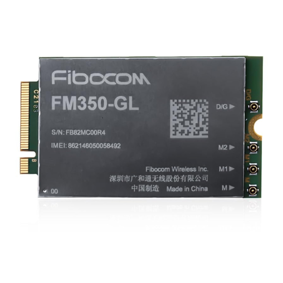
Structure Specification 6.1 Product Appearance The product appearance for FM350 module is shown in Figure 24: Figure 22. Module appearance 6.2 Dimensions of Structure The structural dimensions of the FM350 module is shown in Figure 25: Copyright © Fibocom Wireless Inc. -
Page 76: Interface Model
Figure 25. Based on the nomenclature shown in Figure 26 for the M.2 module definition, FM350 module adopts Type 3052-S3-B interface (30x52mm, the component maximum height on t top layer is 1.5mm, PCB thickness is 0.8mm, and KEY ID is B). Copyright © Fibocom Wireless Inc. -
Page 77: Connector
Figure 27. For stack-up top-mount single-sided module, the recommended part number is APCI0144-P001A, manufactured by LOTES Corporation, and the dimension is shown in Figure 28. The package of connector, please refer to the specification. Copyright © Fibocom Wireless Inc. - Page 78 6 Structure Specification Figure 25. M.2 Dimensions of structure for stack-up Mid-mount single-sided module Figure 26. M.2 dimensions of structure for stack-up top-mount single-sided module Copyright © Fibocom Wireless Inc.
-
Page 79: Card Assembly
Figure 27. Angle of insertion for APCI0144-P001A Figure 28. Angle of insertion for APCI0026-P001A 6.5.2 Mid-mount Connection with Single-Sided Module Stack-up Mid-mount (In-line) single-sided module is shown in Figure 31. The maximum height of components is 1.5mm. Copyright © Fibocom Wireless Inc. -
Page 80: Top-Mount Connection With Single-Sided Module
Stack-up top-mount single-sided module is shown in Figure 32. The maximum height of components is 1.5mm. Figure 30. Stack-up top-mount single-sided module 1) 2.75mm maximum above mother board 2) Full keep out area 30×52mm below module, which means don’t place any Copyright © Fibocom Wireless Inc. -
Page 81: Storage
The FM350 module uses tray package, 20 pcs are packed in each tray, with 5 trays including one empty tray on top in each box and 5 boxes in each case. Tray packaging process is shown Copyright © Fibocom Wireless Inc. - Page 82 6 Structure Specification in Figure 33: Copyright © Fibocom Wireless Inc.
-
Page 83: Tray Size
6 Structure Specification Figure 31. Tray packaging process 6.7.2 Tray Size The pallet size is 330 mm×175 mm×6.5 mm, and is shown in Figure 34: Figure 32. Tray size (unit: mm) Copyright © Fibocom Wireless Inc. -
Page 84: Appendix
Analog Input /Output Open Drain Tristate Internal pull up Internal pull down Hi-Z High impedance Not connected Output high level effective voltage Output low level effective voltage Input high level effective voltage Input low level effective voltage Copyright © Fibocom Wireless Inc. - Page 85 General Purpose Digital Output General Purpose Digital Input Specific Absorption Rate Inter-Process Communication UVLO Under voltage lock out RFFE RF frond end PLDR Platform-level Device Reset 8.NCC 警语 1. 減少電磁波影響,請妥適使用 2. 電波功率密度 MPE 標準值為:____ mW/cm²,送測產品實測值為:____ mW/cm²,建議使用 時設備天線至少距離人體____ 公分。 Copyright © Fibocom Wireless Inc.
- Page 86 CE Conformance information The device could be used with a separation distance of 20cm to the human body. Hereby, [Fibocom Wireless Inc.] declares that the radio equipment type [FM350-GL-16] is in compliance with Directive 2014/53/EU. The full DoC can be found at https://www.fibocom.com/en/downloadcenter/index.html.
- Page 87 Fibocom Wireless Inc. that they wish to change the antenna trace design. In this case, a Class II permissive change...
- Page 88 FCC ID/IC ID cannot be used on the final product. In these circumstances, the OEM integrator will be responsible for re-evaluating the end product (including the transmitter) and obtaining a separate FCC/IC authorization. Copyright © Fibocom Wireless Inc.
- Page 89 - Reorient or relocate the receiving antenna. - Increase the separation between the equipment and receiver. - Connect the equipment into an outlet on a circuit different from that to which the receiver is connected. Copyright © Fibocom Wireless Inc.
- Page 90 2 conditions above are met, further transmitter test will not be required. However, the OEM integrator is still responsible for testing their end-product for any additional compliance requirements required with this module installed. Copyright © Fibocom Wireless Inc.
- Page 91 Radiation Exposure Statement This equipment complies with IC radiation exposure limits set forth for an uncontrolled environment. This equipment should be installed and operated with minimum distance 20 cm between the radiator & your body. Copyright © Fibocom Wireless Inc.
- Page 92 2) Le module émetteur peut ne pas être coïmplanté avec un autre émetteur ou antenne. Tant que les 2 conditions ci-dessus sont remplies, des essais supplémentaires sur l'émetteur ne seront pas nécessaires. Toutefois, l'intégrateur OEM est toujours responsable des essais sur Copyright © Fibocom Wireless Inc.
- Page 93 This transmitter module is authorized only for use in device where the antenna may be installed such that 20 cm may be maintained between the antenna and users. The final end product must be labeled in a visible area with the following: “Contains IC:21374-FM350GL16”. Copyright © Fibocom Wireless Inc.
- Page 94 à la façon d'installer ou de supprimer ce module RF dans le manuel de l'utilisateur du produit final qui intègre ce module. Le manuel de l'utilisateur final doit inclure toutes les informations réglementaires requises et avertissements comme indiqué dans ce manuel. Copyright © Fibocom Wireless Inc.
Need help?
Do you have a question about the FM350-GL-16 and is the answer not in the manual?
Questions and answers