Table of Contents
Advertisement
Advertisement
Table of Contents

Subscribe to Our Youtube Channel
Related Manuals for Fibocom FM101-GL


Summary of Contents for Fibocom FM101-GL
- Page 1 FM101-GL Hardware Guide V1.3...
- Page 2 All the statements, information and suggestions contained in the document do not constitute any explicit or implicit guarantee. Trademark The trademark is registered and owned by Fibocom Wireless Inc. Contact Website: https://www.fibocom.com/en/ Address: Floor 10, Building A, Shenzhen International Innovation Valley, First Stone Road,...
-
Page 3: Table Of Contents
3.3 Control Signal ......................28 3.3.1 Module Start-Up ....................28 3.3.1.1 Start-up Circuit ....................28 3.3.1.2 Start-up Timing Sequence ................29 3.3.2 Module Shutdown ....................30 3.3.3 Module Reset ......................31 3.4 USIM Interface ......................34 Copyright © Fibocom Wireless Inc. - Page 4 4.3 Transmitting Power ....................50 4.4 Receiver Sensitivity ..................... 52 4.4.1 Dual Antennas Receiver Sensitivity ..............52 4.5 GNSS ..........................55 4.6 Antenna Design ......................56 5 ESD Characteristics ..................60 6 Structure Specification ................61 Copyright © Fibocom Wireless Inc.
- Page 5 6.5.2 Mid-mount Connection with Single-Sided Module ........65 6.5.1 Top-mount Connection with Single-Sided Module ........66 6.6 Storage .......................... 67 6.6.1 Storage Life ......................67 6.7 Packaging ........................67 6.7.1 Tray Package ......................68 6.7.2 Tray Size ........................69 Copyright © Fibocom Wireless Inc.
-
Page 6: Applicable Model
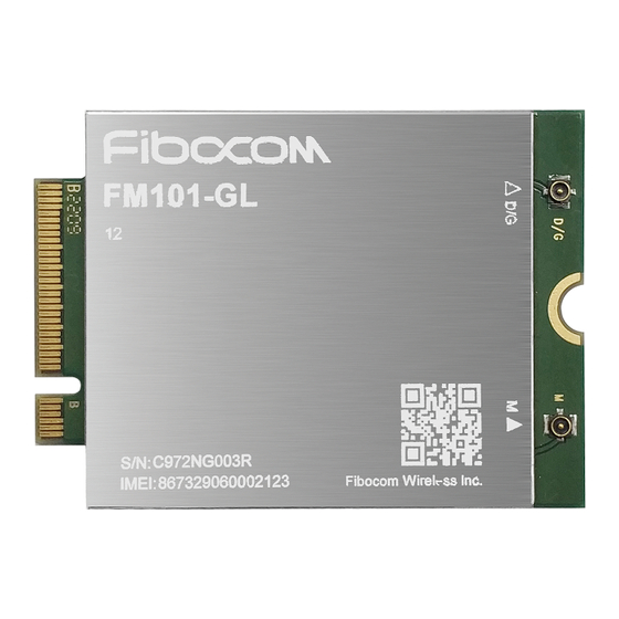
Applicable Model Applicable Model Applicable Model Description Qualcomm SDX12 platform. 4G communication module FM101-GL-12 with M.2 interface for Global. USB only for data transmission. Copyright © Fibocom Wireless Inc. -
Page 7: Change History
Update pin map Update B39 notice. B39 support in japan. V1.2 (2022-01-25) Update USB2.0 description. V1.1 (2022-01-19) Add notice about B48 don’t support in IC. Support USB2.0 data transmission. V1.0 (2021-09-22) Draft version. Copyright © Fibocom Wireless Inc. -
Page 8: Foreword
1.1 Introduction The document describes the electrical characteristics, RF performance, dimensions and application environment, etc. of FM101-GL (hereinafter referred to as FM101). With the assistance of the document and other instructions, the developers can quickly understand the hardware functions of FM101 modules and develop products. -
Page 9: Related Documents
3GPP TS 27.005 V10.0.1: Use of Data Terminal Equipment - Data Circuit terminating Equipment (DTE-DCE) interface for Short Message Service (SMS) and Cell Broadcast Service (CBS) PCI Express M.2 Specification Rev4.0 1.3 Related Documents Copyright © Fibocom Wireless Inc. -
Page 10: Overview
B1/2/4/5/6/8/19 GNSS GPS/GLONASS/Galileo/BDS Data Throughput LTE Peak DL 300Mbps (CAT12)/UL 50Mbps (CAT4) DL UMTS: 384 kbps/UL 384 kbps UMTS/HSPA+ Peak DL DC-HSPA+: 42 Mbps (CAT24)/UL 5.76 Mbps (CAT6) Modulation Characteristic LTE Modulation 3GPP Release 12 Copyright © Fibocom Wireless Inc. -
Page 11: Key Features
Qualcomm SDX12, 14nm process, ARM Cortex-A7, up to 1.28 GHz Memory 2Gb LPDDR2+2Gb NAND Flash Supported OS Windows 10/Chrome /Linux Power Supply DC 3.135V to 4.4V, typical 3.3V Normal operating temperature: –10°C to +55°C Temperature Extended operating temperature: –30°C to +75°C Copyright © Fibocom Wireless Inc. - Page 12 Dual SIM (one embedded eSIM), 1.8V/3V USB 2.0 USB 3.0 W_Disable# Function Interface Bodysar Tunable antenna I2C (Reserved) Software Protocol Stack IPV4/IPV6 AT Commands 3GPP TS 27.007 and 27.005 Firmware USB2.0 Update Multiple carrier Other Feature Windows MBIM support Copyright © Fibocom Wireless Inc.
-
Page 13: Application Block
2.4 Application Block The peripheral applications for FM101 module are shown in Figure 1: ANT1(D/G) ANT0(M) Module Power eSIM Supply USB2.0/ ON/OFF# RESET# SIM1 EINT Indicator USB3.0 Host application Control Card Figure 1. Application block Copyright © Fibocom Wireless Inc. -
Page 14: Hardware Block Diagram
RF functions. Baseband contains: UMTS/LTE TDD/LTE FDD controller PMU MCP (NAND+ LPDDR2) Application interface RF contains: RF Transceiver RF DCDC/PA RF Duplexer Antenna Connector Copyright © Fibocom Wireless Inc. -
Page 15: Antenna Configuration
B1/2/4/5/6/8/19 B1/2/4/5/6/8/19 Main antenna LTE Band LTE Band ANT0 (M) 617–3800 port for TRX B1/2/3/4/5/7/8/12/13/14/17/1 B1/2/3/4/5/7/8/12/13/14/17/18/ 8/19/20/25/26/28/30/66/71/3 19/20/25/26/28/29/30/66/71/38 8/39/40/41/42/43/48 /39/40/41/42/43/48 WCDMA B1/2/4/5/6/8/19 LTE Band Antenna port ANT1 (D/G) 617–3800 B1/2/3/4/5/7/8/12/13/14/17/18/ for RX 19/20/25/26/28/29/30/66/71/38 /39/40/41/42/43/48 GNSS Copyright © Fibocom Wireless Inc. -
Page 16: Application Interface
UIM1_CLK USB3.0-Tx+ UIM1_RESET USB3.0-Tx‐ GPIO(I) W_DISABLE2#(3.3/1.8V) DPR(3.3/1.8V) VIO_1.8V WOWWAN#(1.8V) GPIO(I) CONFIG_0 GPIO(I) Notch Notch Notch Notch Notch Notch Notch Notch LED1#(3.3V OD) USB D- W_DISABLE1#(3.3/1.8V) USB D+ FULL_CARD_POWER_OFF#(3.3/1.8V) +3.3V +3.3V CONFIG_3 Figure 3. Pin map Copyright © Fibocom Wireless Inc. -
Page 17: Pin Definition
Power Output Digital Input Digital Output Digital Input /Output Analog Input Analog Output Analog Input /Output Open Drain Tristate Internal pull up Internal pull down Hi-Z High impedance Not connected The pin definition is as follows: Copyright © Fibocom Wireless Inc. - Page 18 0.3-3V WWAN disable, default high, W_DISABLE1# 3.3/1.8V active low USB D- I/O - USB data minus 0.3-3V System status LED, output open LED1# OD T 3.3V drain, CMOS 3.3V Power Supply Notch Notch Notch Notch Copyright © Fibocom Wireless Inc.
- Page 19 1.8V output for ANT Tuner, PO PD Supply reserved. /1.8V Dynamic power reduction detect, 3.3/1.8V default high, active low GNSS disable, default high, active W_DISABLE2# 3.3/1.8V low, reserved Power Supply GPIO GPIO(I), default low, reserved 1.8V Copyright © Fibocom Wireless Inc.
- Page 20 Power Supply I2C clock, master mode,default I2C_SCL 1.8V high, reserved I2C data, master mode, default I2C_SDA I/O PU 1.8V high, reserved I2C interrupt, used for wake up I2C_IRQ# 1.8V I2C host, default high, reserved Power Copyright © Fibocom Wireless Inc.
- Page 21 RFFE clock Power Supply MIPI interface tunable ANT, RFFE_SDATA I/O PD 1.8V RFFE data ANTCTL0 Tunable ANT CTRL0, default low 1.8V Wireless coexistence between WWAN and WIFI/BT modules, COEX3 1.8V based on BT-SIG coexistence protocol. COEX_EXT_FTA, Copyright © Fibocom Wireless Inc.
- Page 22 (390KΩ), active high WWAN reset input, internal pull RESET# 1.8V up (22KΩ), active low GND, FM101 M.2 module is CONFIG_1 configured as the WWAN – SSIC, USB 3.0 interface type Power +3.3V Power input Supply Power Copyright © Fibocom Wireless Inc.
-
Page 23: Power Supply
Table 6. Power interface DC Parameter (V) Pin Name Pin Description Minimum Typical Maximu Value Value m Value 2, 4, 70, Power supply +3.3V 3.135 72, 74 input 1.8V power output ANT_TUNER_1V8 1.71 1.89 for antenna tuner Copyright © Fibocom Wireless Inc. -
Page 24: Power Supply
Power supply input 2500 1.8V power output for ANT_TUNER_1V8 antenna tuner UIM1_PWR USIM power supply 3.2.1 Power Supply The FM101 module should be powered through the +3.3V pins, and the power supply design is shown in Figure: Copyright © Fibocom Wireless Inc. - Page 25 Filter out the interference generated 1uF, 100nF Digital signal noise from the clock and digital signals 700/800, 850/900 MHz Filter out low frequency band RF 39pF, 33pF frequency band interference 18pF, 10pF, 1500/1800, 2100/2300, Filter out medium/high frequency band Copyright © Fibocom Wireless Inc.
-
Page 26: Logic Level
Figure 5. Power supply requirement 3.2.2 Logic Level The FM101 module 1.8V logic level definition is shown in the following table: Table 9. Module 1.8V logic level definition Parameter Minimum Typical Maximum Unit 1.71 1.89 1.89 @1mA -0.3 Copyright © Fibocom Wireless Inc. -
Page 27: Power Consumption
Typical Parameter Mode Condition Current (mA) Power off Power supply, module power off DRX=6 WCDMA DRX=8 DRX=9 Sleep Paging cycle #128 frames (1.28s DRx LTE FDD cycle) LTE TDD Paging cycle #128 frames (1.28s DRx Copyright © Fibocom Wireless Inc. - Page 28 LTE FDD Data call Band 8 @24dBm LTE FDD Data call Band 12 @24dBm LTE FDD Data call Band 13 @24dBm LTE FDD Data call Band 14 @24dBm LTE FDD Data call Band 17 @24dBm Copyright © Fibocom Wireless Inc.
- Page 29 LTE TDD Data call Band 48 @21dBm The above data is the average value obtained by testing the sample for high/medium/low channels in room temperature(ambient 25℃). LTE TDD test is under the uplink downlink configuration 1 condition. Copyright © Fibocom Wireless Inc.
-
Page 30: Control Signal
AP (Application Processor) controls the module start-up. The recommended design is using a default PD port to control FCPO#. It also should reserve a 100KΩ(NC) pull down resistor on AP side. The circuit design is shown in Figure: Copyright © Fibocom Wireless Inc. -
Page 31: Start-Up Timing Sequence
The start-up timing is shown in Figure: +3.3V FCPO# RESET# typical TBDs Module State Initialization Activation(AT Command Ready) Figure 7. Timing control for start-up Recommende Index Min. Max. Comment The delay time of power supply rising from 0V up Copyright © Fibocom Wireless Inc. -
Page 32: Module Shutdown
(the reverse process of initialization), and it will be completed after tsd time (tsd is the waiting time from AP send AT+CPWROFF to AP receive OK, the max tsd is 5s). The control timing is shown in Figure 8: Copyright © Fibocom Wireless Inc. -
Page 33: Module Reset
The FM101 module can reset to its initial status by pulling down the RESET# signal for more than 20ms, and module will restart after RESET# signal is released. When customer executes RESET# function, the PMU power will be turned off. The recommended circuit design is shown in the Figure 9: Copyright © Fibocom Wireless Inc. - Page 34 (including whole power off and power on sequence, t can refer section 3.3.2), recommend using in system warm boot. +3.3V FCPO# RESET# off1 typical TBD Module State Activation Baseband reset Initialization Activation Figure 10. Reset timing 1st Copyright © Fibocom Wireless Inc.
- Page 35 RF interference and protected by GND. Also, the RESET# signal lines shall neither near the PCB edge nor route on the surface planes to avoid module from reset caused by ESD problems. Copyright © Fibocom Wireless Inc.
-
Page 36: Usim Interface
SIM card is inserted; and 1.8V low level indicates SIM card is detached. 3.4.2 USIM Interface Circuit 3.4.2.1 N.C. SIM Card Slot The reference circuit design for N.C. (Normally Closed) SIM card slot is shown in Figure 12: Copyright © Fibocom Wireless Inc. -
Page 37: Sim Card Slot
SIM1_DETECT pin high. 3.4.2.2 N.O. SIM Card Slot The reference circuit design for N.O. (Normally Open) SIM card slot is shown in Figure 13: Figure 13. Reference circuit for N.O. SIM card slot Copyright © Fibocom Wireless Inc. -
Page 38: Usim Hot-Plug
SIM card is inserted when the SIM_DETECT pin is high, then executes the initialization program and finish the network registration after reading the SIM card information. When the SIM_DETECT pin is low, the module determines that the SIM card is detached and does not read the SIM card. Copyright © Fibocom Wireless Inc. -
Page 39: Usim Design
FM101 module, please refer to Universal Serial Bus Specification 2.0” and “Universal Serial Bus Specification 3.0”. FM101 FW update only can base on USB2.0 interface. So it should still confirm USB2.0's connected. If only use USB3.0 does date communication. Copyright © Fibocom Wireless Inc. -
Page 40: Usb Interface Definition
0.5pF TVS diodes. USB_D- and USB_D+ are high speed differential signal lines with the maximum transfer rate of 480 Mbit/s, so the following rules shall be followed carefully in the case of PCB layout: Copyright © Fibocom Wireless Inc. -
Page 41: Usb3.0 Interface Application
The two pairs differential signal lines should be parallel and have the equal length. The right angle routing should be avoided. The two pairs differential signal lines should be routed on the layer that is adjacent to the ground layer, and wrapped with GND vertically and horizontally. Copyright © Fibocom Wireless Inc. -
Page 42: Status Indicator
Module Status LED1# Signal RF function ON Low level (LED on) RF function OFF High level (LED off) The LED driving circuit is shown in figure 16: Figure 16. LED driving circuit Copyright © Fibocom Wireless Inc. -
Page 43: Interrupt Control
The module enters into flight mode after the RF function is disabled. The definition of W_DISABLE1# signal is as follows: W_DISABLE1# Function signal High/Floating WWAN function is enabled, the module exits the flight mode. WWAN function is disabled, the module enters into flight mode. Copyright © Fibocom Wireless Inc. -
Page 44: Dpr
1.8V output for antenna tuner. The pin definition is as below table: Pin Name I/O Reset Value Pin Description Level 1.8V power output for antenna ANT_TUNER_1V8 PO PD 1.8V tuner, reserved Tunable ANT control, MIPI Interface, RFFE_SCLK 1.8V RFFE clock Copyright © Fibocom Wireless Inc. -
Page 45: Configuration Interface
WWAN – SSIC, USB 3.0 interface type GND, FM101 M.2 module is CONFIG_1 configured as the WWAN – SSIC, USB 3.0 interface type GND, FM101 M.2 module is CONFIG_2 configured as the WWAN – SSIC, Copyright © Fibocom Wireless Inc. - Page 46 The M.2 module configuration is shown in the following table: Config_0 Config_1 Config_2 Config_3 Module Type and Main Port (pin21) (pin69) (pin75) (pin1) Host Interface Configuration WWAN–SSIC Please refer to “PCI Express M.2 Specification Rev4.0” for more details. Copyright © Fibocom Wireless Inc.
-
Page 47: Radio Frequency
“D/G” is for Diversity antenna, which is used to receive the diversity RF signal and GNSS signal. Figure 17. RF connectors 4.1.2 RF Connector Characteristic Rated Condition Environment Condition Frequency Range DC-6GHz Temperature Range: –40°C-+85°C Characteristic 50Ω Impedance Copyright © Fibocom Wireless Inc. -
Page 48: Rf Connector Dimensions
FM101 module uses standard M.2 RF connectors. The RF connector part number is 818004607 manufactured by ECT cooperation, and the size is 2×2×0.6mm. The connector dimension is shown as following picture: Figure 18. RF connector dimensions Figure 19. 0.81mm coaxial antenna dimensions Copyright © Fibocom Wireless Inc. -
Page 49: Rf Connector Assembly
To avoid damage in RF connector mating, it is recommended using pulling JIG as Figure 22, and the pulling JIG must be lifted up vertically to PCB surface (see Figure 23 and 24). Pulling JIG must be lifted up vertically to PCB surface (see Figure 23 and 24). Copyright © Fibocom Wireless Inc. -
Page 50: Operating Band
4.2 Operating Band The operating bands of FM101 module are shown in the following table: Operating Band Description Mode Tx (MHz) Rx (MHz) Band 1 2100MHz LTE FDD/WCDMA 1920-1980 2110-2170 Band 2 1900MHz LTE FDD/WCDMA 1850-1910 1930-1990 Copyright © Fibocom Wireless Inc. - Page 51 LTE FDD 716-728 Band 30 2300MHz LTE FDD 2305-2315 2350-2360 Band 66 1700MHz LTE FDD 1710-1780 2110-2200 Band 71 680MHz LTE FDD 663-698 617-652 Band 38 2600MHz LTE TDD 2570-2620 Band 39 1900MHZ LTE TDD 1880-1920 Copyright © Fibocom Wireless Inc.
-
Page 52: Transmitting Power
Band 2 24+1.7/-3.7 23.5±1 Band 4 24+1.7/-3.7 23.5±1 WCDMA Band 5 24+1.7/-3.7 23.5±1 Band 6 24+1.7/-3.7 23.5±1 Band 8 24+1.7/-3.7 23.5±1 Band 19 24+1.7/-3.7 23.5±1 LTE FDD Band 1 23±2.7 23±1 10MHz Bandwidth, 1 RB Copyright © Fibocom Wireless Inc. - Page 53 10MHz Bandwidth, 1 RB Band 66 23±2.7 23±1 10MHz Bandwidth, 1 RB Band 71 23+2.7/-3.2 24±1 10MHz Bandwidth, 1 RB Band 38 23±2.7 23±1 10MHz Bandwidth, 1 RB LTE TDD Band 39 23±2.7 23±1 10MHz Bandwidth, 1 RB Copyright © Fibocom Wireless Inc.
-
Page 54: Receiver Sensitivity
All bands support dual antennas, the receiver sensitivity for each band of FM101 module is shown in below table: 3GPP Requirement Rx Sensitivity Mode Band Note (dBm) Typical(dBm) WCDMA Band 1 -106.7 BER < 0.1% Copyright © Fibocom Wireless Inc. - Page 55 Band 3 -93.3 Bandwidth 10MHz Band 4 -96.3 Bandwidth LTE FDD 10MHz Band 5 -94.3 Bandwidth 10MHz Band 7 -94.3 Bandwidth 10MHz Band 8 -93.3 Bandwidth 10MHz Band 12 -93.3 Bandwidth Band 13 -93.3 10MHz Copyright © Fibocom Wireless Inc.
- Page 56 10MHz Band 25 -92.8 Bandwidth 10MHz Band 26 -93.8 Bandwidth 10MHz Band 28 -94.8 Bandwidth 10MHz Band 29 -93.3 Bandwidth 10MHz Band 30 -95.3 Bandwidth 10MHz Band 66 -95.8 Bandwidth 10MHz Band 71 -93.5 Bandwidth Copyright © Fibocom Wireless Inc.
-
Page 57: Gnss
The above values are measured in dual antennas condition (Main+Diversity). For single main antenna (without Diversity), the sensitivity will drop about 3dBm for each band of LTE. 4.5 GNSS FM101 module supports GPS/GLONASS/BDS/GALILEO and adopts RF Diversity and GNSS integrated antenna. Copyright © Fibocom Wireless Inc. -
Page 58: Antenna Design
GPS+ BDS+ GLONASS+ Galileo Acquisition GNSS current is tested with RF disabled at 25°C temperature. 4.6 Antenna Design The FM101 module provides two antenna interfaces, and the antenna design requirements are shown in the following table: Copyright © Fibocom Wireless Inc. - Page 59 LTE Band 14 (700): 40 MHz LTE Band 17 (700): 42 MHz LTE Band 18 (800): 80 MHz LTE Band 19 (800): 80 MHz LTE band 20 (800): 71 MHz LTE band 25 (1900):145 MHz Copyright © Fibocom Wireless Inc.
- Page 60 > 28 dBm average power WCDMA & LTE Recommended standing- ≤2:1 wave ratio (SWR) ANT on B30 suggestion: Peak gain < 1dBi, for FCC EIRP requirement, Efficient > 50% for carrier TRP requirement. If integrator doesn't follow the Copyright © Fibocom Wireless Inc.
- Page 61 4 Radio Frequency instruction, may cause FCC EIRP or carrier TRP certification fail. Copyright © Fibocom Wireless Inc.
-
Page 62: Esd Characteristics
The ESD characteristics are shown in the following table (Temperature: 25°C, Relative Humidity: 40%). Interface Contact Discharge Air Discharge ±8 kV ±15 kV Antenna Interface ±8 kV Golden Finger ±1KV ESD performance is based on EVB-M2 development board. Copyright © Fibocom Wireless Inc. -
Page 63: Structure Specification
The product appearance for FM101 module is shown in Figure 25: Figure 25. Module appearance The label of each module is subject to the good shipped. 6.2 Dimension of Structure The structural dimension of the FM101 module is shown in Figure 26: Copyright © Fibocom Wireless Inc. -
Page 64: Interface Model
Figure 27 Dimension of Structure. Based on the M.2 interface definition, FM101 module adopts Type 3042-S3-B interface (30 x 42 mm, the component maximum height on t top layer is 1.5 mm, PCB thickness is 0.8 mm, and KEY ID is B). Copyright © Fibocom Wireless Inc. -
Page 65: Connector
Figure 28. For stack-up top-mount single-sided module, the recommended part number is APCI0144-P001A, manufactured by LOTES Corporation, and the dimension is shown in Figure 29. The package of connector, please refer to the specification. Copyright © Fibocom Wireless Inc. - Page 66 6 Structure Specification Figure 28. M.2 Dimensions of structure for stack-up Mid-mount single-sided module Figure 29. M.2 dimensions of structure for stack-up top-mount single-sided module Copyright © Fibocom Wireless Inc.
-
Page 67: Card Assembly
Figure 30. Angle of insertion for APCI0144-P001A Figure 31. Angle of insertion for APCI0026-P001A 6.5.2 Mid-mount Connection with Single-Sided Module Stack-up Mid-mount (In-line) single-sided module is shown in Figure 32. The maximum height of components is 1.5 mm. Copyright © Fibocom Wireless Inc. -
Page 68: Top-Mount Connection With Single-Sided Module
Stack-up top-mount single-sided module is shown in Figure 33. The maximum height of components is 1.5 mm. Figure 33. Stack-up top-mount single-sided module 2.75 mm maximum above mother board. Full keep out area 30 mm × 42 mm Copyright © Fibocom Wireless Inc. -
Page 69: Storage
The module is a precision electronic product, and may suffer permanent damage if no correct electrostatic protection measures are taken. Copyright © Fibocom Wireless Inc. -
Page 70: Tray Package
The FM101 module uses tray package, 20 pcs are packed in each tray, with 5 trays including one empty tray on top in each box and 5 boxes in each case. Tray packaging process is shown in Figure 34: Figure 34. Tray packaging process Copyright © Fibocom Wireless Inc. -
Page 71: Tray Size
6.7.2 Tray Size The pallet size is 315 mm × 170 mm × 6.5 mm, and is shown in Figure 35: Figure 35. Tray size (unit: mm) ITEM DIM (Unit: mm) 315.0±2.0 170.0±2.0 6.5±0.3 0.8±0.1 43.0±0.3 31.0±0.3 Copyright © Fibocom Wireless Inc. - Page 72 6 Structure Specification 79.0±0.2 60.0±0.2 180.0±0.2 60.0±0.2 40.0±0.2 Copyright © Fibocom Wireless Inc.
- Page 73 Fibocom that they wish to change the antenna trace design. In this case, a Class II permissive change application is required to be filed by...
- Page 74 Federal Communication Commission Interference Statement This device complies with Part 15 of the FCC Rules. Operation is subject to the following two conditions: (1) This device may not cause harmful interference, and (2) this device must accept any interference received, including interference that may cause undesired operation. This equipment has been tested and found to comply with the limits for a Class B digital device, pursuant to Part 15 of the FCC Rules.
- Page 75 This device is intended only for OEM integrators under the following conditions: (For module device use) 1) The antenna must be installed such that 20 cm is maintained between the antenna and users, and 2) The transmitter module may not be co-located with any other transmitter or antenna. As long as 2 conditions above are met, further transmitter test will not be required.
- Page 76 Industry Canada Statement This device complies with Industry Canada’s licence-exempt RSSs. Operation is subject to the following two conditions: (1) This device may not cause interference; and (2) This device must accept any interference, including interference that may cause undesired operation of the device.
- Page 77 Cet appareil est conçu uniquement pour les intégrateurs OEM dans les conditions suivantes: (Pour utilisation de dispositif module) 1) L'antenne doit être installée de telle sorte qu'une distance de 20 cm est respectée entre l'antenne et les utilisateurs, et 2) Le module émetteur peut ne pas être coïmplanté avec un autre émetteur ou antenne. Tant que les 2 conditions ci-dessus sont remplies, des essais supplémentaires sur l'émetteur ne seront pas nécessaires.
- Page 78 Manual Information to the End User The OEM integrator has to be aware not to provide information to the end user regarding how to install or remove this RF module in the user’s manual of the end product which integrates this module. The end user manual shall include all required regulatory information/warning as show in this manual.
Need help?
Do you have a question about the FM101-GL and is the answer not in the manual?
Questions and answers