Table of Contents
Advertisement
Quick Links
Advertisement
Table of Contents

Subscribe to Our Youtube Channel
Related Manuals for Fibocom L-831-EA


Summary of Contents for Fibocom L-831-EA
- Page 1 L831-EA Module Hardware User Manual Version: V1.0.1 Date: 2015-02-12...
- Page 2 Copyright ©2015 Fibocom Wireless Inc. All rights reserved. Trademarks Notice The FIBOCOM Logo is registered by Fibocom Wireless Inc. All other product or service names or logos are the property of their respective owners. Copyright ©2015 Fibocom Wireless Inc. All rights reserved.
- Page 3 FOR FCC Federal Communications Commission (FCC) Declaration of Conformity This device complies with part 15 of the FCC Rules. Operation is subject to the following two conditions: (1) This device may not cause harmful interference, and (2) this device must accept any interference received, including interference that may cause undesired operation.
-
Page 4: Important Note
IMPORTANT NOTE: This module is intended for OEM integrator. The OEM integrator is still responsible for the FCC compliance requirement of the end product, which integrates this module. 20cm minimum distance has to be able to be maintained between the antenna and the users for the host this module is integrated into. Under such configuration, the FCC radiation exposure limits set forth for an population/uncontrolled environment can be satisfied. - Page 5 Revision History Version Date Remarks V1.0.0 2014-12-30 Initial version V1.0.1 2015-02-12 Update the consumption and the power on/off timing L831-EA Module Hardware User Manual Page 5 of 43...
- Page 6 Applicability Table Type Note L831-EA The difference of L831-EA wireless module as listed below: Model Type LTE FDD WCDMA GSM/GPRS/EDGE Band L831-EA 1,2,3,4,5,7,8,13,17, Band 1,2,4,5,8 850/900/1800/1900MHz 18,19,20 L831-EA Module Hardware User Manual Page 6 of 43...
-
Page 7: Table Of Contents
Contents IMPORTANT NOTE:..............................4 1 Preface..................................10 1.1 Outline................................10 1.2 Standards..............................10 2 Introduction................................12 2.1 Description..............................12 2.2 Specifications...............................12 2.3 Appearance..............................15 3 Mechanical................................16 3.1 Dimension..............................16 3.2 Application Interface Description......................17 3.3 M.2 Connector............................. 18 4 Hardware Overview..............................19 4.1 Pins Definition..............................19 4.1.1 Pins Number.............................19 4.1.2 Pins Description.......................... - Page 8 5.5.1 USIM Pins............................30 5.5.2 Description of USIM........................30 5.5.2.1 “Normally Closed”SIM Circuit Design................30 5.5.2.2 “Normally Open” SIM Circuit Design.................31 5.5.3 USIM Design Points........................31 5.5.4 USIM Hot Plug..........................32 5.5.4.1 Hardware Connection......................32 5.5.4.2 Software Configuration......................32 5.6 Digital Audio..............................32 5.6.1 Description of I2S Interface......................33 5.6.2 Description of PCM Interface......................33 5.7 Android/Win8Dual System Switch Control Interface................34...
- Page 9 7.2.2 Impedance Design...........................42 7.3 Antenna Design............................42 7.3.1 Antenna Design Requirements..................... 42 L831-EA Module Hardware User Manual Page 9 of 43...
-
Page 10: Preface
1 Preface 1.1 Outline The document outlines the electrical, RF performance, mechanical size and application environment of L831-EA wireless module. Under the help of the document and others application notice, the application developer could understand quickly the performance of L831-EA series wireless module, and developing the product. - Page 11 3GPP TS 23.090 -v6.1.0: Unstructured Supplementary Service Data (USSD); Stage 2 3GPP TS 24.008 v6.19, Mobile radio interface Layer 3 specification; 3GPP TS 25.101 V7.18.0: User Equipment (UE) radio transmission and reception (FDD) 3GPP TS 36.101 V9.18.0: User Equipment (UE) radio transmission and reception ...
-
Page 12: Introduction
2 Introduction 2.1 Description L831-EA modules are highly integrated LTE M.2 wireless communication modules, supports 3 module 12 band and the global main 4G/3G/2G modes (LTE FDD/WCDMA/GSM) These bands support the mobile operators `cellular network of the Europe & Asia-Pacific and American marketing. 2.2 Specifications Specifications L831-EA... - Page 13 Digital Audio Audio Voice coders :EFR/HR/FR/AMR VoLTE (not support yet) Audio Control Gain control Character Set IRA,GSM,UCS2,HEX FIBOCOM proprietary AT commands AT commands GSM 07.05 GSM 07.07 Firmware Loader Tool over USB Accessories User Manual Developer Kit L831-EA Module Hardware User Manual...
- Page 14 Note: 1. Please make sure the temperature for device will not be higher than 55˚C. 2. The minimum distance between the user and/or any bystander and the radiating structure of the transmitter is 20cm. 3. Assessment of compliance of the product with the requirements relating to the Radio and Telecommunication Terminal Equipment Directive (EC Directive 1999/5/EC) was performed by PHOENIX TESTLAB (Notified Body No.0700), L831-EA Module Hardware User Manual...
-
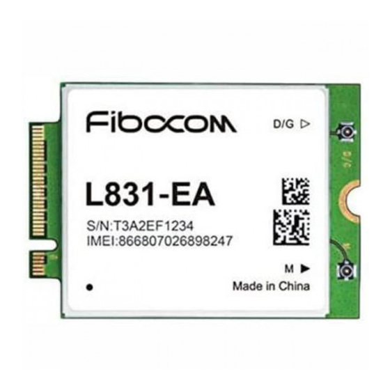
Page 15: Appearance
2.3 Appearance The following pictures show the L831-EA wireless module. Top view: Figure 2- 1 Top View Bottom view: Figure 2- 2 Bottom View L831-EA Module Hardware User Manual Page 15 of 43... -
Page 16: Mechanical
3 Mechanical 3.1 Dimension Figure3- 1Dimension Diagram L831-EA Module Hardware User Manual Page 16 of 43... -
Page 17: Application Interface Description
3.2 Application Interface Description L831-EA module uses 75-pin gold fingers as the external interface, the size of the module please refer to the section3.1. As shown in Figure 4-2, L831-EA module uses the 75-pin fingers interface (67pin is the signal interface and Pin8 is notch). -
Page 18: Connector
3.3 M.2 Connector Recommend to use the M.2 connector from LOTES, the type is APCI0026-P001A,the package of connector design please refer to the relevant specifications. As shown in Figure 3-2: Figure 3-2 Size of APCI0026-P001A M.2 connector L831-EA Module Hardware User Manual Page 18 of 43... -
Page 19: Hardware Overview
4 Hardware Overview 4.1 Pins Definition 4.1.1 Pins Number CONFIG_2 +3.3V +3.3V +3.3V CONFIG_1 CLK32K RESET# SIM_DETECT ANTCTL3 ANTCTL2 ANTCTL1 ANTCTL0 TX_BLANKING SYSCLK GNSS_IRQ GNSS_SDA GNSS_SCL SSIC-TXP/USB3.0-TX+(NC) UIM_PWR SSIC-TXN/USB3.0-TX-(NC) UIM_DATA UIM_CLK SSIC-RXP/USB3.0-RX+(NC) UIM_RESET SSIC-RXN/USB3.0-RX-(NC) I2S_WA W_DISABLE2# I2S_RX WOWWAN# I2S_TX CONFIG_0 I2S_CLK Notch Notch... -
Page 20: Pins Description
CONFIG_3 Figure4- 2 Pins Definition (Top View) 4.1.2 Pins Description The description of L831-EA pins as listed below: Reset Idle Pin# Name Description Value Value The internal connects with GND, the CONFIG_3 interface type of L831-EA module is WWAN-SSIC0. The main power input, the voltage +3.3V range is: 3.135V ~ 4.4V The main power input, the voltage... - Page 21 module is WWAN-SSIC0 I2S_RX I2Sserial data output, CMOS 1.8V The module wake up the Host device WOWWAN# signal,low level is available,CMOS 1.8V. I2S_TX I2Sserial data input, CMOS 1.8V Body SAR Detect,CMOS 1.8V GPS Disable signal, low level is W_DISABLE2# available, CMOS 1.8V (not support yet).
- Page 22 The switch interrupt signal of GNSS_IRQ Win8/Android system. SYSCLK 26MHz clock output. GSM TDMA Timer output signal, the TX_BLANKING GPS control signal, CMOS 1.8V Tunable antenna control signal ANTCTL0 GPO,CMOS 1.8V (not support yet) Tunable antenna control signal, MIPI ANTCTL1 RFFE SDATA, CMOS 1.8V (not support yet) Tunable antenna control signal, MIPI...
- Page 23 will be pulled up. External reset signal input, CMOS RESET# 1.8V CLK32K 32KHz clock output. The internal connects with GND, the CONFIG_1 interface type of L831-EA module is WWAN-SSIC0. The main power input, the voltage +3.3V range is : 3.135V ~ 4.4V The main power input, the voltage +3.3V range is : 3.135V ~ 4.4V...
-
Page 24: Hardware Interface
5 Hardware Interface 5.1 Power Interface 5.1.1 Power Supply L831-EA module requires a 3.135V~ 4.4V DC power supply to provide the maximum GSM emission current with 2A. Input power supply requirements as listed below: Parameters Minimum Recommended Maximum Unit +3.3V 3.135 Note: 1. -
Page 25: Power On/Off And Reset Signal
5.2 Power on/off and Reset Signal L831-EA wireless module supports 2 control signals for the modules` power on/off and the reset operation. The definition of the pins as listed below: Pin# Pin Name Electrical Level Description FUL_CARD_POWER_OFF# CMOS 1.8V Power on/off signal RESET# CMOS 1.8V External reset signal input. -
Page 26: Recommended Circuit Design Of Power On/Off Signals
off it, pull down the FUL_CARD_POWER_OFF# or floating. For details as listed below: Off modes Methods Condition Software Send AT+CPWROFF commands. Normal power_off Only used for system halted or happens Pull down the FUL_CARD_POWER_OFF# Hardware exceptions and the software modes can or floating. -
Page 27: Reset Signal
Figure 5- 3 the recommended design of FUL_CARD_POWER_OFF# signal 5.2.2 RESET Signal L831-EA wireless module supports external reset function. The module can back to initial state through Reset _N signal. While the RESET# signal is active low and keep 100ms, the module will reset and restart. The internal PMU cannot power cut while the clients execute the RESET function. -
Page 28: Index Signal
5.3 Index Signal 5.3.1 Index Signal Pins L831-EA module used for providing drain output signal and indicate RF condition: Pin # Name Description Close or open the condition indication of RF network, CMOS 3.3V LED1# The condition description of LED1# signal as listed below : Condition LED1# RF open... -
Page 29: Application For Usb Interface
Modem COM port is so slow, and cannot up to 100Mbpss, the uplink requirements of LTE. So it is not suggested. The Modem COM can be used to initiate data services temporarily only while the client`s NCM port is useless. 5.4.2 Application for USB Interface The recommended circuit design as follows: Figure5- 6 Recommended circuit design of USB interface... -
Page 30: Usim Pins
5.5.1 USIM Pins Pin# Name Type Description UIM_PWR USIM power supply signal UIM_RESET USIM Reset signal UIM_CLK USIM clock signal UIM_DATA USIM data signal The detection signal for SIM insetting The default is 390K ohm resistance pulled up and SIM_DETECT input. -
Page 31: Normally Open" Sim Circuit Design
5.5.2.2 “Normally Open” SIM Circuit Design Referenced Circuit Design: Figure5- 8 “Reference Design of “Normally open” SIM Card Interface Normally Open SIM Connector: 1)Pull out SIM card, pin 7 and pin 8 disconnect. 2)Inset SIM card, pin 7 and pin 8 short-circuit . Note: ... -
Page 32: Usim Hot Plug
The signal lines of SIM cards shall do some ESD protection , and it request to choose the ESD protected components with low capacitance, such as Zener diode. Recommend the clients to use the ESD components and the equivalent capacitance shall be less than 33pF. ESD components shall near to SIM card interfaces while layout. -
Page 33: Description Of I2S Interface
The description of I2S signal as listed below: Pin# Name Type Description I2S2_CLK Bit clock I2S2_WA0 Left- right clock (LRCK) I2S2_TX Serial data output I2S2_RX Serial data input 5.6.1 Description of I2S Interface L831-EA Signal Direction Audio CODEC I2S Port I2S_CLK I2S_CLK I2S_WA... -
Page 34: Android/Win8Dual System Switch Control Interface
configuration of data transmission. Supports various audio sample rates (48KHz,44.1KHz,32KHz, 24KHz,22.5KHz,16KHz,12KHz,8KHz, 11.025KHz). Note: Cause the timing of I2S modes is easier than PCM modes and easier to fit, recommend clients to use transmission audio of I2S mode. While transmission with PCM modes, the PCM timing sequence is difficult to fit to make the tone quality become bad. -
Page 35: Description Of Gps_Disable# Interface
W_DISABLE# Function WWAN closed High WWAN opened The function of WWAN defined by AT commands , and keep open by Floating default . 5.8.2 Description of GPS_DISABLE# Interface L831-EA module provides through hardware to open/close GPS function signal, this function can also control by AT commands. -
Page 36: Body_Sar Interface
5.11 BODY_SAR Interface L831-EA module supports BODY_SAR (DPR pin) function. BODY_SAR is input signal (the signal is output directly by the AP end), with high level by default, and low level is effectively. While the human nearing, AP can detect it through the distance sensor, then output the BODY_SAR signal with low level. -
Page 37: Rf Interface
CONFIG_3 Connect to GND within the module CONFIG_0 CONFIG_1 Connect to GND within the module CONFIG_2 Connect to GND within the module The configuration of M.2 Socket 2 Module as listed below : Config_0 Config_1 Config_2 Config_3 Module Type and Main Port Configuration (pin21) (pin69) -
Page 38: Main Performance Of Rf Connector
Figure 5-10 Structure diagram of RF connecting seat Figure 5-11 0.81mm coaxial line Figure 5-12 RF connector insert into RF connecting seat 5.15.3Main Performance of RF Connector Rated conditions Environment condition L831-EA Module Hardware User Manual Page 38 of 43... -
Page 39: Other Interfaces
Frequency range DC to 6GHz Temperature range : Characteristic impedance 50Ω –40°C to +85°C 5.16 Other Interfaces The following interfaces are not supported now: GPIO and Tunable ANT. L831-EA Module Hardware User Manual Page 39 of 43... -
Page 40: Electrical And Environmental
6 Electrical and Environmental 6.1 Electrical This table shows the electrical features range of L831-EA module. Parameter Minimum Value Maximum Value Unit Power supply Digital Signal 6.2 Environmental This table shows the environmental features of L831-EA module Parameter Minimum Value Maximum Value Unit Operational Temperature... -
Page 41: Rf Interface
7 RF Interface 7.1 Operating Band 7.1.1 Antenna Band Operating Description Mode Tx (MHz) Rx (MHz) Band Band 1 IMT 2100MHz LTE FDD/WCDMA 1920 - 1980 2110 - 2170 Band 2 PCS 1900MHz LTE FDD/WCDMA/GSM 1850 - 1910 1930 - 1990 Band 3 DCS 1800MHz LTE FDD/GSM... - Page 42 7.2.2 Impedance Design The impedance of RF signal lines should be controlled within 50ohm. 7.3 Antenna Design 7.3.1 Antenna Design Requirements (1) Antenna Efficiency Antenna efficiency is the ratio of antenna input power to radiation power. Cause the return loss, material loss, and coupling loss, the radiation power is always lower than the input power.
- Page 43 or do some filtering on the routing. (7)TRP/TIS TRP (Total Radiated Power): GSM850/900>28dBm GSM DCS1800/PCS1900 >25dBm WCDMA Band 1,2,4,5,8>19dBm LTE FDD Band 1,2,3,5,7,8,13,17,18,19,20 >19dBm TIS (Total Isotropic Sensitivity): GSM850,GSM 900,DCS1800,PCS1900 <-102dBm WCDMA Band1,2,4,5,8<-102dBm LTE FDD Band1,2,3,5,7,8,13,17,18,19,20 <-95dBm (10MHz band width) L831-EA Module Hardware User Manual Page 43 of 43...
Need help?
Do you have a question about the L-831-EA and is the answer not in the manual?
Questions and answers