Table of Contents
Advertisement
Quick Links
Advertisement
Table of Contents

Related Manuals for Fibocom NL668-LA


Summary of Contents for Fibocom NL668-LA
- Page 1 FIBOCOM NL668-LA Hardware User Manual Version: V1.0.0 Date: 2019-06-06 69100.1000.00.02.61.34_DEMO" Reproduction forbidden without Fibocom Wireless Inc. written authorization - All Rights Reserved. FIBOCOM NL668-LA Series Hardware User Manual Page 1 of 65...
- Page 2 Applicability type Product model Description MCP is 4+2,support MAIN_ANT, DIV_ANT, GNSS_ANT NL668-LA Reproduction forbidden without Fibocom Wireless Inc. written authorization - All Rights Reserved. FIBOCOM NL668-LA Series Hardware User Manual Page 2 of 65...
- Page 3 The trademark is registered and owned by Fibocom Wireless Inc. Versions Record Version Author Assessor Approver Update Date Description V1.0.0 Gaoying Tumin Chenguojiang 2019-06-06 Initial version Reproduction forbidden without Fibocom Wireless Inc. written authorization - All Rights Reserved. FIBOCOM NL668-LA Series Hardware User Manual Page 3 of 65...
-
Page 4: Table Of Contents
5.3.2 (U)SIM interface circuit ......................... 34 5.3.3 (U)SIM hot plug ..........................35 5.3.4 (U)SIM design requirements ....................... 36 5.4 USB interface ............................ 37 Reproduction forbidden without Fibocom Wireless Inc. written authorization - All Rights Reserved. FIBOCOM NL668-LA Series Hardware User Manual Page 4 of 65... - Page 5 8.1.1 Absolute voltage range ......................... 54 8.1.2 Operating voltage range ......................54 8.2 Environment temperature range ....................54 Reproduction forbidden without Fibocom Wireless Inc. written authorization - All Rights Reserved. FIBOCOM NL668-LA Series Hardware User Manual Page 5 of 65...
- Page 6 11.2 Terms and acronyms ........................62 11.3 Related Document .......................... 64 11.4 Reference Standards ........................64 11.5 Contact ............................. 65 Reproduction forbidden without Fibocom Wireless Inc. written authorization - All Rights Reserved. FIBOCOM NL668-LA Series Hardware User Manual Page 6 of 65...
- Page 7 Figure 7- 2 GNSS Antenna Reference Circuit..................52 Figure 9- 1 Product Appearance ........................ 57 Figure 9- 2 Structure Dimension (Unit: mm) ..................... 57 Reproduction forbidden without Fibocom Wireless Inc. written authorization - All Rights Reserved. FIBOCOM NL668-LA Series Hardware User Manual Page 7 of 65...
- Page 8 Table 7- 5 GNSS Specification ........................49 Table 7- 6 Main Antenna Requirements ....................51 Table 8- 1 Absolute Voltage Range ......................54 Reproduction forbidden without Fibocom Wireless Inc. written authorization - All Rights Reserved. FIBOCOM NL668-LA Series Hardware User Manual Page 8 of 65...
- Page 9 Table 11- 3 EGPRS Modulation and Encoding Method ................ 61 Table 11- 4 Terms and Acronyms ....................... 64 Reproduction forbidden without Fibocom Wireless Inc. written authorization - All Rights Reserved. FIBOCOM NL668-LA Series Hardware User Manual Page 9 of 65...
-
Page 10: Introduction
Product manufacturers need to communicate the following safety instructions to end users. In case of failure to comply with these safety rules, Fibocom Wireless will not be responsible for the consequences caused by the user’s misuse. - Page 11 There is a safety hazard in operating electronic equipment in any potentially explosive environment. Reproduction forbidden without Fibocom Wireless Inc. written authorization - All Rights Reserved. FIBOCOM NL668-LA Series Hardware User Manual Page 11 of 65...
-
Page 12: Product Overview
2 Product Overview 2.1 Product Introduction The NL668-LA series wireless module is a broadband wireless terminal product applicable to various network formats and multi-bands include TDD-LTE /FDD-LTE /WCDMA /GSM. 2.2 Product Specification Specification LTE FDD: Band 1,2,3,4,5,7,8,12,17,28,66 LTE TDD: Band 38,40... -
Page 13: Functional
When the temperature is beyond the normal operating temperature range (-30 ° C to + 75 ° C), the RF performance of the module may slightly exceed the 3GPP specification. 2.3 Functional Functional of the NL668-LA series module, including baseband and RF features. Baseband includes: ... -
Page 14: Evaluation Board
2.4 Evaluation Board Fibocom provide EVK-GT8230-NL, ADP-NL668-LA evaluation board to convenient module's debug and use. Reproduction forbidden without Fibocom Wireless Inc. written authorization - All Rights Reserved. FIBOCOM NL668-LA Series Hardware User Manual Page 14 of 65... -
Page 15: Pin Description
3 Pin Description 3.1 Pin Assignment The NL668-LA series module is available in 144 pins. The numbers of the LCC pins are 80, and the LGA pins are 64. the top view of the pin assignment is shown as follow figure: Figure 3- 1 Pin Assignment (Top View Diagram) Note: “85 ~112”... - Page 16 Power output Analog input Analog output Open drain Open collector Table 3- 1 I/O Description Parameters The pin function description of NL668-LA series module is shown as table 3-2: Pin Num Pin Name Level Description min=-0.3V External device wake-up module, low max=0.6V...
- Page 17 For 3.0V (U)SIM: max=0.45V min=2.55V For 1.8V (U)SIM: max=0.45V USIM_RST min=1.35V (U)SIM reset signal For 3.0V (U)SIM: max=0.45V Reproduction forbidden without Fibocom Wireless Inc. written authorization - All Rights Reserved. FIBOCOM NL668-LA Series Hardware User Manual Page 17 of 65...
- Page 18 PCM clock signal max=0.6V min=1.2V max=2.0V SDC2_DATA3 Reserved SDC2_DATA2 Reserved SDC2_DATA1 Reserved SDC2_DATA0 Reserved SDC2_CLK Reserved SDC2_CMD Reserved VREG_L13_2P85 Reserved Reproduction forbidden without Fibocom Wireless Inc. written authorization - All Rights Reserved. FIBOCOM NL668-LA Series Hardware User Manual Page 18 of 65...
- Page 19 VBAT_BB Vmin=3.3V Vnorm=3.8V Vmax=4.3V VBAT_BB Vmin=3.3V Baseband Power Input (3.3V~4.3V) Vnorm=3.8V min=1.35V STATUS Module network state indicate max=0.45V Reproduction forbidden without Fibocom Wireless Inc. written authorization - All Rights Reserved. FIBOCOM NL668-LA Series Hardware User Manual Page 19 of 65...
- Page 20 USB differential data bus (-) specification Vmax=5.25V USB_VBUS Vmin=3.0V USB plug detection Vnorm=5.0V 72,76 Ground 73,82 RESERVED Reserved 74,75,77 ~81,83,8 85~112 Reproduction forbidden without Fibocom Wireless Inc. written authorization - All Rights Reserved. FIBOCOM NL668-LA Series Hardware User Manual Page 20 of 65...
- Page 21 Reserved BT_EN Reserved Reserved RESERVED Reserved RESERVED Reserved RESERVED Reserved RESERVED Table 3- 2 Pin function description Note: Reproduction forbidden without Fibocom Wireless Inc. written authorization - All Rights Reserved. FIBOCOM NL668-LA Series Hardware User Manual Page 21 of 65...
- Page 22 Keep the unused pins floating. The reserved pins are in development Reproduction forbidden without Fibocom Wireless Inc. written authorization - All Rights Reserved. FIBOCOM NL668-LA Series Hardware User Manual Page 22 of 65...
-
Page 23: Electrical Characteristics
In the rest of the document, VBAT includes VBAT_BB and VBAT_RF. 4.2 Power supply The NL668-LA series module needs to be powered by the VBAT pin. The recommend power design is shown in Figure 4-1: Figure 4- 1 Recommend Power Design Table 4-1 is the filter capacitors design of power supply: Reproduction forbidden without Fibocom Wireless Inc. -
Page 24: Output
4.3 1.8V output The NL668-LA series module outputs a 1.8V voltage through the VDD_EXT for the use of the internal digital circuit of module. The voltage is the logic level of the module and can be used to indicate module Power on/off, or for external low current (<80mA) circuits. -
Page 25: Power Consumption
Table 4- 3 VDD_EXT Logic Level 4.4 Power consumption The power consumption of NL668-LA series module measured at 3.8V power supply is shown as follow table, for USB sleep and USB wakeup AT commands please refer to 6.1.2 section: Parameter... - Page 26 LTE FDD LTE-RMS @+23dBm LTE FDD Data transfer Band 4 @+23dBm LTE FDD Data transfer Band 5 @+23dBm Reproduction forbidden without Fibocom Wireless Inc. written authorization - All Rights Reserved. FIBOCOM NL668-LA Series Hardware User Manual Page 26 of 65...
- Page 27 LTE FDD Data transfer Band 66 @+23dBm Data transfer Band @+23dBm LTE TDD Data transfer Band @+23dBm Table 4- 4 Power Consumption Reproduction forbidden without Fibocom Wireless Inc. written authorization - All Rights Reserved. FIBOCOM NL668-LA Series Hardware User Manual Page 27 of 65...
-
Page 28: Functional Interface
5.1.1 Power on/off 5.1.1.1 Power on When NL668-LA series module in power off mode, pull down PWRKEY pin 100ms~2s, the module will power on, it is recommended to use OC/OD drive circuit to control PWRKEY pin. The OC drive reference... - Page 29 VBAT enable and pull down PWRKEY pin at least 30ms. 5.1.1.2 Power off The module supports three power off methods as table 5-2. Reproduction forbidden without Fibocom Wireless Inc. written authorization - All Rights Reserved. FIBOCOM NL668-LA Series Hardware User Manual Page 29 of 65...
-
Page 30: Reset
Pull down RESET_N pin 700s~1s, then release it Sent AT commands AT+RESET Software reset Table 5- 3 Reset Reproduction forbidden without Fibocom Wireless Inc. written authorization - All Rights Reserved. FIBOCOM NL668-LA Series Hardware User Manual Page 30 of 65... - Page 31 Figure 5- 5 OC Driven Reset Reference Circuits Figure 5- 6 Button Reset Reference Circuits The reset timing is shown as follows: Reproduction forbidden without Fibocom Wireless Inc. written authorization - All Rights Reserved. FIBOCOM NL668-LA Series Hardware User Manual Page 31 of 65...
-
Page 32: Network Status Indicate Interface
Figure 5- 7 Reset Timing 5.2 Network status indicate interface NL668-LA series module provides three network status indicate pins. Pin 5 is network status indicator by default, AT commands AT+LEDCFG can switch to pin6 or pin61, table 5-4 is the pin definition. -
Page 33: U)Sim Card Interface
Figure 5- 8 Network Indicate Light Reference Circuits 5.3 (U)SIM card interface NL668-LA series module has built-in (U)SIM card interface, and supports 1.8V and 3.0V (U)SIM card. 5.3.1 (U)SIM pin definition (U)SIM pin definition is shown in the following table:... -
Page 34: U)Sim Interface Circuit
POL are disconnected when there is no card. The following is the reference design circuit, (U)SIM card insert, USIM_PRESENCE pin is high level; (U)SIM card pull out, USIM_PRESENCE pin is low level. Reproduction forbidden without Fibocom Wireless Inc. written authorization - All Rights Reserved. FIBOCOM NL668-LA Series Hardware User Manual... -
Page 35: U)Sim Hot Plug
Figure 5- 11 (U)SIM Card Connector without Detection Signal Reference Circuit 5.3.3 (U)SIM hot plug NL668-LA series module support (U)SIM hot plug function, it determines the insertion and removal of (U)SIM card by detect the USIM_ PRESENCE pin state. The card hot plug function can be configured by the “AT+MSMPD” command, and the AT commands are shown in the following table: Reproduction forbidden without Fibocom Wireless Inc. -
Page 36: U)Sim Design Requirements
USIM_CLK and USIM_DATA signals are ground isolated to avoid mutual interference. If it is difficult to do so, (U)SIM signal needs to be ground protected as a set; Reproduction forbidden without Fibocom Wireless Inc. written authorization - All Rights Reserved. FIBOCOM NL668-LA Series Hardware User Manual... -
Page 37: Usb Interface
5.5 UART Interface 5.5.1 UART interface definition NL668-LA series module has two serial ports: the main serial port and debug serial port. The main serial ports support 4800bps, 9600bps, 19200bps, 38400bps, 57600bps, 115200bps, 230400bps baud rate. The default baud rate is 115200bps, used for data transmission and AT command transmission. -
Page 38: Uart Port Application
Module Transmit data Table 5- 11 Debug Serial Port 5.5.2 UART port application The serial port level of NL668-LA series module is 1.8V, if the level of the client host system is 3.3V or other, level translator needed between the module and the host. The reference design circuit of level... -
Page 39: Adc Interface
ADC1 Analog to digital converter interface 1 Table 5- 12 ADC Pin Definitation 5.7 PCM interface NL668-LA series module provides a PCM interface for communication with digital audio devices such as an external CODEC. 5.7.1 Support model Product model Description... -
Page 40: Pcm Interface Definition
(Falling edge sampling) Table 5- 15 PCM Interface Description NL668-LA series module adopts the above configuration by default, any adjustment please contact Fibocom Wireless technical support. 5.7.4 PCM signal description The PCM signal of NL668-LA series module adopts domestic mainstream Europe E1 standard. - Page 41 PCM_DOUT valid Delay from PCM_CLK falling – – t(zdout) PCM_DOUT high impedance Table 5- 16 Codec Timing Parameters Reproduction forbidden without Fibocom Wireless Inc. written authorization - All Rights Reserved. FIBOCOM NL668-LA Series Hardware User Manual Page 41 of 65...
-
Page 42: Low Power Consumption
Draw out the USB cable or disable the USB HUB controller, module enter sleep mode. Wake up: Plug in USB cable or enable the USB HUB controller can wake up the module. Reproduction forbidden without Fibocom Wireless Inc. written authorization - All Rights Reserved. FIBOCOM NL668-LA Series Hardware User Manual Page 42 of 65... -
Page 43: Usb Application (Nonsupport Usb Suspend, Nonsupport Vbus)
(X=0, WAKEUP_IN pin is high level, module enter sleep mode; X=1, WAKEUP_IN pin is low level, module enter sleep mode) Reproduction forbidden without Fibocom Wireless Inc. written authorization - All Rights Reserved. FIBOCOM NL668-LA Series Hardware User Manual Page 43 of 65... -
Page 44: Uart Application ( Dtr Pin Level Control )
If you want to use the RI signal to represent the state of the module, please refer to the Reproduction forbidden without Fibocom Wireless Inc. written authorization - All Rights Reserved. FIBOCOM NL668-LA Series Hardware User Manual Page 44 of 65... - Page 45 AT+GTWAKE command in FIBOCOM AT Commands User Manual_Sleep. For more sleep command description, please refer to 《FIBOCOM AT Commands User Manual_Sleep》 Reproduction forbidden without Fibocom Wireless Inc. written authorization - All Rights Reserved. FIBOCOM NL668-LA Series Hardware User Manual Page 45 of 65...
-
Page 46: Rf Interface
7 RF interface NL668-LA series module has ANT_MAIN, ANT_DIV and ANT_ GNSS three antenna interfaces, its pin definition show as table 7-1: Pin Name Pin Num. Description ANT_DIV Diversity antenna ANT_GNSS GPS antenna ANT_MAIN Main antenna Table 7- 1 RF Interface 7.1 Operating band... -
Page 47: Receive Sensitivity
Table 7- 3 Output Power 7.3 Receive Sensitivity Rx Sensitivity(dBm) RxD Sensitivity(dBm) Mode Band Typ. Typ. GSM 850 -109 Reproduction forbidden without Fibocom Wireless Inc. written authorization - All Rights Reserved. FIBOCOM NL668-LA Series Hardware User Manual Page 47 of 65... - Page 48 Band 66 -97.5 -98.5 Band 38 -97.5 -96.5 LTE TDD Band 40 -97.5 -96.5 Table 7- 4 Receive Sensitivity Reproduction forbidden without Fibocom Wireless Inc. written authorization - All Rights Reserved. FIBOCOM NL668-LA Series Hardware User Manual Page 48 of 65...
-
Page 49: Gnss Receiver
7.4 GNSS Receiver 7.4.1 GNSS specification NL668-LA series module support GNSS function and adopts Qualcomm Gen8 technology, its specification show as follows: Description Condition Typ. 70mA GNSS fixing Power 70mA GNSS tracking (AT+CFUN=0) 34mA Standby Cold start<58s TTFF GNSS Warm start<70s 7.5s... - Page 50 LTE band 2(1900): 140 MHz Bandwidth (LTE) LTE Band 3(1800): 170 MHz LTE Band 4(2100): 440 MHz LTE Band 5(850): 70 MHz Reproduction forbidden without Fibocom Wireless Inc. written authorization - All Rights Reserved. FIBOCOM NL668-LA Series Hardware User Manual Page 50 of 65...
-
Page 51: Antenna Reference Design
In addition, the RF cable connect with antenna, and the location of the fixed antenna also may affect its performance. NL668-LA series module’s three antenna all led by welding plate. recommended clients use the U.FL-R-SMT-1 antenna connector and corresponding match adapter cable. - Page 52 Keep the PCB LAYOUT straight, and reduce holes on the route to another layer; also avoid right-angle and acute-angle wiring. Reproduction forbidden without Fibocom Wireless Inc. written authorization - All Rights Reserved. FIBOCOM NL668-LA Series Hardware User Manual Page 52 of 65...
- Page 53 Ground around antenna must be keep connect with main ground. ⚫ For more design information please refer to《FIBOCOM RF Antenna Application Design Instruction》 Reproduction forbidden without Fibocom Wireless Inc. written authorization - All Rights Reserved. FIBOCOM NL668-LA Series Hardware User Manual Page 53 of 65...
-
Page 54: Reliability
8.1 Limiting voltage range The limiting voltage range is maximum voltage range that power supply and digital or analog input/output interfaces can withstand. 8.1.1 Absolute voltage range The absolute voltage range of NL668-LA series module is shown as table 8-1. Parameter description Unit... -
Page 55: Environmental Reliability Requirements
Table 8- 4 Environmental Reliability Requirements 8.4 ESD characteristics NL668-LA series module design has considered ESD issue and provided ESD protect measurements, but take ESD issue taken by module carrier and secondary development into consideration, developers should care ESD protection of module application terminal. In addition to considering anti-static treatment of packaging, please refer to recommended circuit of interface design in the document. - Page 56 Interface Air discharge Contact discharge Other port ± 1KV ± 0.5KV Table 8- 5 ESD Allowable Discharge Range Reproduction forbidden without Fibocom Wireless Inc. written authorization - All Rights Reserved. FIBOCOM NL668-LA Series Hardware User Manual Page 56 of 65...
-
Page 57: Structure Specification
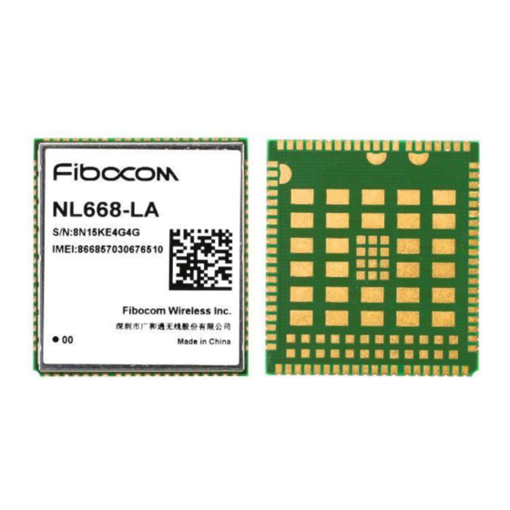
9 Structure specification 9.1 Product appearance The product appearance of NL668-LA series module is shown in Figure 9-1: Figure 9- 1 Product Appearance 9.2 Structure dimension The structure dimension of NL668-LA series module is shown as Figure 9-2: Figure 9- 2 Structure Dimension (Unit: mm) Reproduction forbidden without Fibocom Wireless Inc. -
Page 58: Pcb Soldering Pad And Stencil Design
9.3 PCB Soldering Pad and Stencil Design PCB soldering pad and stencil design please refer to《FIBOCOM NL668 LCC SMT Design Description》. 9.4 SMT SMT production process parameters and related requirements please refer to《FIBOCOM NL668 LCC SMT Design Description》. 9.5 Carrier and storage Carrier and storage please refer to《FIBOCOM NL668 LCC SMT Design Description》. -
Page 59: Approval
NL668-LA series module approval show as table 10-1: Certification Scheme NL668-LA Table 10- 1 Approval For more information please refer to Fibocom net. Reproduction forbidden without Fibocom Wireless Inc. written authorization - All Rights Reserved. FIBOCOM NL668-LA Series Hardware User Manual Page 59 of 65... -
Page 60: Appendix
Active timeslots indicate the total number of timeslots that the GPRS device can use for both uplink and downlink communications. Multislot Class Downlink Slots Uplink Slots Active Slots Reproduction forbidden without Fibocom Wireless Inc. written authorization - All Rights Reserved. FIBOCOM NL668-LA Series Hardware User Manual Page 60 of 65... - Page 61 MCS-8 8-PSK 54.4kbps 108.8kbps 217.6kbps MCS-9 8-PSK 59.2kbps 118.4kbps 236.8kbps Table 11- 3 EGPRS Modulation and Encoding Method Reproduction forbidden without Fibocom Wireless Inc. written authorization - All Rights Reserved. FIBOCOM NL668-LA Series Hardware User Manual Page 61 of 65...
-
Page 62: Terms And Acronyms
Downlink Carrier Aggregation SCell Secondary Cell for CA Mobile Equipment Mobile Station Mobile Terminated Printed Circuit Board Protocol Data Unit Reproduction forbidden without Fibocom Wireless Inc. written authorization - All Rights Reserved. FIBOCOM NL668-LA Series Hardware User Manual Page 62 of 65... - Page 63 Vmin Minimum Voltage Value VIHmax Maximum Input High Level Voltage Value VIHmin Minimum Input High Level Voltage Value Reproduction forbidden without Fibocom Wireless Inc. written authorization - All Rights Reserved. FIBOCOM NL668-LA Series Hardware User Manual Page 63 of 65...
-
Page 64: Related Document
⚫ 3GPP TS 36.521-1 V10.6.0: User Equipment (UE) conformance specification; Radio transmission and reception; Part 1: Conformance testing Reproduction forbidden without Fibocom Wireless Inc. written authorization - All Rights Reserved. FIBOCOM NL668-LA Series Hardware User Manual Page 64 of 65... -
Page 65: Contact
End user must follow the specific operating instructions for satisfying RF exposure compliance. This transmitter must not be co-located or operating in conjunction with any other antenna or transmitter. Reproduction forbidden without Fibocom Wireless Inc. written authorization - All Rights Reserved. FIBOCOM NL668-LA Series Hardware User Manual... - Page 66 Reproduction forbidden without Fibocom Wireless Inc. written authorization - All Rights Reserved. FIBOCOM NL668-LA Series Hardware User Manual Page 66 of 65...
Need help?
Do you have a question about the NL668-LA and is the answer not in the manual?
Questions and answers