National Instruments PXIe-4480 User Manual
Dynamic signal acquisition
Hide thumbs
Also See for PXIe-4480:
- Getting started manual (14 pages) ,
- Calibration procedure (34 pages)

Related Manuals for National Instruments PXIe-4480


Summary of Contents for National Instruments PXIe-4480
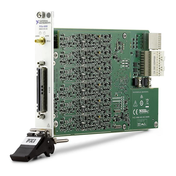
- Page 1 Dynamic Signal Acquisition PXIe-4480/4481 User Manual 6-Channel, 24-bit, 1.25 MS/s DSA Analog Input PXIe-4480/4481 User Manual October 2016 376368A-01...
- Page 2 11500 North Mopac Expressway Austin, Texas 78759-3504 USA Tel: 512 683 0100 For further support information, refer to the appendix. To comment on NI NI Services documentation, refer to the NI website at and enter the Info Code ni.com/info feedback © 2016 National Instruments. All rights reserved.
- Page 3 National Instruments Corporation. National Instruments respects the intellectual property of others, and we ask our users to do the same. NI software is protected by copyright and other intellectual property laws. Where NI software may be used to reproduce software or other materials belonging to others, you may use NI software only to reproduce materials that you may reproduce in accordance with the terms of any applicable license or other legal restriction.
- Page 4 ™ The ExpressCard word mark and logos are owned by PCMCIA and any use of such marks by National Instruments is under license. The mark LabWindows is used under a license from Microsoft Corporation. Windows is a registered trademark of Microsoft Corporation in the United States and other countries.
-
Page 5: Table Of Contents
Passband ......................3-3 Stopband ......................3-3 Alias-Free Bandwidth..................3-3 Filter Group Delay.................... 3-3 Time Domain Mode Acquisitions ................3-4 Analog Front End ..................... 3-4 Delta-Sigma ADC Modulator................3-4 Low Pass FIR Filter..................3-5 1/n Decimation ....................3-7 © National Instruments | v... - Page 6 Contents Time Domain Mode Considerations................. 3-8 Comparison to Frequency Domain Mode............3-8 Data Throughput ....................3-9 Timing and Triggering...................... 3-10 Sample Clock Timebase ...................3-10 External Clock ......................3-10 Timing Engines......................3-11 Digital Triggering ..................... 3-11 Analog Triggering..................... 3-11 Triggering and Filter Delay ..................3-12 Synchronization ........................
-
Page 7: Getting Started
PXIe-4480/4481 Dynamic Signal Acquisition (DSA) analog input module. Driver support for the PXIe-4480/4481 was first available in NI-DAQmx 16.1. For a list of devices supported by a specific release, refer to the NI-DAQmx Readme, available on the version-specific download page or installation media. -
Page 8: Specifications
Getting Started Specifications Refer to the PXIe-4480/4481 Specifications at for module specifications. ni.com/manuals Accessories Accessories for the PXIe-4480 and PXIe-4481 include the following shielded InfiniBand 12x cables: • SHB12X-6BNC (6 BNC analog inputs) • SHB12X-6MXLRM (6 mini-XLR analog inputs) •... -
Page 9: Using The Module
Input Connector Pinouts The PXIe-4480/4481 front panel has one 73-pin 12x InfiniBand connector. Figure 2-1 and Figure 2-2 show the pinout diagrams for the PXIe-4480 and the PXIe-4481, respectively. -
Page 10: Signal Descriptions
Chapter 2 Using the Module Figure 2-2. PXIe-4481 Pinout – – – – – – – – – – – – – – – – – – – – – – – – – – – – – – – – –... -
Page 11: Connecting Signals
Positive analog input signal (0 to 5) Negative analog input signal (0 to 5) — — Positive excitation (0 to 5), PXIe-4480 only EX GND Excitation ground (0 to 5), PXIe-4480 only — Ground — Shell Ground © National Instruments | 2-3... - Page 12 Chapter 2 Using the Module Table 2-3. BNC Connector Pin Assignments BNC Connector Pin Diagram Signal Name Signal Description Positive analog input signal (0 to 5) Negative analog input signal (0 to 5) Table 2-4. mXLR Connector Pin Assignments mXLR (Male) Connector Pin Diagram Signal Name...
-
Page 13: Front Panel Led Status
PXIe-4480/4481 User Manual Front Panel LED Status The PXIe-4480/4481 module uses two LEDs to indicate status and activity. Table 2-5 summarizes the functionality of the LEDs on the module. Table 2-5. PXIe-4480/4481 LED Descriptions State Description Access Module is not yet functional, or the module has detected a problem with a power rail. -
Page 14: Block Diagrams
Chapter 2 Using the Module Block Diagrams Figure 2-3 shows the PXIe-4480 analog input circuitry block diagram. Depending on the connector type, connect the signals as described in the section. Connecting Signals Figure 2-3. PXIe-4480 Analog Input Block Diagram EX<0..5>+ Excitation Voltage 10 V / 25 V / Adj (9.5 V to 12 V) - Page 15 Connecting Signals Figure 2-4. PXIe-4481 Analog Input Block Diagram AC/DC Coupling Programmable AI<0-5>+ Differential Lowpass Amplifier Filter 1.62 MΩ INPUT – – 1.62 MΩ AI<0-5>– Pseudodifferential Enable AC/DC Coupling 50 Ω © National Instruments | 2-7...
-
Page 16: Channel Types
The term pseudodifferential refers to the 50 Ω resistance between the negative input terminal and chassis ground. Attach the PXIe-4480/4481 to the chassis with the screws on the top and Note bottom of the front panel to provide a reliable ground connection. -
Page 17: Input Connections
In the charge measurement function (PXIe-4480 only), the negative input terminal is grounded. Input Connections Figure 2-5 shows the PXIe-4480/4481 voltage input connection with the terminals in differential configuration. Figure 2-5. PXIe-4480/4481 Voltage Input Connection in Differential Configuration... -
Page 18: Input Coupling
Input Coupling You can configure the PXIe-4480/4481 modules for either AC or DC coupling. If you select DC coupling, any DC offset present in the source signal is passed to the ADC. The DC-coupled configuration is usually best if the signal source has only small amounts of offset voltage or if the DC content of the acquired signal is important. -
Page 19: Iepe Excitation
Typical IEPE sensors have an enclosure that is electrically isolated from the Note IEPE electronics. As a result, connecting the sensor to the PXIe-4480 results in a floating connection even though the enclosure of the sensor is grounded. Transducer Electronic Data Sheet The PXIe-4480 supports Class 1 Transducer Electronic Data Sheet (TEDS) according to the IEEE 1451.4 standard. - Page 20 Chapter 2 Using the Module Figure 2-8 illustrates the internal construction of a powered/amplified sensor. Table 2-8 provides a guide for connecting signals from the PXIe-4480 to the sensor. Figure 2-8. Powered/Amplified Sensor +INPUT REGULATOR –INPUT +OUTPUT AMPLIFIER –OUTPUT Table 2-8. Powered/Amplified Sensor Connection...
-
Page 21: Fault Conditions
PXIe-4480/4481 User Manual Care must be exercised in this type of application, however, as the PXIe-4480 does not provide some of the features of a true strain measurement module, specifically remote sense of the excitation voltage. Without remote sense, the voltage present at the bridge will be slightly less than output by the module, due to the presence of lead wire resistance. -
Page 22: Overtemperature Detection
The PXIe-4480/4481 treats overtemperature as a non-fatal error in that the module can still be operated while in this condition. However, the integrity of the data being acquired may be compromised while the PXIe-4480/4481 is displaying an overtemperature condition. -
Page 23: Signal Acquisition
The PXIe-4480/4481 also supports time domain mode, in which the oversampled data is loosely filtered so that a maximum amount of bandwidth can be measured. Data may or may not be decimated. -
Page 24: Frequency Domain Mode Acquisitions
These frequencies are referred to as the ADC alias holes. To minimize the error from the ADC alias holes, the PXIe-4480/4481 modules feature a fixed-frequency analog filter. This analog filter removes high-frequency components in the analog signal path before they reach the ADC. -
Page 25: Passband
PXIe-4480/4481 and when the data associated with that event is available at the output of the acquisition and filtering process. This delay is called the group delay. In order to simplify the... -
Page 26: Time Domain Mode Acquisitions
Delta-Sigma ADCs. In time domain mode, these sharp filters are bypassed and the raw modulator data is sent directly to the FPGA of the PXIe-4480/4481 module where it is filtered. Figure 3-2 shows the FFT power spectrum of the modulator data when the analog inputs are shorted to ground with ±10 V range selected. -
Page 27: Low Pass Fir Filter
(ENOB) of 4.2 bits, which makes the acquisition nearly worthless. The PXIe-4480/4481 can be programmed with a symmetric FIR filter with up to 36 coefficients. Users can design their own filter and, using the NI-DAQmx Channel Property Node, program it to the PXIe-4480/4481. - Page 28 Refer to the PXIe-4480/4481 Specifications for more information about the default filter and the performance of time domain mode when using the default filter.
-
Page 29: 1/N Decimation
5 MS/s (n = 4), the hardware drops the first three samples coming from the digital filter and then returns the fourth sample. After sending a sample, the count starts over and the next three samples are dropped before sending the fourth. This pattern © National Instruments | 3-7... -
Page 30: Time Domain Mode Considerations
The returned samples do not pass through any additional filtering in the decimation process. The PXIe-4480/4481 supports decimation with n = 1 to 15. The lowest supported rate is 1.333333 MS/s (20 MS/s ÷15). Note that NI-DAQmx always coerces the requested sample rate up to the next sample rate that the hardware is capable of producing. -
Page 31: Data Throughput
Time (µs) Data Throughput The amount of data generated by a single PXIe-4480/4481 with all six channels acquiring at 20 MS/s can cause buffer overflow errors if the system is unable to transfer sample data from the device quickly enough. If this occurs, NI-DAQmx software will stop the acquisition and return error -200361, “Onboard device memory overflow…”... -
Page 32: Timing And Triggering
The PXIe-4480/4481 uses a x4 PXI Express connection to the PXI Express chassis backplane. Note that while the PXIe-4480/4481 will operate with a x1 connection, the amount of data that can be sent to the host computer will be limited and therefore tasks using multiple channels at higher sample rates may experience buffer overflow errors. -
Page 33: Timing Engines
Reference-triggered acquisitions can therefore only be configured as finite tasks. The analog trigger on the PXIe-4480/4481 cannot be used as a start trigger. This restriction is a result of the way the module compensates for the filter group delay. -
Page 34: Triggering And Filter Delay
Synchronization is important to minimize skew between channels and to eliminate clock drift between modules in long-duration operations. You can synchronize the analog input operations on two or more PXIe-4480/4481 modules to extend the channel count for your measurements. In addition, the PXIe-4480/4481 can synchronize with certain DSA modules, such as the PXIe-449x modules, using Reference Clock Synchronization. - Page 35 PXI Express chassis. Choose an arbitrary PXIe-4480/4481 master module to issue a sync pulse on one of the PXIe Trigger lines. The sync pulse resets the ADCs and oversample clocks, phase aligning all the clocks in the system to within nanoseconds.
-
Page 36: Ni Services
• System Integration—If you have time constraints, limited in-house technical resources, or other project challenges, National Instruments Alliance Partner members can help. To learn more, call your local NI office or visit ni.com/alliance © National Instruments | A-1... - Page 37 Appendix A NI Services • Training and Certification—The NI training and certification program is the most effective way to increase application development proficiency and productivity. Visit for more information. ni.com/training – The Skills Guide assists you in identifying the proficiency requirements of your current application and gives you options for obtaining those skills consistent with your time and budget constraints and personal learning preferences.
Need help?
Do you have a question about the PXIe-4480 and is the answer not in the manual?
Questions and answers