Table of Contents
Advertisement
Quick Links
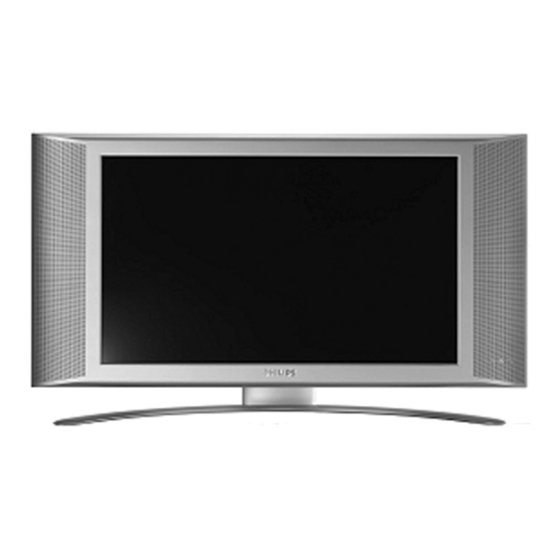
Colour Television
Contents
1
2
3
4
5
6
7
Electrical Diagrams and PWB lay-outs
TV Board: U_Cont
©
Copyright 2003 Philips Consumer Electronics B.V. Eindhoven, The Netherlands.
All rights reserved. No part of this publication may be reproduced, stored in a
retrieval system or transmitted, in any form or by any means, electronic,
mechanical, photocopying, or otherwise without the prior permission of Philips.
Published by RB 0370 Service PaCE
Page
2
5
6
39
44
51
53
54
55
56
57
58
59
60
61
Diagram PWB
(Diagram A1)
62
73-92
63
73-92
64
73-92
65
73-92
(Diagram A6)
66
73-92
(Diagram A7)
67
73-92
(Diagram A8)
68
73-92
73-92
73-92
(Diagram A10) 71
73-92
(Diagram A11) 72
73-92
93
94
(Diagram C1)
95
105-114
(Diagram C2)
96
105-114
Printed in the Netherlands
Contents
8
9
Subject to modification
Chassis
LC03U
AA
Page
(Diagram C3)
97
105-114
98
105-114
(Diagram C5)
99
105-114
100
105-114
101
105-114
(Diagram C8)
102
105-114
103
105-114
(Diagram C10) 104
105-114
115
116
115
117
(Diagram IN)
118
119
(Diagram IN1) 120
122
(Diagram IN2) 121
122
123
123
125
129
141
143
146
154
EN 3122 785 13611
Advertisement
Table of Contents

Related Manuals for Philips LC03U AA


Summary of Contents for Philips LC03U AA
-
Page 1: Table Of Contents
All rights reserved. No part of this publication may be reproduced, stored in a retrieval system or transmitted, in any form or by any means, electronic, mechanical, photocopying, or otherwise without the prior permission of Philips. Published by RB 0370 Service PaCE... -
Page 2: Technical Specifications, Connections, And Chassis Overview
EN 2 LC03U Technical Specifications, Connections, and Chassis Overview 1. Technical Specifications, Connections, and Chassis Overview Technical Specifications Connections 1.1.1 Reception 1.2.1 Front + Top Controls Tuning system : PLL TOP CONTROLS Color systems : 480p, 720p, 1080i MENU : NTSC 3.58, NTSC 4.43 : NTSC M (3.58 - 4.5) VOLUME... - Page 3 Technical Specifications, Connections, and Chassis Overview LC03U EN 3 1.2.3 Rear Connections Part 2 13 - H-sync 14 - V-sync 15 - Data clock Audio - PC/HD In 1 - Audio - R 0.5 V_rms/10 kohm S-Video 2 - Audio - L 0.5 V_rms/10 kohm Video In HD Video Input...
- Page 4 EN 4 LC03U Technical Specifications, Connections, and Chassis Overview Chassis Overview 1.3.1 15”/17” model TOP CONTROL PANEL LCD PANEL TO LCD PANEL Right Left Speaker Speaker INVERTER PANEL SIDE I/O PANEL TV BOARD FRONT LED PANEL ComPair SCALER BOARD CL 36532023_067.eps 140403 Figure 1-6 Chassis Overview 15”/17”...
-
Page 5: Safety Instructions, Warnings, And Notes
Safety Instructions, Warnings, and Notes LC03U EN 5 2. Safety Instructions, Warnings, and Notes Safety Instructions • Capacitor values may also use the value multiplier as the decimal point indication (e.g. 2p2 indicates 2.2 pF). • An 'asterisk' (*) indicates component usage varies. Refer to Safety regulations require that during a repair: the diversity tables for the correct values. -
Page 6: Directions For Use
EN 6 LC03U Directions for Use 3. Directions for Use... - Page 7 Directions for Use LC03U EN 7...
- Page 8 EN 8 LC03U Directions for Use...
- Page 9 Directions for Use LC03U EN 9...
- Page 10 EN 10 LC03U Directions for Use...
- Page 11 Directions for Use LC03U EN 11...
- Page 12 EN 12 LC03U Directions for Use...
- Page 13 Directions for Use LC03U EN 13...
- Page 14 EN 14 LC03U Directions for Use...
- Page 15 Directions for Use LC03U EN 15...
- Page 16 EN 16 LC03U Directions for Use...
- Page 17 Directions for Use LC03U EN 17...
- Page 18 EN 18 LC03U Directions for Use...
- Page 19 Directions for Use LC03U EN 19...
- Page 20 EN 20 LC03U Directions for Use...
- Page 21 Directions for Use LC03U EN 21...
- Page 22 EN 22 LC03U Directions for Use...
- Page 23 Directions for Use LC03U EN 23...
- Page 24 EN 24 LC03U Directions for Use...
- Page 25 Directions for Use LC03U EN 25...
- Page 26 EN 26 LC03U Directions for Use...
- Page 27 Directions for Use LC03U EN 27...
- Page 28 EN 28 LC03U Directions for Use...
- Page 29 Directions for Use LC03U EN 29...
- Page 30 EN 30 LC03U Directions for Use...
- Page 31 Directions for Use LC03U EN 31...
- Page 32 EN 32 LC03U Directions for Use...
- Page 33 Directions for Use LC03U EN 33...
- Page 34 EN 34 LC03U Directions for Use...
- Page 35 Directions for Use LC03U EN 35...
- Page 36 EN 36 LC03U Directions for Use...
- Page 37 Directions for Use LC03U EN 37...
- Page 38 EN 38 LC03U Directions for Use...
-
Page 39: Mechanical Instructions
Mechanical Instructions LC03U EN 39 4. Mechanical Instructions Index of this chapter: 1. Service Position 2. Stand Removal 3. Rear Cover Removal 4. Shield Removal 5. I/O Assy Removal 6. LED/Remote Control Board Removal 7. TV Board Removal 8. Scaler Board Removal 9. - Page 40 EN 40 LC03U Mechanical Instructions Figure 4-7 Bottom side connector plate • Use a 5 mm socket screwdriver to remove both connector distance bolts from the “PC input / VGA-in” socket. • Remove all shield mounting screws. Figure 4-4 TV rear cover removal 15”/17” model Continue with the paragraph 4.3.3.
- Page 41 Mechanical Instructions LC03U EN 41 I/O Removal To completely remove the Front LED panel incl. Lens), remove the assy screw. 4.5.1 Side I/O assy removal for 15/17 inch model TV Board Removal 4.7.1 For 15 /17inch model Disconnect all five TV board connectors out of the regarding sockets [3225], [1234], [1231], [1902], and [1732].
- Page 42 EN 42 LC03U Mechanical Instructions Scaler Board Removal 1. Carefully disconnect the cable connector in the centre of the Scaler board [1506]. Take care not to damage the fragile cables. 2. Disconnect the cable connectors at the edge of the Scaler board [1402] and [1003].
- Page 43 Mechanical Instructions LC03U EN 43 4.11 LCD Panel Removal 2. Unscrew the four screws, securing the panel frame to the LCD panel (see figures: “LCD panel mounting screws”). 3. Take off the panel frame while leading the panel connector 4.11.1 For 15 /17 inch model through the access hole in the frame Note: the LCD Panel is available in two versions: a TN-display and an IPS-display.
-
Page 44: Service Modes, Error Messages, And Repair Tips
EN 44 LC03U Service Modes, Error Messages, and Repair Tips 5. Service Modes, Error Messages, and Repair Tips Index of this chapter: 1. Test Points SDM Menu 2. Service Modes S D M 3. Errors T Y P E : 1 7 P F 9 9 4 5 / 3 7 H R S : 0 0 2 9 4. - Page 45 Service Modes, Error Messages, and Repair Tips LC03U EN 45 5.2.3 Service Alignment Mode (SAM) • To return to the main menu / previous menu, press “MENU” keys on the remote control Purpose of SAM: • To do alignments. Access to Normal User Menu •...
- Page 46 EN 46 LC03U Service Modes, Error Messages, and Repair Tips 1. Select “INSTALL” menu. 2. Select “CHANNEL EDIT”. T Y P E : 1 7 P F 9 9 4 5 / 3 7 H R S : 0 0 2 9 C S M 1 3.
- Page 47 Service Modes, Error Messages, and Repair Tips LC03U EN 47 5.3.2 Error codes When none of these devices responds to the micro controller for a prolonged time, the micro controller assumes that there is a failure in the 5V supply. By starting In case of non-intermittent faults, clear the error buffer before up the set with the service jumpers shorted, the 5V starting the repair, to prevent that “old”...
- Page 48 (COM) port of your PC and the PC connector (marked with 'PC') of the ComPair interface. ComPair (Computer Aided Repair) is a service tool for Philips 3. Connect the mains adapter to the supply connector Consumer Electronics products. ComPair is a further (marked with 'POWER 9V DC') of the ComPair interface.
- Page 49 Service Modes, Error Messages, and Repair Tips LC03U EN 49 7. Plug the mains adapter in a mains outlet, and switch the • Measure across C2913/C2933 (diagram A10). +8V3/+5V4 interface 'ON'. The green and red LEDs light up together. should be present respectively. If not present, probably this The red LED extinguishes after approx.
- Page 50 EN 50 LC03U Service Modes, Error Messages, and Repair Tips Menu text not sharp enough • Press “Smart Picture” button on the remote control. In case the picture improves, decrease the contrast value. The new “Personal Preference” value is automatically stored after 3 minutes.
-
Page 51: Block Diagrams
Block Diagrams, Testpoint Overviews, and Wiring Diagram LC03U 6. Block Diagrams, Testpoint Overviews, and Wiring Diagram Block Diagram (Tuner-IF-Video) TO 3D COMBFILTER PNL (23" ONLY) +5V4 VIDEO & QSS IF VDP - COLOUR PROCESSING VDP - COLOUR PROCESSING TUNER +8V3A SCL-0 C-SYNC GENERATOR MAIN-CBVS-EXT-IN... -
Page 52: Block Diagram (Tv Control And Inverter Panel)
Block Diagrams, Testpoint Overviews, and Wiring Diagram LC03U Block Diagram (TV Control and Inverter Panel) CONTROLS +3V5 7066 7064 PC-TV-LED SDA-NVM HP-SIDE-DET (SCART) STATUS2_SVHS-RR-DET STATUS1 (SCART) HIS-OFF COMM-LINE 3029 KEYBOARD 7022 LIGHT-SENSOR_SDM SEL-MAIN-FRNT-RR PC-HDAUDIO-L SOUND-ENABLE N.C. PC-HDAUDIO-R N.C. STAND-BY N.C. PC-HSYNC 7062 PC-VSYNC... -
Page 53: Block Diagram (Scaler Board)
Block Diagrams, Testpoint Overviews, and Wiring Diagram LC03U Block Diagram (Scaler Board) I/O & INTERFACE VIDEO DECODER OUTPUT (LVDS) VIDEO CONVERTER SCALER 7402-JagASM (NOT USED) 1401 7501 SOFT-RESET TXOUT0- IICSDA MEM CLK PLL1 1301 +3V3 OSC GEN IICSCL TXOUT0+ IICSCL 1351 PLL2 7302... -
Page 54: I2C-Ic's And Error Codes Overview
Block Diagrams, Testpoint Overviews, and Wiring Diagram LC03U I2C-IC’s and Error Codes Overview TUNER IF-VIDEO AUDIO PROCESSING +3V5 +3V5 3048 3047 3085 SDA-0 3017 SCL-0 3101 3100 3332 3331 3621 3620 1111 7064 SAA5667 +3V5 1100 7301 7620 U-CONT TUNER TDA8887 MSP3410G BOCMA... -
Page 55: Powerlines Overview
Block Diagrams, Testpoint Overviews, and Wiring Diagram LC03U Powerlines Overview 1003 POWER VIDEO DECODER INVERTER (FOR 15" AND 17" ONLY) LOCAL SUPPLY 1902 7301 12_24DC_SUP 5304 12_24DC_SUP K4-7302 5900 12_24DC_SUP-1 1002 12_24DC_SUP 1001-1 +3V3 +3V3 5901 7000mA SUPPLY 7920 UNIT 3925 6925 CONTROL... -
Page 56: Testpoint Overview Tv Board (15"/17")
Block Diagrams, Testpoint Overviews, and Wiring Diagram LC03U Testpoint Overview TV Board (15”/17”) F002 C4 F012 E5 F045 D5 F073 B6 F102 D8 F164 D8 F212 F8 F223 E6 F231 F9 F321 B6 F346 C6 F413 D7 F470 C5 F479 C6 F620 D3 F655 D3 F738 E3... -
Page 57: Mapping And Waveforms Tv/Scaler
Block Diagrams, Testpoint Overviews, and Wiring Diagram LC03U Waveforms TV Board (15”/17”) Mapping Testpoint Overview and Waveforms Scaler Board F008 = 5V DC F531 F691 F385 F044 F735 F001 A7 I011 A6 I297 C6 I425 A4 I616 B4 F002 A7 I012 A6 I298 D5 I426 B5... -
Page 58: Testpoint Overview Scaler Board
Block Diagrams, Testpoint Overviews, and Wiring Diagram LC03U Testpoint Overview Scaler Board CL 36532023_036.eps 3139 123 5680.3 061003... -
Page 59: Testpoint Overview Tv Board (23")
Block Diagrams, Testpoint Overviews, and Wiring Diagram LC03U Testpoint Overview TV Board (23”) F002 B4 F010 C4 F022 C4 F054 C4 F073 A5 F085 A4 F106 C7 F202 C8 F212 D7 F221 D6 F227 D5 F235 D7 F321 A5 F342 B5 F352 A5 F427 C6 F470 B4... -
Page 60: Wiring Diagram (15 & 17 Inch)
Block Diagrams, Testpoint Overviews, and Wiring Diagram LC03U Wiring Diagram Wiring Diagram 15" & 17"WS Top Control Panel 1500_4P LCD PANEL TO LCD PANEL TV Board Inverter Panel Right Left Scaler Board CN3_2P CN2_2P Speaker Speaker Side I/O Panel 1506_40P CN4_2P CN5_2P Front LED... -
Page 61: Wiring Diagram 23 Inch Wide Screen
Block Diagrams, Testpoint Overviews, and Wiring Diagram LC03U Wiring Diagram 23 Inch Wide Screen Wiring Diagram 23"WS Top Control Panel 1500_4P LCD PANEL Side I/O Panel 0240_11P TO LCD PANEL TV Board Scaler Board Right Speaker Left Speaker 1506_40P Front LED 1111_3P ComPair Panel... - Page 62 Circuit Diagrams and PWB Layouts LC03U 7. Circuit Diagrams and PWB Layouts TV Board: U_Cont U_CONT (COMMON) 1010 C1 3071 E2 1057 E7 3072 E1 2010 B4 3081 E3 2012 E3 3082 E3 +3V5 +3V5 G-TXT-OSD 2013 D9 3083 E3 2014 D8 3084 A4 SEL-MAIN-FRNT-RR...
-
Page 63: Tv Board: Tuner Function (Diagram A3)
Circuit Diagrams and PWB Layouts LC03U TV Board: Tuner Function 1100 B3 TUNER FUNCTION 1111 C1 2101 D3 2102 D3 (15"/17"/23" NAFTA) 2103 C5 2106 C6 2107 C6 +5V4 2108 D5 DC/DC CONVERTER 2109 C4 2110 C5 F104 2111 D5 Item# Component type 2144... - Page 64 Circuit Diagrams and PWB Layouts LC03U TV Board: IF Video Sync Chroma F355 F340 F341 F342 F346 F350 F352 F358 1330 E2 3358 D10 IF-VIDEO-SYNC-CHROMA 2301 A1 3360 E9 2302 B2 3361 F10 2303 A5 3362 F10 (15"/17"/23" NAFTA) 2304 A5 3379 A5 2305 C1 4302 A1...
-
Page 65: Tv Board: Saw Filter (Diagram A5)
Circuit Diagrams and PWB Layouts LC03U TV Board: SAW Filter, Ext. Video Select, Histogram, & C-Sync Generator 1452 D2 6471 F7 2380 B7 6472 F7 SAW FILTER, EXT. VIDEO SELECT, HISTORGRAM & C-SYNC GEN 7380 A7 2381 A9 2382 C8 7381 A8 2390 C6 7382 A8... -
Page 66: Tv Board: 3 Line Comb Filter
Circuit Diagrams and PWB Layouts LC03U TV Board: 3 Line Comb Filter 3 LINE COMB FILTER 1426 D6 3504 C2 (15"/17"/23" NAFTA ONLY) 2154 E5 3505 C3 2158 A8 3506 D8 2159 A8 3507 E7 3174 +5V4 2160 C8 3508 D8 Item# Component type 2161 C4... -
Page 67: Tv Board: Audio Delay Line
Circuit Diagrams and PWB Layouts LC03U TV Board: Audio Delay Line AUDIO DELAY LINE (COMMON) 2601 B2 2602 D2 2603 B2 2604 B7 2605 B8 2610 F6 2611 F6 2612 D9 5601 F601 2613 D9 +5V4 +5VD 3610 F5 3611 F6 4601 E2 COUNTER 4602 E2... -
Page 68: Tv Board: Audio Processing
Circuit Diagrams and PWB Layouts LC03U TV Board: Audio Processing AUDIO PROCESSING (COMMON) 1620 E7 2623 B1 2628 C2 2633 B2 2638 D2 2647 B1 2652 C8 2657 B7 2664 D8 2669 E7 2674 E9 2679 B7 2684 A3 3620 A2 3625 B2 3636 C1 3646 D1... -
Page 69: Tv Board: Audio Ampl. (15"/17")(Diagram A9A)
Circuit Diagrams and PWB Layouts LC03U TV Board: Audio Amplifier 2x3 Watts (15”/17”) 1232 A1 AUDIO AMPLIFIER 2x3 Watts 1702 A1 1730 A4 1731 A9 (15"/17") 1732 B9 1733 A4 1750 A7 1752 B7 1733 1731 FOR ITV 2731 D5 YKC21-3416 2732 B4 1232... -
Page 70: Tv Board: Audio Amplifier (23") (Diagram A9B)
Circuit Diagrams and PWB Layouts LC03U TV Board: Audio Amplifier 2x5 Watts (23”) 1232 A1 F736 C8 1702 A2 F737 C8 AUDIO AMPLIFIER 2x5 Watts 1730 B3 F738 C8 1731 A9 F739 C8 (23") 1732 C9 F740 C2 1733 A4 F743 F3 1734 B9 F745 D5... -
Page 71: Tv Board: Local Supply
Circuit Diagrams and PWB Layouts LC03U TV Board: Local Supply 1902 C1 1903 C3 2900 C2 2903 F3 7910 LOCAL SUPPLY 2910 B4 MC34063A 2911 A7 8 DCOL 2912 B5 (COMMON) 11V7 2913 B7 2914 B5 2920 E4 7 IS 11V7 2921 E7 2922 E5... -
Page 72: Tv Board: Cinch I/O
Circuit Diagrams and PWB Layouts LC03U TV Board: CINCH I/O (15”/17”/23”) 1202 C8 4203 E1 CINCH IO (15"/17"/23" CINCH) 1203 C3 6201 D4 1204 B8 6202 B4 F207 1205 C3 6203 D4 3299 100R 1206 B3 6204 C4 (EU used 3216) (EU used 3217) 2217 1208 D3... -
Page 73: Tv Board: If Video Sync Chr. (Diagram A4)
Circuit Diagrams and PWB Layouts LC03U Layout TV Board (15”/17”) (Overview Top Side) 1010 A4 1330 B5 2016 E5 2053 D6 2166 D3 2292 F2 2351 D4 2439 D3 2481 B5 2633 C7 2652 D8 2669 D8 2683 D7 2750 F9 2933 C8 3021 D5 3052 B5... - Page 74 Circuit Diagrams and PWB Layouts LC03U Layout TV Board (15”/17”) (Part 1 Top Side) Part 1 CL 36532037_19a.eps 110903...
- Page 75 Circuit Diagrams and PWB Layouts LC03U Layout TV Board (15”/17”) (Part 2 Top Side) Part 2 CL 36532037_19a.eps 110903...
- Page 76 Circuit Diagrams and PWB Layouts LC03U Layout TV Board (15”/17”) (Part 3 Top Side) Part 3 CL 36532037_19c.eps 110903...
- Page 77 Circuit Diagrams and PWB Layouts LC03U Layout TV Board (15”/17”) (Part 4 Top Side) Part 4 CL 36532037_19d.eps 110903...
- Page 78 Circuit Diagrams and PWB Layouts LC03U Layout TV Board (15”/17”) (Overview Bottom Side) 1203 D10 2013 E8 2111 B8 2161 D7 2225 F7 2306 C7 2341 C6 2390 B8 2482 B5 2731 E2 3009 D6 3050 D5 3093 E7 3146 C9 3238 F8 3261 F6 3306 C7...
- Page 79 Circuit Diagrams and PWB Layouts LC03U Layout TV Board (15”/17”) (Part 1 Bottom Side) Part 1 CL 36532037_20a.eps 110903...
- Page 80 Circuit Diagrams and PWB Layouts LC03U Layout TV Board (15”/17”) (Part 2 Bottom Side) Part 2 CL 36532037_20b.eps 110903...
- Page 81 Circuit Diagrams and PWB Layouts LC03U Layout TV Board (15”/17”) (Part 3 Bottom Side) Part 3 CL 36532037_20c.eps 110903...
- Page 82 Circuit Diagrams and PWB Layouts LC03U Layout TV Board (15”/17”) (Part 4 Bottom Side) Part 4 CL 36532037_20d.eps 110903...
- Page 83 Circuit Diagrams and PWB Layouts LC03U Layout TV Board (23”) (Overview Top Side) 1010 A4 1620 B6 2019 C5 2108 C1 2175 C3 2321 A4 2431 C3 2480 A4 2634 B6 2655 C6 2674 C7 2735 C7 2914 A8 3018 B5 3052 A4 3102 B1 3196 C3...
- Page 84 Circuit Diagrams and PWB Layouts LC03U Layout TV Board (23”) (Part 1 Top Side) Part 1 Part 1 CL 36532054_08a.eps 290703...
- Page 85 Circuit Diagrams and PWB Layouts LC03U Layout TV Board (23”) (Part 2 Top Side) Part 2 CL 36532054_08b.eps 290703...
- Page 86 Circuit Diagrams and PWB Layouts LC03U Layout TV Board (23”) (Part 3 Top Side) Part 3 CL 36532054_08c.eps 290703...
- Page 87 Circuit Diagrams and PWB Layouts LC03U Layout TV Board (23”) (Part 4 Top Side) Part 4 CL 36532054_08d.eps 290703...
- Page 88 Circuit Diagrams and PWB Layouts LC03U Layout TV Board (23”) (Overview Bottom Side) 1203 C8 2014 C6 2130 B7 2168 B6 2244 D8 2316 B6 2347 B6 2407 C7 2612 B1 2797 C1 3030 C4 3072 C4 3133 B7 3207 D6 3257 D5 3303 A6 3324 A6...
- Page 89 Circuit Diagrams and PWB Layouts LC03U Layout TV Board (23”) (Part 1 Bottom Side) Part 1 CL 36532054_09a.eps 290703...
- Page 90 Circuit Diagrams and PWB Layouts LC03U Layout TV Board (23”) (Part 2 Bottom Side) Part 2 CL 36532054_09b.eps 290703...
- Page 91 Circuit Diagrams and PWB Layouts LC03U Layout TV Board (23”) (Part 3 Bottom Side) Part 3 CL 36532054_09c.eps 290703...
- Page 92 Circuit Diagrams and PWB Layouts LC03U Layout TV Board (23”) (Part 4 Bottom Side) Part 4 CL 36532054_09d.eps 290703...
-
Page 93: Comb Filter (Diagram B)
Circuit Diagrams and PWB Layouts LC03U 3D Comb Filter 1801 E1 3823 D2 7853 A4 1883 D9 3824 C2 7854 A5 2800 C1 3825 D2 7860 C6 2801 C2 3826 D3 7861 C5 7851 2802 A1 3827 D3 7862 C5 7854 MC34063A 3D COMB FILTER... - Page 94 Circuit Diagrams and PWB Layouts LC03U Layout 3D Comb Filter (Top Side) 0897 A3 1883 A3 2834 A5 2849 A4 2854 A4 2866 A2 2884 A3 3813 A5 3844 A4 5804 A5 5841 A5 5853 A2 5888 A2 7823 A4 0898 A3 2802 A4 2835 A4...
-
Page 95: Scaler Panel: Power
Circuit Diagrams and PWB Layouts LC03U Scaler Panel: Power POWER 0121 F3 F001 A1 0122 F6 F002 A1 1001 A1 F003 A1 12-24DC-SUP 1002 A1 F005 B3 SS = 12V 1003 LS = 24V 1003 A2 F006 A2 1002 1001-1 F001 F006 +2V5... -
Page 96: Scaler Panel: I/O & Interface
Circuit Diagrams and PWB Layouts LC03U Scaler Panel: I/O & Interface Personal Notes: I/O & INTERFACE 1681 A3 F681 A2 F682 A2 F683 A2 F684 B2 F685 B2 F686 B2 F687 B2 1681 F681 F688 B2 PC_HDAUDIO-L F689 C2 F690 C2 F691 C2 F682 PC_HDAUDIO-R... -
Page 97: Scaler Panel: Video Decoder
Circuit Diagrams and PWB Layouts LC03U Scaler Panel: Video Decoder VIDEO DECODER 1301 E5 2304 C2 2305 C2 +3V3 2308 C2 2315 D2 2316 D4 2321 5302 2317 D3 5303 5301 2318 D3 2319 D3 2331 I302 2324 2323 I303 I301 2321 A9 2323 A8... -
Page 98: Scaler Panel: Scaler (Diagram C4)
Circuit Diagrams and PWB Layouts LC03U Scaler Panel: Scaler 1401 K6 F405 J7 1402 A9 I401 D8 2401 B2 I402 E8 2402 B2 I403 E8 SCALER 2403 B2 I404 E8 2404 B3 I405 A13 2405 C1 I406 C15 TO INVERTER PCB J1 2407 C2 I407 C15 TSA (TSA0 - 10 ADDR BUS) -
Page 99: Scaler Panel: Output (Lvds)
Circuit Diagrams and PWB Layouts LC03U Scaler Panel: Output (LVDS) OUTPUT (LVDS) 1506 B9 2501 A7 2512 A7 5501 F537 +3V3 2513 A8 2516 B1 5512 F538 2517 B1 +3PLL 2518 B2 2521 E9 5513 LVDS F539 +3LVDS +3PLL +3V3 3507 E4 +3LVDS 3511 F4... -
Page 100: Scaler Panel: Sdram (Scaler) (Diagram C6)
Circuit Diagrams and PWB Layouts LC03U Scaler Panel: SDRAM (Scaler) SDRAM (SCALER) 2471 A3 2472 A4 2474 A4 2475 A3 2476 A4 +3V3 +3V3 +3V3 +3V3 2477 A3 2478 A4 2480 A9 2481 A9 2482 A9 2483 A9 2484 A8 I474 I475 I473... -
Page 101: Scaler Panel: Pc-In (Diagram C7)
Circuit Diagrams and PWB Layouts LC03U Scaler Panel: PC-In 1201 B8 I207 E4 2201 A7 I208 F8 2202 C11 I209 F7 2203 D5 I210 E4 PC-IN 2204 D6 2205 D6 2206 D4 2207 F5 BAS316 I200 2208 B9 2211 C9 6201 2212 C11 2213 D9... -
Page 102: Scaler Panel: Up
Circuit Diagrams and PWB Layouts LC03U Scaler Panel: uP 1751 B1 I775 B4 1752 B6 I776 C7 +3V3 IICSDA 1753 A5 I777 C9 7751 2751 2751 A8 I778 C7 74LVC373APW 7752 2752 A4 I779 C9 M24C16 100n 2753 A5 I781 C7 +3V3 2754 B5 I782 C9... -
Page 103: Scaler Panel: Video Converter (Diagram C9)
Circuit Diagrams and PWB Layouts LC03U Scaler Panel: Video Converter I375 E12 1351 H2 1352 I5 I376 J12 2338 J14 I377 D11 2339 J14 I378 F12 VIDEO CONVERTER 2341 J13 I379 F12 2342 J13 I381 G12 2343 J14 I382 G12 2344 K1 I384 G12 2345 I13... -
Page 104: Scaler Panel: Hdtv Decoder (Diagram C10)
Circuit Diagrams and PWB Layouts LC03U Scaler Panel: HDTV Decoder HDTV - DECODER 1251 B1 6255 B2 1252 B2 6260 B2 1253 C2 6261 A2 1254 D2 7251 A2 1255 E2 7252 A6 1256 F2 F250 F3 5257 1283 E1 F251 C3 I233 2251 F5... - Page 105 Circuit Diagrams and PWB Layouts LC03U Layout Scaler Panel (Overview Top Side) 0121 A5 1401 B2 2008 A7 2202 B1 2218 A1 2263 C1 2321 D7 2387 C5 2452 B2 3003 A7 3202 B2 3224 A1 3236 B1 3271 D2 3305 D6 3326 C7 3374 C4...
- Page 106 Circuit Diagrams and PWB Layouts LC03U Layout Scaler Panel (Part 1 Top Side) Part 1 CL 26532023_29a.eps 061003...
- Page 107 Circuit Diagrams and PWB Layouts LC03U Layout Scaler Panel (Part 2 Top Side) Part 2 CL 26532023_29b.eps 061003...
- Page 108 Circuit Diagrams and PWB Layouts LC03U Layout Scaler Panel (Part 3 Top Side) Part 3 CL 26532023_29c.eps 061003...
- Page 109 Circuit Diagrams and PWB Layouts LC03U Layout Scaler Panel (Part 4 Top Side) Part 4 CL 26532023_29a.eps 061003...
- Page 110 Circuit Diagrams and PWB Layouts LC03U Layout Scaler Panel (Overview Top Side) 1252 D7 2014 A6 2260 C6 2275 D7 2293 C7 2332 D2 2351 C3 2362 D5 2373 C4 2386 D3 2407 B4 2421 B5 2432 B5 2449 B5 2477 A5 2489 A5 2521 A3...
- Page 111 Circuit Diagrams and PWB Layouts LC03U Layout Scaler Panel (Part 1 Bottom Side) Part 1 CL 36532023_30a.eps 061003...
- Page 112 Circuit Diagrams and PWB Layouts LC03U Layout Scaler Panel (Part 2 Bottom Side) Part 2 CL 36532023_30b.eps 061003...
- Page 113 Circuit Diagrams and PWB Layouts LC03U Layout Scaler Panel (Part 3 Bottom Side) Part 3 CL 36532023_30c.eps 061003...
- Page 114 Circuit Diagrams and PWB Layouts LC03U Layout Scaler Panel (Part 4 Bottom Side) Part 4 CL 36532023_30d.eps 061003...
-
Page 115: Side I/O Panel (Diagram D)
Circuit Diagrams and PWB Layouts LC03U Side I/O Panel Top Control 0240 A4 1256-A A1 2297 E3 3292 C3 4202 A2 6297 A2 I208 C2 I218 B2 SG03 C2 1500 B1 0241 C4 1256-B A1 3285 A3 3293 C2 6291 E2 I201 A2 I209 B4 I219 D3... - Page 116 Circuit Diagrams and PWB Layouts LC03U Layout Side I/O Panel (Top Side) Layout Side I/O Panel (Bottom Side) 3292 B1 0240 C1 3294 C1 0241 A1 3296 D1 0242 A1 3297 D1 1254 D1 4201 B1 1255 C1 4202 A1 1256 A1 4241 B1 2286 B1...
- Page 117 Circuit Diagrams and PWB Layouts LC03U Layout Top Control (Top Side) 1500 A2 1501 A3 1502 A6 1503 A5 1504 A2 1505 A1 CL 36532023_025.eps 3139 123 5609.1 160503 Layout Top Control (Bottom Side) 2500 A4 3500 A4 3501 A2 3502 A2 3503 A4 3504 A5...
-
Page 118: Inverter Panel (Tn)
Circuit Diagrams and PWB Layouts LC03U Inverter Panel (TN) INVERTER PANEL T/ EFD20 TO BACK LIGHTS SI4425 330J/D IP SM 02B -B HSS-1-T B FROM/TO 100K F/4A /1206 1402 ON/ O F F 33uF 3904 33uF Vc om N15 N16 L3 0 100K Vbri... - Page 119 Circuit Diagrams and PWB Layouts LC03U Layout Inverter Panel (TN) C19 A6 CN5 B1 D33 A6 R13 A5 R27 C6 R39 A2 C30 A8 CP1 B5 D34 A6 R15 A5 R30 C8 R40 C6 C31 B8 CP2 A6 R17 A5 R31 C8 R63 A6 C32 C2...
-
Page 120: Inverter Panel (Ips)
Circuit Diagrams and PWB Layouts LC03U Inverter Panel (IPS) INVERTER PANEL (IPS) T/EEL19 20:1500 C/39p C/225K/1206 C/0 ohm/0805 VIN-1 R/100K/1206 NDR-B C/225K/1206 BHR-03VS-1 R/10K R/10K C/333K/0805 D/RLZ5.1B D/RLZ5.1B C/220uF U/4600 C/225K/1206 L/350m R/100K/1206 C/473K C/473K NDR-D PDR-A PDR-C C/333K/0805 R/100K/1206 U/4600 C/39p C/0 ohm/0805... -
Page 121: Inverter Panel (Ips)
Circuit Diagrams and PWB Layouts LC03U Inverter Panel (IPS) C17 C6 INVERTER PANEL (IPS) C19 C6 C20 A4 C29 A5 C37 A2 C/225K/1206 T/EEL19 20:1500 C/39pF C39 B2 VIN-2 C40 B5 C/0 ohm/0805 NDR-D C47 B5 C48 A1 C/225K/1206 BHR-03VS-1 C50 A5 U/4600 C51 B5... - Page 122 Circuit Diagrams and PWB Layouts LC03U Layout Inverter Panel (IPS) (Top Side) C17 B3 C29 B2 C37 B3 C43 B6 C49 B5 C55 B2 CN2 B6 CP10 A3 CT1 B4 R13 A4 R30 A4 R49 B4 C19 B3 C39 B3 C44 A4 C50 B2 C56 A4...
-
Page 123: Front Led Panel (Diagram J)
Circuit Diagrams and PWB Layouts LC03U Front LED Panel Layout Front LED Panel (Top Side) 1170 B1 2177 C4 2180 D3 1170 A2 2177 A2 2180 A1 6175 A2 6176 A2 6177 A1 7178 A1 2181 D2 3171 B2 FRONT LED 3172 C2 3173 A2 3174 B3... - Page 124 Circuit Diagrams and PWB Layouts LC03U Personal Notes:...
- Page 125 Electrical Alignments LC03U EN 125 8. Electrical Alignments The Service Default Mode (SDM) and Service Alignment Mode Hardware Alignments (SAM) are described in chapter 5. Menu navigation is done with the CURSOR UP, DOWN, LEFT or RIGHT keys of the remote There are no hardware alignments foreseen for the LCD-TV.
-
Page 126: Alignments
EN 126 LC03U Electrical Alignments 8.3.2 Geometry 8.3.4 Tuner The geometry alignments menu contains 2 items to align a AGC (RF AGC Take Over Point) correct picture geometry. In wide screen sets, the GEOMETRY Set pattern generator (e.g. PM5418) with color bar pattern and SW is available for separate alignments of the super wide connect to aerial input with RF signal amplitude - 10mV and set (panorama) mode. - Page 127 Electrical Alignments LC03U EN 127 Table 8-2 List of options Features (US) Abbreviations LC03 Description OFF= Disabled, no automatic switch to standby. Auto Standby No Picture SBNP ON= Enabled, switches to standby after 10 minutes when no ident. OFF= Disabled, no component video input. Component Video Input ON= Enabled, component video input.
- Page 128 EN 128 LC03U Electrical Alignments 8.4.3 Option bits/bytes (Default values) Table 8-3 Option bytes default values 205 254 206 251 251 219 238 238 238 224 192 96 128 64 Note: Set all “Not used” Option bytes to 0...
-
Page 129: Circuit Descriptions
Circuit Descriptions, Abbreviation List, and IC Data Sheets LC03U EN 129 9. Circuit Descriptions, Abbreviation List, and IC Data Sheets Index of this chapter 11. LCD Display 1. Introduction 12. Abbreviation List 2. Block Diagram 13. IC Data Sheets 3. Power Supply 4. - Page 130 EN 130 LC03U Circuit Descriptions, Abbreviation List, and IC Data Sheets The PLL tuner UR1316 (with FM radio) delivers the IF-signal, Power Supply via audio & video SAW-filters, to the multi-system TV processor TDA888x (item 7301, also called BOCMA). This IC has the following functions: 7005 •...
- Page 131 Tuner and IF 9.5.1 Tuner (diagram A3, A4, and A5) A Philips UR13xx Tuner with second input (for FM Radio) is used in the TV board. The SIF FM signal is decoded by the Micronas IC. The tuner is I2C controlled, and is capable of receiving off-air, S- (cable) and Hyperband channels channels.
- Page 132 EN 132 LC03U Circuit Descriptions, Abbreviation List, and IC Data Sheets Video: TV-board (diagrams A4 and A5) 1454 VSIF 1100 TUNER 1452 STATUS1_PIP- 7301 B-SC1-V-IN AFT_PIP-50-60Hz TDA888X-B 1,2 8,9 G-SC1-Y-IN SIF1 IF AMPL. R-SC1-U-IN FBL-SC1-IN CVBS-SC1-AV1-IN CVBS_TER_OUT CVBS2OUT IIC BUS 7401 SW OUT CONTROL...
- Page 133 Circuit Descriptions, Abbreviation List, and IC Data Sheets LC03U EN 133 • Sets with TDA9178: for sets with TDA9178, the Dynamic • Input, which can be used for YUV or RGB, input signals Skin Tone Control and Green Enhancement are controlled and as YUV interface.
- Page 134 EN 134 LC03U Circuit Descriptions, Abbreviation List, and IC Data Sheets 9.7.1 Inputs noticeably sharper and smoother image. It offers higher picture resolution and eliminates virtually all motion artefacts. Even on large screens, the progressive scan lines are barely noticeable PC (VGA) input specifications and it reduces picture flickering significant.
- Page 135 Circuit Descriptions, Abbreviation List, and IC Data Sheets LC03U EN 135 9.8.1 Introduction – System muting. System muting is implemented for “special events” such as channel/source change event, loss of identification signal, on/off of set, during search All sets contain one of ITT's Multistandard Sound Processing and auto store/program, sound mode change.
- Page 136 EN 136 LC03U Circuit Descriptions, Abbreviation List, and IC Data Sheets The video delay is significant, due to memory based 9.10 Inverter processing. For instance, the “frame rate conversion” cause a delay of two frames, while the LCD panel response also cause 1.
- Page 137 : 350 (17”) : 400 (23”) Note: Ensure that the backlight connectors are fully inserted, in Supplier : LG.Philips LCD order to prevent high voltage arcing. 9.10.6 Balance Circuit The Balance circuit uses an LCR resonant mode, to control the output current.
- Page 138 EN 138 LC03U Circuit Descriptions, Abbreviation List, and IC Data Sheets 9.11.2 LCD Failure Modes Figures below can be used to evaluate problems with the LCD display. Figure 9-7 LCD failure modes (1) Figure 9-8 LCD failure modes (2)
- Page 139 Circuit Descriptions, Abbreviation List, and IC Data Sheets LC03U EN 139 Figure 9-9 LCD failure modes (3) Figure 9-10 LCD failure modes (4)
- Page 140 EN 140 LC03U Circuit Descriptions, Abbreviation List, and IC Data Sheets Figure 9-11 LCD failure modes (5) Figure 9-12 LCD failure modes (6)
-
Page 141: Abbreviation List
Chrominance front input the customers wishes Circuit Board Assembly (or PWB) LATAM LATin AMerica Constant Level: audio output to LC03 Philips chassis name for LCD TV 2003 connect with an external amplifier project CLUT Colour Look Up Table Liquid Crystal Display ComPair... - Page 142 Sound right SCART2 out SNDS-VL-OUT Surround sound left variable level out SNDS-VR-OUT Surround sound right variable level out SOPS Self Oscillating Power Supply S/PDIF Sony Philips Digital InterFace SRAM Static RAM STBY STandBY SVHS Super Video Home System SubWoofer / SoftWare...
-
Page 143: Ic Data Sheets
Circuit Descriptions, Abbreviation List, and IC Data Sheets LC03U EN 143 9.13 IC Data Sheets This section shows the internal block diagrams and pin layouts of ICs that are drawn as "black boxes" in the electrical diagrams (with the exception of "memory" and "logic" ICs). 9.13.1 Diagram B1, Type UPD64083 (IC7823) CL 36532023_088.eps 150403... - Page 144 EN 144 LC03U Circuit Descriptions, Abbreviation List, and IC Data Sheets 9.13.2 Diagram C4, Type JagASM (IC7402) PORT A Panel clk CAPTURE FIFO VIDEO SYNC SCALE DROP SLOT 0 FIFO Vga half clk PORT B SMARTSET SURE SYNC SCALE OVRLY Vga clk VIDEO Video half clk...
- Page 145 Circuit Descriptions, Abbreviation List, and IC Data Sheets LC03U EN 145 9.13.3 Diagram C9, Type Fli2300 (IC7351) Port 2 16/20/24-bit 8-bit Noise Reducer, Output RBG/YCrCb Input Processor Vertical and 656 Input Deinterlacer, Frame Processor with Digital Outputs with Auto Sync Horizontal Rate Converter and Sync Generation...
-
Page 146: Spare Parts List
EN 146 LC03U Spare Parts List 10. Spare Parts List TV Board [A] 2169 4822 124 23002 10µF 20% 16V 2432 3198 017 41050 1µF 10V 0603 2170 4822 126 11663 12pF 5% 50V 0603 2435 4822 124 23002 10µF 20% 16V 2171 4822 124 23002 10µF 20% 16V 2436... - Page 147 Spare Parts List LC03U EN 147 2690 3198 017 41050 1µF 10V 0603 3069 4822 051 30153 15kΩ 5% 0.062W 3309 4822 051 30109 10Ω 5% 0.062W 2731 4822 126 14549 33nF 16V 0603 3070 4822 051 30273 27kΩ 5% 0.062W 3310 4822 051 30101 100Ω...
- Page 148 EN 148 LC03U Spare Parts List 3448 4822 051 30102 1kΩ 5% 0.062W 4201 4822 051 30008 Jumper 0603 3470 4822 051 30008 Jumper 0603 4202 4822 051 30008 Jumper 0603 3471 4822 117 12891 220kΩ 1% 0.063W 0603 4203 4822 051 30008 Jumper 0603 3472 4822 051 30223 22kΩ...
- Page 149 Spare Parts List LC03U EN 149 2834 4822 124 80151 47µF 20% 16V 3841 4822 117 12968 820Ω 5% 0.62W 2835 4822 124 12084 1µF 20% 50V 3842 4822 051 30332 3.3kΩ 5% 0.062W Scaler Board [C] 2836 4822 124 23002 10µF 20% 16V 3843 4822 051 30152 1.5kΩ...
- Page 150 EN 150 LC03U Spare Parts List 2263 2020 552 96507 10µF 10V 2391 2020 552 96507 10µF 10V 2264 2238 586 59812 100nF 20-80% 50V 0603 2392 2238 586 59812 100nF 20-80% 50V 0603 2265 2238 586 59812 100nF 20-80% 50V 0603 2393 2238 586 59812 100nF 20-80% 50V 0603 2266...
- Page 151 Spare Parts List LC03U EN 151 3342 4822 051 30103 10kΩ 5% 0.062W 3467 4822 051 30103 10kΩ 5% 0.062W 3343 4822 051 30471 470Ω 5% 0.062W 3507 4822 051 30103 10kΩ 5% 0.062W 3346 2350 035 10229 4 x 22Ω 5% 3511 4822 051 30103 10kΩ...
- Page 152 EN 152 LC03U Spare Parts List 3287 4822 116 52201 75Ω 5% 0.5W 9965 000 17823 34kΩ 1% 0603 9965 000 21141 15.2nF 50V 0603 3288 4822 116 52176 10Ω 5% 0.5W 9965 000 17819 2kΩ 5% 0603 9965 000 14747 47.4nF 10V 0603 3289 4822 116 52249 1.8kΩ...
- Page 153 Spare Parts List LC03U EN 153 9965 000 06270 RLZ5.1B 9965 000 06270 RLZ5.1B 9965 000 06270 RLZ5.1B 9965 000 06270 RLZ5.1B 9965 000 06270 RLZ5.1B 9965 000 06270 RLZ5.1B 9965 000 21132 Coil GJ-EE0803-002 5322 130 34337 BAV99 9965 000 21145 RLZ3.9B 9965 000 06270 RLZ5.1B 9965 000 06270 RLZ5.1B 9965 000 14749 BZM55B75-TR...
-
Page 154: Revision List
EN 154 LC03U Revision List 11. Revision List 11.1 First update • Added 23-inch model info (spec's, mechanical instructions, diagrams, and spare parts). • Added IPS model info (spec's, mechanical instructions, diagrams, and spare parts).
Need help?
Do you have a question about the LC03U AA and is the answer not in the manual?
Questions and answers