Table of Contents
Advertisement
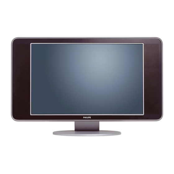
Colour Television
Contents
2. Safety and Maintenance Instructions,
Warnings, and Notes
I2C Overview
Rear IO Panel: PCHD-IO (23/26")(Diagram H2) 54
©
Copyright 2004 Philips Consumer Electronics B.V. Eindhoven, The Netherlands.
All rights reserved. No part of this publication may be reproduced, stored in a
retrieval system or transmitted, in any form or by any means, electronic,
mechanical, photocopying, or otherwise without the prior permission of Philips.
Published by BB 0466 Service PaCE
Page
2
5
7
8
11
19
20
21
22-23
24
25
Diagram PWB
(Diagram A1) 26
38-47
(Diagram A2) 27
38-47
(Diagram A3) 38
38-47
(Diagram A5) 29
38-47
(Diagram A6) 30
38-47
(Diagram A7) 31
38-47
(Diagram A9) 32
38-47
(Diagram A10) 33
38-47
(Diagram A11) 34
38-47
(Diagram A12) 35
38-47
(Diagram A13) 36
38-47
(Diagram A14) 37
38-47
(Diagram D)
48
49
(Diagram H1) 50
52
(Diagram H2) 51
52
(Diagram H1) 53
55
55
(Diagram J)
56
56
Printed in the Netherlands
Contents
Pixel Plus Panel: EPLD Control (Diagram PP1) 57
Pixel Plus Panel: Power Supply (Diagram PP4) 60
Subject to modification
Chassis
LC4.2E
AA
E_14490_000.eps
110604
Page
61
(Diagram PP2) 58
61
(Diagram PP3) 59
61
61
63
66
72
74
77
82
EN 3122 785 14491
Advertisement
Table of Contents

Related Manuals for Philips LC4.2E


Summary of Contents for Philips LC4.2E
-
Page 1: Table Of Contents
All rights reserved. No part of this publication may be reproduced, stored in a retrieval system or transmitted, in any form or by any means, electronic, mechanical, photocopying, or otherwise without the prior permission of Philips. Published by BB 0466 Service PaCE... -
Page 2: Technical Specifications, Connections, And Chassis Overview
EN 2 LC4.2E AA Technical Specifications, Connections, and Chassis Overview 1. Technical Specifications, Connections, and Chassis Overview : < 3 W Index of this chapter: - Standby 1. Technical Specifications 2. Connections Connections 3. Chassis Overview 1.2.1 Rear Connections Note: Figures below can deviate slightly from the actual situation, due to the different set executions. - Page 3 Technical Specifications, Connections, and Chassis Overview LC4.2E AA EN 3 External 2: RGB/YUV - In and CVBS - In/Out - SCL_DVI - SDA_DVI n.c. - RX1- 10 - RX1+ 11 - Ground E_06532_001.eps 050404 12 - n.c. 13 - n.c.
- Page 4 EN 4 LC4.2E AA Technical Specifications, Connections, and Chassis Overview LCD PANEL TV & SCALER BOARD PIXEL PLUS PANEL SIDE IO PANEL FRONT LED PANEL POWER SUPPLY UNIT REAR I/O CINCH PANEL E_14490_100.eps 040804 Figure 1-7 Chassis Overview...
- Page 5 Safety Instructions, Warnings, and Notes LC4.2E AA EN 5 2. Safety Instructions, Warnings, and Notes Safety Instructions voltages in the power supply section both in normal operation (G) and in standby (F). These values are indicated by means of the appropriate symbols.
- Page 6 Lead Free Solder Some PWBs in this chassis are “lead-free prepared”. This is indicated on the PWB by the PHILIPS lead-free logo (either by a service-printing or by a sticker). It does not mean that lead- free solder is actually used! Figure 2-2 Lead-free logo 2.3.5...
-
Page 7: Directions For Use
Directions for Use LC4.2E AA EN 7 3. Directions for Use You can download this information from the following website: http://www.philips.com/support... -
Page 8: Mechanical Instructions
EN 8 LC4.2E AA Mechanical Instructions 4. Mechanical Instructions Index of this chapter: 1. Service Position 2. Rear Cover Removal 3. Power Supply Unit Removal 4. TV & Scaler Board Removal 5. I/O Panel Removal 6. Side I/O & Keyboard Panel and Front LED Panel Removal 7. - Page 9 Mechanical Instructions LC4.2E AA EN 9 Rear Cover Removal TV & Scaler Board Removal E_14490_006.eps E_14490_004.eps 130404 130404 Figure 4-7 : TV & Scaler board shield removal Figure 4-5 Rear cover removal 1. Manually unlock and remove the top cover cap (5).
- Page 10 EN 10 LC4.2E AA Mechanical Instructions 1. Release the two clamps (1) at the I/O panel bracket. Exchanging the LCD Panel Carefully pull the bracket in the direction (2), as shown at the figure “I/O panel removal”, and remove it.
-
Page 11: Service Modes, Error Codes, And Faultfinding
Service Modes, Error Codes, and Fault Finding LC4.2E AA EN 11 5. Service Modes, Error Codes, and Fault Finding Index of this chapter: How to enter 1. Test Points To enter SDM, use one of the following methods: 2. Service Modes •... - Page 12 EN 12 LC4.2E AA Service Modes, Error Codes, and Fault Finding After entering SDM, the following screen is visible, with SDM in After entering SAM, the following screen is visible, with SAM in the upper right corner of the screen to indicate that the the upper right corner of the screen to indicate that the television is in Service Default Alignment Mode.
- Page 13 Service Modes, Error Codes, and Fault Finding LC4.2E AA EN 13 11. NVM Editor. Can be used to change the NVM data in the television set. See table “NVM data” further on. 12. SC NVM Editor. Can be used to edit Scaler NVM.
- Page 14 Introduction to highlight the PICTURE sub menu. 4. Press the MENU LEFT/RIGHT keys to enter the PICTURE ComPair (Computer Aided Repair) is a service tool for Philips sub menu. Consumer Electronics products. ComPair is a further 5. Use the MENU UP/DOWN keys to select SHARPNESS.
- Page 15 Service Modes, Error Codes, and Fault Finding LC4.2E AA EN 15 5.4.4 communicate (read and write) to devices on the I2C How To Order busses of the TV-set. • Manually (by asking questions to you): Automatic ComPair order codes (EU/AP/LATAM): diagnosis is only possible if the micro controller of the •...
-
Page 16: The Blinking Led Procedure
EN 16 LC4.2E AA Service Modes, Error Codes, and Fault Finding 5.7.2 If possible, check the entire contents of the error buffer. In Load default NVM values some situations, an error code is only the result of another error and not the actual cause of the problem (for example, a fault in In case a blank NVM is placed or when the NVM content is the protection detection circuitry can also lead to a protection). - Page 17 Service Modes, Error Codes, and Fault Finding LC4.2E AA EN 17 5.7.4 Video Processing No power 1. Check +12 V and 3V3 at position 1910. 2. If no supply, check the connector 1910. 3. If it is correct, check the power supply board.
- Page 18 EN 18 LC4.2E AA Service Modes, Error Codes, and Fault Finding Personal Notes: E_06532_012.eps 060804...
-
Page 19: Block Diagrams, Testpoint Overviews, And Waveforms
Block Diagrams, Testpoint Overviews, and Waveforms LC4.2E AA 6. Block Diagrams, Testpoint Overviews, and Waveforms Wiring Diagram Wiring Diagram 26" LVDS Connection Rigth Left LCD SCREEN Speaker Speaker LVDS CONNECTION INVERTER 1003 1200 1409 1910 1704 LVDS OUTPUT 1403 1002... -
Page 20: Block Diagram Tuner And If Video
Block Diagrams, Testpoint Overviews, and Waveforms LC4.2E AA Block Diagram Tuner and IF Video HERCULES SYSTEM 7011 TUNER +VIF HISTOGRAM PAL-MULTI/SECAM TDA12021 NTSC TDA12001 +VTUN CHINA/NTSC-AP TDA12011 +5VSW 7011 - IF 7014 1328 2321 VIF1 4327 1302 F306 R_SDTV Input... -
Page 21: Block Diagram Scaler
Block Diagrams, Testpoint Overviews, and Waveforms LC4.2E AA Block Diagram Scaler SCALER FLASH/CONTROL +3V3_IO 7607 +3V3STBY 7531 ADDRESS HERCULES PCHD-MUX SCREEN SIZE SDM PINS SD_HD_SEL SDTV HDTV 4022 PC_HD_SEL ENABLE DISABLE 7532 PRESENT ONLY FOR 23" 7011 PRESENT ONLY FOR 26"... -
Page 22: Testpoint Overview Tv & Scaler Board
Block Diagrams, Testpoint Overviews, and Waveforms LC4.2E AA Testpoint Overview TV & Scaler Board (Bottom Side) F001 B4 F018 C4 F032 C3 F046 D3 F061 D5 F090 C3 F309 B2 F406 A8 F461 C7 F534 C5 F602 C6 F619 C7... - Page 23 Block Diagrams, Testpoint Overviews, and Waveforms LC4.2E AA Testpoint Overview TV & Scaler Board (Top Side) ersonal Notes: SERVICE TESTPOINT F452 500mV / div DC 20us / div E_14490_022.eps 3139 123 5804.2 030604 E_06532_012.eps 130204...
- Page 24 Block Diagrams, Testpoint Overviews, and Waveforms LC4.2E AA I2C IC Overview I2C BUS INTERCONNECTION DIAGRAM HERCULES TUNER IF HISTOGRAM SCALER FLASH/CONTROL +3V3STBY +3V3STBY 3096 3088 F303 7011 +3V3STBY +3V3STBY PROCESSOR 3433 3432 PART OF VIDEO- F302 PROCESSER 3303 3302 (HERCULES) +3.3V...
-
Page 25: Supply Voltage Overview
Block Diagrams, Testpoint Overviews, and Waveforms LC4.2E AA Supply Voltage Overview TV SUPPLY TUNER IF PIXEL+ PANEL SUPPLY SCALER INTERFACE PANEL +3V3STBY 1409 1001 +3V3STBY 1200 1910 +5VSW 7504 F903 +3V3 +5VSW +5VSWI AUD_SUP AUD_SUP +5VSWI +VTUN 7501 +VTUN +3V3_PLL... -
Page 26: Circuit Diagrams And Pwb Layouts
Circuit Diagrams and PWB Layouts LC4.2E AA 7. Circuit Diagrams and PWB Layouts TV & Scaler Board: Tuner + VIF TUNER + VIF 1302 A1 F310 F9 1303 B1 F311 C1 1304 F1 F312 E2 1305 F1 F313 F2 1328-A B8... -
Page 27: Hercules
Circuit Diagrams and PWB Layouts LC4.2E AA TV & Scaler Board: Hercules 1001 C4 3006 D4 6073 B2 I054 E9 1002 F1 3007 D4 6074 B2 I055 E9 1009 G3 3008 E3 6075 B2 I056 F7 2001 D3 3009 G7... -
Page 28: Histogram
Circuit Diagrams and PWB Layouts LC4.2E AA TV & Scaler Board: Histogram 1004 G1 3562 D5 F093 G1 1005 A1 3563 D5 F094 G1 1008 D1 3564 D5 F095 G1 HISTOGRAM I341 I344 2019 A9 3565 D4 F096 G1 2020 A7... -
Page 29: Audio Amplifier
Circuit Diagrams and PWB Layouts LC4.2E AA TV & Scaler Board: Audio Amplifier 1701 A6 7706-4 F2 1704 D9 7707 A5 2701 A6 7708-1 F5 HPIC_LIN 2702 A4 7708-2 F5 AUDIO AMPLIFIER HPIC_RIN 2703 D5 7709 D6 +3V3STBY 4704 2704 A2... -
Page 30: Tv-Supply
Circuit Diagrams and PWB Layouts LC4.2E AA TV & Scaler Board: TV-Supply 1910 A1 TV-SUPPLY 2909 B3 2910 E8 2911 D9 2920 E4 11V9 2921 E5 F903 11V2 AUD-SUP 2930 C3 2931 C6 2936 2932 C4 1910 F904 2933 D6... -
Page 31: Scaler
Circuit Diagrams and PWB Layouts LC4.2E AA TV & Scaler Board: Scaler 1401 C3 I436 F2 1403 H16 I437 F2 1408 J15 I438 J11 SCALER 2457 G1 I439 K4 2487 C3 I440 K4 2488 C2 I441 I4 +1V8_CORE +3V3_IO +3V3_LBADC +2V5_DDR... -
Page 32: Scaler Interface
Circuit Diagrams and PWB Layouts LC4.2E AA TV & Scaler Board: Scaler Interface SCALER INTERFACE 1406 C4 2470 A5 1407 D4 2471 A6 1409 E4 2472 A6 +3V3_LVDS 2401 B1 2473 A6 +3V3_ADC +3V3_DVI +3V3_IO +3V3_LVDSA +3V3_LVDSB 2402 B1 2474 A6... -
Page 33: Sdram
Circuit Diagrams and PWB Layouts LC4.2E AA TV & Scaler Board: SDRAM 2501 E 2502 E 2503 E SDRAM +2V5_DDR 2504 E 2505 E 2506 E 3501 2507 E FSDATA0 2508 E FSVREF 2509 E FSVREF FSCLK+ F501 FSDATA1 I503... -
Page 34: Flash / Control
Circuit Diagrams and PWB Layouts LC4.2E AA TV & Scaler Board: Flash / Control FLASH / CONTROL 1530 C7 1532 E4 2530 A3 2531 D2 Resistor Item No 2532 D4 +3V3_IO Model & PANEL SIZE 3550 3553 3552 3551 3549... -
Page 35: Hdmi
Circuit Diagrams and PWB Layouts LC4.2E AA TV & Scaler Board: HDMI 1801 E1 2808 A8 2814 A7 2820 B7 2826 B7 2833 E11 2839 F3 2845 G11 3801-2 A11 3802-4 B11 3804-2 C11 3805-4 D11 3808 B2 3813-4 F9... -
Page 36: Pchd-Mux
Circuit Diagrams and PWB Layouts LC4.2E AA TV & Scaler Board: PCHD-MUX 1601 B1 6640 G4 2601 A7 6646 F2 2602 D5 7601 A7 2603 D6 7604-1 E6 PCHD-MUX 2604 D6 7604-2 E7 2605 E7 7604-3 E6 2606 E5 7604-4 F7... -
Page 37: Supply
Circuit Diagrams and PWB Layouts LC4.2E AA TV & Scaler Board: Supply 1951 C2 2953 G3 2954 G3 SUPPLY 2955 G4 2956 F5 2957 G6 2958 G6 2959 C5 2960 C6 2961 D4 2962 B6 +12VSW 2964 A3 2970 2965 B3... - Page 38 Circuit Diagrams and PWB Layouts LC4.2E AA Layout TV & Scaler Board: (Overview Top Side) 1002 C5 1409 A8 2011 B3 2028 A4 2055 B4 2082 B3 2317 D2 2371 C3 2405 B6 2421 C7 2437 B6 2452 C6 2471 C6...
- Page 39 Circuit Diagrams and PWB Layouts LC4.2E AA Layout TV & Scaler Board: (Part 1 Top Side) Part 1 E_14490_019a.eps 230404...
- Page 40 Circuit Diagrams and PWB Layouts LC4.2E AA Layout TV & Scaler Board: (Part 2 Top Side) Part 2 E_14490_019b.eps 230404...
- Page 41 Circuit Diagrams and PWB Layouts LC4.2E AA Layout TV & Scaler Board: (Part 3 Top Side) E_14490_019c.eps Part 3 230404...
- Page 42 Circuit Diagrams and PWB Layouts LC4.2E AA Layout TV & Scaler Board: (Part 4 Top Side) E_14490_019d.eps Part 4 230404...
- Page 43 Circuit Diagrams and PWB Layouts LC4.2E AA Layout TV & Scaler Board: (Overview Bottom Side) 1001 B6 2027 C5 2309 C6 2392 A6 2465 C3 2563 B5 2708 A6 2810 D1 2834 D2 2865 B2 2932 A5 2960 A3 3019 B5...
- Page 44 Circuit Diagrams and PWB Layouts LC4.2E AA Layout TV & Scaler Board: (Part 1 Bottom Side) Part 1 E_14490_020a.eps 230404...
- Page 45 Circuit Diagrams and PWB Layouts LC4.2E AA Layout TV & Scaler Board: (Part 2 Bottom Side) Part 2 E_14490_020b.eps 230404...
- Page 46 Circuit Diagrams and PWB Layouts LC4.2E AA Layout TV & Scaler Board: (Part 3 Bottom Side) Part 3 E_14490_020c.eps 230404...
- Page 47 Circuit Diagrams and PWB Layouts LC4.2E AA Layout TV & Scaler Board: (Part 4 Bottom Side) Part 4 E_14490_020d.eps 230404...
-
Page 48: Side Io And Lkb Panel
Circuit Diagrams and PWB Layouts LC4.2E AA Side IO and LKB Panel SIDE IO & LKB 1301 D4 S303 E8 1302 B1 S304 E8 1303 A5 S305 F6 1306 F8 S306 F6 1307 B9 S307 F7 +3V3_STBY 1308 E9 S308 F7... - Page 49 Circuit Diagrams and PWB Layouts LC4.2E AA Layout Side IO and LKB Panel (Top Side) Layout Side IO and LKB Panel (Bottom Side) 1301 A1 2301 A2 4329 B2 1302 B1 2302 A2 4330 A2 1303 B2 2303 A2 4331 A1...
-
Page 50: Rear Io Panel: Scart (17")
Circuit Diagrams and PWB Layouts LC4.2E AA Rear IO Panel: Scart (17”) 1101 A2 7138 C9 S130 C11 1102 A11 F101 A3 S131 C11 1103 C7 F103 B3 S132 C11 1104 E12 F105 B3 S133 C10 REAR IO SCART 1105 G2... -
Page 51: Rear Io Panel: Pchd-Io (17")
Circuit Diagrams and PWB Layouts LC4.2E AA Rear IO Panel: PCHD-IO (17”) PCHD-IO 1680-1 C1 I701 F2 1680-2 D1 I702 F2 1680-3 E1 I703 A2 2683 1687 A1 I704 A3 5683 1688 F1 I705 A3 1687 3683 I682 1698 B9... - Page 52 Circuit Diagrams and PWB Layouts LC4.2E AA Layout Rear IO Panel (17”) (Top Side) 1101 A2 1105 A6 1688 A10 2106 A1 2128 A3 2133 A4 2147 A6 2683 A7 2694 A7 2703 A8 3128 A3 3134 A4 3138 A3...
-
Page 53: Rear Io Panel: Scart (23/26")
Circuit Diagrams and PWB Layouts LC4.2E AA Rear IO Panel: Scart (23”/26”) 1101 A1 F101 A2 S127 A11 REAR IO SCART 1102 A12 F103 A2 S128 A11 1103 C7 F105 A2 S129 B11 1104 E12 F106 A2 S130 B11 1105 G2... - Page 54 Circuit Diagrams and PWB Layouts LC4.2E AA Rear IO Panel: PCHD-IO (23”/26”) 1687 A1 I706 E9 1688 E1 I709 C9 1698 B9 I710 A6 2681 C6 I711 E1 PCHD-IO 2683 A6 S698 E2 2684 A6 S699 E2 2686 C6 I710...
- Page 55 Circuit Diagrams and PWB Layouts LC4.2E AA Layout Rear IO Panel (23”/26”) (Top Side) 1101 A2 1105 A6 1698 A5 2107 A2 2129 A4 2134 A4 2148 A6 2684 A7 2694 A4 3132 A4 3136 A4 3140 A3 3155 A5...
-
Page 56: Front Ir / Led Panel
Circuit Diagrams and PWB Layouts LC4.2E AA Front IR / LED Panel Layout Front IR / LED Panel (Top Side) 1540 A1 2540 A1 6540 A1 6541 A1 7543 A1 1540 B1 2540 C4 2541 D2 3540 A3 3542 B4... - Page 57 Circuit Diagrams and PWB Layouts LC4.2E AA Pixel Plus Panel: EPLD Control 1100 B10 1101 F11 1102 F11 EPLD CONTROL 2101 B9 2102 B8 2103 C9 2104 C11 2105 C1 2106 C9 2107 D2 2108 D3 2110 E3 2112 F3...
-
Page 58: Pixel Plus Panel: Lvds In
Circuit Diagrams and PWB Layouts LC4.2E AA Pixel Plus Panel: LVDS In 1002 C1 1207 C4 1210 D4 2201 B8 2203 B8 2205 B7 2207 C3 2209 E2 2211 E3 2213 E3 2215 E3 3202 B6 3207 C4 3213 D4... -
Page 59: Pixel Plus Panel: Epld I/O
Circuit Diagrams and PWB Layouts LC4.2E AA Pixel Plus Panel: EPLD I/O 1003 D11 1403 D10 1404 E10 1405 F10 EPLD I/O 1406 G10 1407 C10 2401 B8 2402 B8 2403 B8 2404 B9 2405 B9 2406 D10 2407 D10... -
Page 60: Power Supply
Circuit Diagrams and PWB Layouts LC4.2E AA Pixel Plus Panel: Power Supply 1001 D1 2502 B3 2503 C6 2504 C6 POWER SUPPLY 2505 C7 2508 D3 2509 D3 2515 C3 2516 D4 2520 D3 2522 C5 3510 C3 3512 C5... - Page 61 Circuit Diagrams and PWB Layouts LC4.2E AA Layout Pixel Plus Panel (Top Side) Layout Pixel Plus Panel (Bottom Side) 1206 C1 2403 B1 3520 D1 1001 D1 1207 C1 2404 A1 4501 D1 1002 C1 1209 C1 2405 A1 5101 B1...
- Page 62 Circuit Diagrams and PWB Layouts LC4.2E AA ersonal Notes: E_06532_013.eps 200204...
-
Page 63: Alignments
Alignments LC4.2E AA EN 63 8. Alignments General: The Service Default Mode (SDM) and Service Hardware Alignments Alignment Mode (SAM) are described in chapter 5. Menu navigation is done with the cursor Up, Down, Left or Right keys There are no hardware alignments foreseen for the LCD-TV. - Page 64 (no offset difference). Then the offset values for the Delta Cool Equipment and setting and Delta Warm mode can be selected. Note that the • E.g. Fluke 54200 or Philips PM5580. alignment values are non-linear. The range is: -50 to +50, 0 • 100% “8-step grey scale” pattern.
- Page 65 Alignments LC4.2E AA EN 65 8.3.5 Sound How to change an Option Byte An Option Byte represents a number of different options. Changing these bytes directly makes it possible to set all No adjustments needed for sound. options very fast. All options are controlled via seven option bytes.
-
Page 66: Circuit Descriptions
EN 66 LC4.2E AA Circuit Descriptions, Abbreviation List, and IC Data Sheets 9. Circuit Descriptions, Abbreviation List, and IC Data Sheets • Index of this chapter Audio: The sound processor is part of the UOC processor 1. Introduction (called “Hercules”). The chassis has a FM Radio with 40 2. - Page 67 DVI-D in: This input is directly going to the Scaler IC. See paragraph “Video: Scaler Part”. Tuner and IF A Philips UR13xx Tuner with second input (for FM Radio) is used in the TV board. The SIF and FM signals are decoded by the Hercules. Tuning is done via I2C.
- Page 68 EN 68 LC4.2E AA Circuit Descriptions, Abbreviation List, and IC Data Sheets Video: TV Part (diagrams A1, A2, and A3) SYSTEM 7011 PAL-MULTI/SECAM TDA12021 NTSC TDA12001 +VTUN CHINA/NTSC-AP TDA12011 +5VSW 7011 - IF 7014 1328 2321 VIF1 4327 1302 R_SDTV...
- Page 69 Circuit Descriptions, Abbreviation List, and IC Data Sheets LC4.2E AA EN 69 7011 u-Processor 7605 7604 H_CS_SDTV R_SDTV H_CS V_SDTV G_SDTV B_SDTV 9,11 SD_HD_SEL HERCULES 7530 7607 ADDRESS R_SDTV EXT. G_SDTV FLASH FLASH R_PR+ B_SDTV INTER- H_CS_SDTV RED_PR G_Y+ ANALOG...
- Page 70 9.9.4 Audio: Lip Sync • It is used for all FM demodulation in AV-Stereo sets. The LC4.2E is not equipped with Lip Sync. This is not needed. 9.9.1 Diversity 9.10 Control The diversity for the Audio decoding can be broken up into two main concepts: •...
-
Page 71: Lcd Display
Circuit Descriptions, Abbreviation List, and IC Data Sheets LC4.2E AA EN 71 • LED. This signal is used as an indication for the Standby, Remote and Error Indicator. Region diversity: – During protection mode, the LED blinks and the set is in standby mode. -
Page 72: Abbreviation List
C-FRONT Chrominance front input LATAM LATin AMerica Circuit Board Assembly (or PWB) LC04 Philips chassis name for LCD TV 2004 Constant Level: audio output to project connect with an external amplifier Liquid Crystal Display CLUT Colour Look Up Table... - Page 73 Circuit Descriptions, Abbreviation List, and IC Data Sheets LC4.2E AA EN 73 Colour carrier NTSC M/N = 3.579545 S/PDIF Sony Philips Digital InterFace MHz, NTSC 4.43 = 4.433619 MHz SRAM Static RAM (this is a VCR norm, it is not...
-
Page 74: Ic Data Sheets
EN 74 LC4.2E AA Circuit Descriptions, Abbreviation List, and IC Data Sheets 9.13 IC Data Sheets This section shows the internal block diagrams and pin layouts of ICs that are drawn as "black boxes" in the electrical diagrams (with the exception of "memory" and "logic" ICs). -
Page 75: Pin Configuration
Circuit Descriptions, Abbreviation List, and IC Data Sheets LC4.2E AA EN 75 9.13.2 Diagram A7, Type GM1501 (IC7401) Block Diagram Parallel 2-wire IF/external Serial I/F JTAG GPIO micro Infra-red Rx Pulse Width Interface X186 External ndwid Modulator Micro- ROM I/F... - Page 76 EN 76 LC4.2E AA Circuit Descriptions, Abbreviation List, and IC Data Sheets 9.13.3 Diagram A12, Type S9993CT (IC7808) BLOCK DIAGRAM RESET# CSDA Registers Slave CSCL DSDA ---------------- Slave Configuration DSCL Logic Block Aux Data Logic HDCP HDCP Block MCLK Keys...
-
Page 77: Spare Parts List
Spare Parts List LC4.2E AA EN 77 10. Spare Parts List Set Level 2079 2020 552 96632 22nF 10% 16V 0402 2441 3198 035 71040 100nF 10% 16V 0402 2082 2020 552 96618 1nF 10% 50V 0402 2442 3198 035 71040 100nF 10% 16V 0402... - Page 78 EN 78 LC4.2E AA Spare Parts List 2617 2020 552 96628 10nF 10% 16V 0402 3321 4822 051 30222 2.2kΩ 5% 0.062W 2618 2020 552 96628 10nF 10% 16V 0402 3322 4822 051 30682 6.8Ω 5% 0.062W 2619 4822 126 14324 33pF 5% 50V 0402 3323 4822 051 30222 2.2kΩ...
- Page 79 Spare Parts List LC4.2E AA EN 79 3615 3198 031 02290 22Ω 5% 0.1W 0402 5372 2422 549 44197 Bead 220Ω at 100MHz 7605 4822 209 60792 74HC4053D 3616 3198 031 02290 22Ω 5% 0.1W 0402 5530 2422 549 45333 Bead 120Ω 100MHz...
- Page 80 EN 80 LC4.2E AA Spare Parts List 3143 4822 051 30759 75Ω 5% 0.062W 1002 2422 025 18314 Connector 20p m v 1.25 3152 4822 117 12891 220kΩ 1% 1003 2422 025 18314 Connector 20p m v 1.25 3153 4822 051 30151 150Ω 5% 0.062W 1206 2422 549 45325 Bead 67Ω...
- Page 81 Spare Parts List LC4.2E AA EN 81 2522 5322 126 11583 10nF 10% 50V 0603 3101 4822 051 30103 10kΩ 5% 0.062W 3102 4822 051 30479 47Ω 5% 0.062W 3103 4822 051 30479 47Ω 5% 0.062W 3104 4822 051 30103 10kΩ 5% 0.062W 3105 4822 051 30103 10kΩ...
-
Page 82: Revision List
EN 82 LC4.2E AA Revision List 11. Revision List Manual xxxx xxx xxxx.0 • First release. Manual xxxx xxx xxxx.1 The manual is updated with information for models with Pixel Plus. This information is only applicable for xxPF9956 models. •...
Need help?
Do you have a question about the LC4.2E and is the answer not in the manual?
Questions and answers