Table of Contents
Advertisement
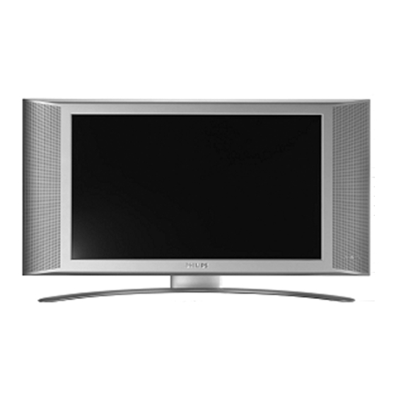
Colour Television
Contents
1
2
3
4
5
6
7
Electrical Diagrams and PWB lay-outs
TV Board: U_Cont
TV Board: Mem for 100-pg Txt (Diagram A2)
©
Copyright 2003 Philips Consumer Electronics B.V. Eindhoven, The Netherlands.
All rights reserved. No part of this publication may be reproduced, stored in a
retrieval system or transmitted, in any form or by any means, electronic,
mechanical, photocopying, or otherwise without the prior permission of Philips.
Published by RB 0370 Service PaCE
Page
2
5
6
14
20
27
29
30
31
32
33
34
35
36
37
Diagram PWB
(Diagram A1)
38
50-69
39
50-69
40
50-69
41
50-69
42
50-69
43
50-69
(Diagram A7)
44
50-69
(Diagram A8)
45
50-69
50-69
50-69
(Diagram A10) 48
50-69
(Diagram A11) 49
50-69
(Diagram C1)
70
80-89
(Diagram C2)
71
80-89
Printed in the Netherlands
Contents
8
9
Subject to modification
Chassis
LC03E
AA
Page
(Diagram C3)
72
80-89
73
80-89
(Diagram C5)
74
80-89
75
80-89
76
80-89
(Diagram C8)
77
80-89
78
80-89
80-89
90
91
90
92
(Diagram IN)
93
94
(Diagram IN1) 95
97
(Diagram IN2) 96
97
98
98
99
103
115
117
120
126
EN 3122 785 13571
Advertisement
Table of Contents

Related Manuals for Philips LC03E


Summary of Contents for Philips LC03E
-
Page 1: Table Of Contents
All rights reserved. No part of this publication may be reproduced, stored in a retrieval system or transmitted, in any form or by any means, electronic, mechanical, photocopying, or otherwise without the prior permission of Philips. Published by RB 0370 Service PaCE... -
Page 2: Technical Specifications, Connections, And Chassis Overview
Technical Specifications, Connections, and Chassis Overview EN 2 LC03E 1. Technical Specifications, Connections, and Chassis Overview : 1 W Technical Specifications Standby Power dissipation : 15”: 6.2 kg Weight : 17”: 6.4 kg 1.1.1 Reception : 23”: 11.5 kg : 517 x 307 x 65 mm Dim. - Page 3 Technical Specifications, Connections, and Chassis Overview LC03E EN 3 1.2.4 SCART EXT/2 (CVBS +YC) Only for 17’’ and 23” models Rear Connections Part 3 CL96532137_056.eps 171199 DC In Audio In (PC) EXT. 1 PC Input (VGA) FM ANT Figure 1-3 SCART connector CL 36532054_020.eps...
- Page 4 Technical Specifications, Connections, and Chassis Overview EN 4 LC03E 7 - Blue 0.7 V_pp/75 ohm 15 - Red 0.7 V_pp/75 ohm 8 - CVBS-status 0 - 1.3 V: INT 16 - RGB-status/ 4.5 - 7 V: EXT 16:9 0 - 0.4 V: INT 9.5 - 12 V: EXT 4:3...
-
Page 5: Safety Instructions, Warnings, And Notes
Safety Instructions, Warnings, and Notes LC03E EN 5 2. Safety Instructions, Warnings, and Notes • Safety Instructions Capacitor values may also use the value multiplier as the decimal point indication (e.g. 2p2 indicates 2.2 pF). • An 'asterisk' (*) indicates component usage varies. Refer to Safety regulations require that during a repair: the diversity tables for the correct values. -
Page 6: Directions For Use
Directions for Use EN 6 LC03E 3. Directions for Use... - Page 7 Directions for Use LC03E EN 7...
- Page 8 Directions for Use EN 8 LC03E...
- Page 9 Directions for Use LC03E EN 9...
- Page 10 Directions for Use EN 10 LC03E...
- Page 11 Directions for Use LC03E EN 11...
- Page 12 Directions for Use EN 12 LC03E...
- Page 13 Directions for Use LC03E EN 13...
-
Page 14: Mechanical Instructions
Mechanical Instructions EN 14 LC03E 4. Mechanical Instructions Index of this chapter: 1. Service Position 2. Stand Removal 3. Rear Cover Removal 4. Shield Removal 5. I/O Assy Removal 6. LED/Remote Control Board Removal 7. TV Board Removal 8. Scaler Board Removal 9. - Page 15 Mechanical Instructions LC03E EN 15 Continue with the paragraph 4.3.3. VGA connector distance screws 4.3.2 For 23 inch model Manually unlock and remove the IO connector cover cap. Connector cover cap CL 36532044_006.eps 160503 Figure 4-8 VGA Connector screws •...
- Page 16 Mechanical Instructions EN 16 LC03E 2. To completely remove the Front LED panel (incl. Lens), I/O Removal remove the assy screw. 4.5.1 Side I/O assy removal for 15/17 inch model TV Board Removal 4.7.1 For 15 /17inch model Disconnect all five TV board connectors out of the regarding sockets [3225], [1234], [1231], [1902], and [1732].
- Page 17 Mechanical Instructions LC03E EN 17 Scaler Board Removal 1. Carefully disconnect the cable connector in the centre of the Scaler board [1506]. Take care not to damage the fragile cables. 2. Disconnect the cable connectors at the edge of the Scaler board [1402] and [1003].
-
Page 18: Lcd Panel Removal
Mechanical Instructions EN 18 LC03E Mounting screw(2x) CL 36532044_015.eps 160503 Figure 4-19 Top control assy CL 36532044_016.eps 4.11 LCD Panel Removal 160503 4.11.1 For 15 /17 inch model Figure 4-21 LCD frame mounting screws 23” model 4.11.3 For all models Note: the LCD Panel is available in two versions: a TN-display and an IPS-display. - Page 19 Mechanical Instructions LC03E EN 19 of the bottom side. You will need this screw position for mounting the TV rear cover. • Take extra care when fixing the connector bracket screw at SCART plug side. You can easily damage the TV board when you use too much force.
-
Page 20: Service Modes, Error Messages, And Repair Tips
Service Modes, Error Messages, and Repair Tips EN 20 LC03E 5. Service Modes, Error Messages, and Repair Tips Index of this chapter: 1. Test Points For recognition, “SDM” is displayed at the upper right corner of 2. Service Modes the screen. - Page 21 Service Modes, Error Messages, and Repair Tips LC03E EN 21 • Access to SAM Change the value of the selected menu item (e.g. By pressing 0-6-2-5-9-6 “info+” (or OSD) in sequence on the HOR.SHIFT). • standard RC will switch from SDM to SAM.
- Page 22 Service Modes, Error Messages, and Repair Tips EN 22 LC03E 1. Select ”FEATURE” menu (with the Remote Control) 2. Select “LOCK” (with the RC) T Y P E : 1 7 P F 9 9 4 5 / 0 1 2...
- Page 23 Service Modes, Error Messages, and Repair Tips LC03E EN 23 The contents of the error buffer can also be made visible TV-Board through the “blinking LED” procedure. This is especially useful when there is no picture. See paragraph 5.4 “The blinking LED Errors procedure “.
- Page 24 If the core supply voltage is too low or data line is ComPair (Computer Aided Repair) is a service tool for Philips broken, this error protection will be activated. Under these Consumer Electronics products.
- Page 25 Service Modes, Error Messages, and Repair Tips LC03E EN 25 5.5.3 How To Connect Trouble Shooting Tips 1. First, install the ComPair Browser software (see the Quick 5.6.1 Scaler/TV Board Power Supply Problems Reference Card for installation instructions). 2. Connect the RS232 interface cable between a free serial...
- Page 26 Service Modes, Error Messages, and Repair Tips EN 26 LC03E 5.6.2 5. Select the STORE menu item General Problems • When the set is in PC mode and there is no VGA signal present at PC-in connector, the set will shutdown to TV switched “off”...
-
Page 27: Block Diagrams
Block Diagrams, Testpoint Overviews, and Wiring Diagram LC03E 6. Block Diagrams, Testpoint Overviews, and Wiring Diagram Block Diagram (Tuner-IF-Video) TUNER +5V4 VIDEO & QSS IF VDP - COLOUR PROCESSING VDP - COLOUR PROCESSING ANALOG COMB FILTER C-SYNC GENERATOR +8V3A MAIN-CBVS-EXT-IN... -
Page 28: Block Diagram (Tv Control And Inverter Panel)
Block Diagrams, Testpoint Overviews, and Wiring Diagram LC03E Block Diagram (TV Control and Inverter Panel) CONTROLS +3V5 7066 7064 PC-TV-LED SDA-NVM HP-SIDE-DET (SCART) STATUS2_SVHS-RR-DET STATUS1 (SCART) HIS-OFF COMM-LINE 3029 KEYBOARD 7022 LIGHT-SENSOR_SDM SEL-MAIN-FRNT-RR PC-HDAUDIO-L A(14) SOUND-ENABLE PC-HDAUDIO-R OENOT STAND-BY WENOT... -
Page 29: Block Diagram (Scaler Board)
Block Diagrams, Testpoint Overviews, and Wiring Diagram LC03E Block Diagram (Scaler Board) I/O & INTERFACE VIDEO DECODER OUTPUT (LVDS) VIDEO CONVERTER SCALER 7402-JagASM (NOT USED) 7501 1401 SOFT-RESET IICSDA TXOUT0- PLL1 MEM CLK 1301 +3V3 OSC GEN IICSCL TXOUT0+ IICSCL... -
Page 30: I2C-Ic's And Error Codes Overview
Block Diagrams, Testpoint Overviews, and Wiring Diagram LC03E I2C-IC’s and Error Codes Overview TUNER IF-VIDEO AUDIO COMB PROCESSING FILTER +3V5 +3V5 3048 3047 1426 1801 3085 CONNECTION SDA-0 3017 3D COMB SCL-0 FILTER (OPTIONAL) 3101 3100 3332 3331 3621 3620... -
Page 31: Powerlines Overview
Block Diagrams, Testpoint Overviews, and Wiring Diagram LC03E Powerlines Overview 1003 POWER VIDEO DECODER INVERTER (FOR 15" AND 17" ONLY) LOCAL SUPPLY 1902 7301 12_24DC_SUP 5304 12_24DC_SUP K4-7302 5900 12_24DC_SUP-1 1002 12_24DC_SUP 1001-1 +3V3 +3V3 5901 7000mA SUPPLY 7920 UNIT... -
Page 32: Testpoint Overview Tv Board (15"/17")
Block Diagrams, Testpoint Overviews, and Wiring Diagram LC03E Testpoint Overview TV Board (15”/17”) CL 36532023_035.eps 3139 123 5592.4 061003... -
Page 33: Mapping Testp. And Waveforms Tv Board
Block Diagrams, Testpoint Overviews, and Wiring Diagram LC03E Mapping Testpoint Overview and Waveforms TV Board (15”/17”) Mapping Testpoint Overview and Waveforms Scaler Board F044 F385 F735 F008 = 5V DC F531 F691 F002 B4 F428 C6 F001 A7 I014 I304... -
Page 34: Testpoint Overview Scaler Board
Block Diagrams, Testpoint Overviews, and Wiring Diagram LC03E Testpoint Overview Scaler Board CL 36532023_036.eps 3139 123 5680.3 061003... -
Page 35: Testpoint Overview Tv Board (23")
Block Diagrams, Testpoint Overviews, and Wiring Diagram LC03E Testpoint Overview TV Board (23”) F002 B4 F008 B5 F014 C5 F044 C4 F068 C4 F074 A5 F085 A4 F105 A8 F201 B8 F206 C8 F211 D7 F216 D6 F222 D5 F227 D5... -
Page 36: Wiring Diagram 15 & 17 Inch
Block Diagrams, Testpoint Overviews, and Wiring Diagram LC03E Wiring Diagram (15”/17”) Wiring Diagram 15" & 17"WS Top Control Panel 1500_4P LCD PANEL TO LCD PANEL TV Board Inverter Panel Right Left Scaler Board CN3_2P CN2_2P Speaker Speaker Side I/O Panel... -
Page 37: Wiring Diagram23 Inch Wide Screen
Block Diagrams, Testpoint Overviews, and Wiring Diagram LC03E Wiring Diagram23 Inch Wide Screen Wiring Diagram 23"WS Top Control Panel 1500_4P LCD PANEL Side I/O Panel 0240_11P TO LCD PANEL TV Board Scaler Board Right Speaker Left Speaker 1506_40P 1111_3P Front LED... - Page 38 Circuit Diagrams and PWB Layouts LC03E 7. Circuit Diagrams and PWB Layouts TV Board: U_Cont U_CONT (COMMON) FOR DIVERSITY TABLE SEE DIAGRAM A2 1010 C1 3071 E2 1057 E7 3072 E1 2010 B4 3081 E3 2012 E3 3082 E3 +3V5...
- Page 39 Circuit Diagrams and PWB Layouts LC03E TV Board: Memory for 100-pg Teletext Personal Notes: 2060 A1 MEMORY FOR 100-PG TELETEXT 2061 A2 (COMMON FOR EUROPE & AP-PAL) 5050 A2 7070 A2 +3V5 5050 2060 2061 100n 100n 7070 A(0) CY7C1019CV33...
-
Page 40: Tv Board: Tuner Function (Diagram A3)
Circuit Diagrams and PWB Layouts LC03E TV Board: Tuner Function TUNER FUNCTION (15"/17"/23" SCART) 1100 B2 1111 C1 2101 D3 2102 D3 2103 C5 2104 C4 2106 C5 2107 C6 DC/DC CONVERTER +5V4 2108 D5 Item# Component type 2120 A7... -
Page 41: Tv Board: If Video Sync Chr
Circuit Diagrams and PWB Layouts LC03E TV Board: IF Video Sync Chroma F355 F340 F341 F342 F346 F350 F352 F358 IF-VIDEO -SYNC-CHROMA (15"/17"/23" EUROPE, AP & LATAM ) 1V / div DC 1V / div DC 1V / div DC... -
Page 42: Tv Board: Saw Filter (Diagram A5)
Circuit Diagrams and PWB Layouts LC03E TV Board: SAW Filter, Ext. Video Select, Histogram, & C-Sync Generator F385 F413 F470 F471 F472 F480 SAW FILTER, EXT. VIDEO SELECT, HISTROGRAM & C-SYNC GEN (15"/17"/23" EUROPE & AP-PAL) 200mV / div DC... - Page 43 Circuit Diagrams and PWB Layouts LC03E TV Board: Analog Comb Filter ANALOG COMB FILTER (15"/17"/23" EUROPE, AP & LATAM) 1426 D1 2424 C1 2426 B1 +8V3A 2428 B1 Item# Component type 2429 C1 1426 ¥ CON BM V 10P M 2.50...
-
Page 44: Tv Board: Audio Delay Line
Circuit Diagrams and PWB Layouts LC03E TV Board: Audio Delay Line AUDIO DELAY LINE (COMMON) 2601 B2 2602 D2 2603 B2 2604 B7 2605 B8 2610 F6 2611 F6 2612 D9 5601 F601 2613 D9 +5V4 +5VD 3610 F5 3611 F6... -
Page 45: Tv Board: Audio Processing
Circuit Diagrams and PWB Layouts LC03E TV Board: Audio Processing AUDIO PROCESSING (COMMON) 1620 E7 2623 B1 2628 C2 2633 B2 2638 D2 2647 B1 2652 C8 2657 B7 2664 D8 2669 E7 2674 E9 2679 B7 2684 A3 3620 A2... -
Page 46: Tv Board: Audio Ampl. (15"/17")(Diagram A9A)
Circuit Diagrams and PWB Layouts LC03E TV Board: Audio Amplifier 2x3 Watts (15”/17”) 1232 A1 AUDIO AMPLIFIER 2x3 Watts 1702 A1 1730 A4 1731 A9 (15"/17") 1732 B9 1733 A4 1750 A7 1752 B7 1733 1731 FOR ITV 2731 D5... -
Page 47: Tv Board: Audio Amplifier (23") (Diagram A9B)
Circuit Diagrams and PWB Layouts LC03E TV Board: Audio Amplifier 2x5 Watts (23”) 1232 A1 F736 C8 1702 A2 F737 C8 AUDIO AMPLIFIER 2x5 Watts 1730 B3 F738 C8 1731 A9 F739 C8 (23") 1732 C9 F740 C2 1733 A4... -
Page 48: Tv Board: Local Supply
Circuit Diagrams and PWB Layouts LC03E TV Board: Local Supply 1902 C1 1903 C3 2900 C2 2903 F3 7910 LOCAL SUPPLY 2910 B4 MC34063A 2911 A7 8 DCOL 2912 B5 (COMMON) 11V7 2913 B7 2914 B5 2920 E4 7 IS... -
Page 49: Tv Board: Scart I/O
Circuit Diagrams and PWB Layouts LC03E TV Board: SCART I/O (15”/17”/23”) SCART IO (15"/17"/23" SCART) 1201 C7 3231 A7 F236 E7 1202 A3 3232 A8 F237 E7 1203 A3 3233 A7 F238 F7 1204 B3 3234 A8 SCART_1 SCART_2 (AP/TM/NA used 3291) -
Page 50: Tv Board: Analog Comb Filter (Diagram A6)
Circuit Diagrams and PWB Layouts LC03E Layout TV Board (15”/17”) (Overview Top Side) 1010 A4 1260 C1 1733 D5 2021 C5 2057 C5 2126 B3 2308 A3 2332 B4 2429 C3 2479 A5 2629 B6 2640 B6 2656 B7 2670 B7... - Page 51 Circuit Diagrams and PWB Layouts LC03E Layout TV Board (15”/17”) (Part 1 Top Side) Part 1 CL 36532023_33a.eps 110903...
- Page 52 Circuit Diagrams and PWB Layouts LC03E Layout TV Board (15”/17”) (Part 2 Top Side) Part 2 CL 36532023_33b.eps 110903...
- Page 53 Circuit Diagrams and PWB Layouts LC03E Layout TV Board (15”/17”) (Part 3 Top Side) Part 3 CL 36532023_33c.eps 110903...
- Page 54 Circuit Diagrams and PWB Layouts LC03E Layout TV Board (15”/17”) (Part 4 Top Side) Part 4 CL 36532023_33d.eps 110903...
- Page 55 Circuit Diagrams and PWB Layouts LC03E Layout TV Board (15”/17”) (Overview Bottom Side) 1201 D6 1214 D7 1270 D6 2054 C6 2203 C7 2244 D6 2314 B6 2340 A5 2381 A7 2431 C6 2605 B1 2751 D2 3012 B5 3047 B4...
- Page 56 Circuit Diagrams and PWB Layouts LC03E Layout TV Board (15”/17”) (Part 1 Bottom Side) Part 1 CL 36532023_34a.eps 110903...
- Page 57 Circuit Diagrams and PWB Layouts LC03E Layout TV Board (15”/17”) (Part 2 Bottom Side) Part 2 CL 36532023_34b.eps 110903...
- Page 58 Circuit Diagrams and PWB Layouts LC03E Layout TV Board (15”/17”) (Part 3 Bottom Side) Part 3 CL 36532023_34c.eps 110903...
- Page 59 Circuit Diagrams and PWB Layouts LC03E Layout TV Board (15”/17”) (Part 4 Bottom Side) Part 4 CL 36532023_34d.eps 110903...
- Page 60 Circuit Diagrams and PWB Layouts LC03E Layout TV Board (23”) (Overview Top Side) 1010 A4 1426 C3 2017 C4 2057 C5 2224 C2 2326 B3 2430 C3 2622 B5 2638 B6 2658 B7 2676 B6 2738 D7 2914 A8 3016 C4...
- Page 61 Circuit Diagrams and PWB Layouts LC03E Layout TV Board (23”) (Part 1 Top Side) Part 1 CL 36532054_01a.eps 240703...
- Page 62 Circuit Diagrams and PWB Layouts LC03E Layout TV Board (23”) (Part 2 Top Side) Part 2 CL 36532054_01b.eps 240703...
- Page 63 Circuit Diagrams and PWB Layouts LC03E Layout TV Board (23”) (Part 3 Top Side) Part 3 CL 36532054_01c.eps 240703...
- Page 64 Circuit Diagrams and PWB Layouts LC03E Layout TV Board (23”) (Part 4 Top Side) Part 4 CL 36532054_01d.eps 240703...
- Page 65 Circuit Diagrams and PWB Layouts LC03E Layout TV Board (23”) (Overview Bottom Side) 1201 D6 1217 D6 2014 C6 2132 B6 2244 D6 2320 A6 2346 A5 2407 C7 2605 B1 2759 D4 3017 B4 3061 C4 3103 B7 3213 C8...
- Page 66 Circuit Diagrams and PWB Layouts LC03E Layout TV Board (23”) (Part 1 Bottom Side) Part 1...
- Page 67 Circuit Diagrams and PWB Layouts LC03E Layout TV Board (23”) (Part 2 Bottom Side) Part 2 CL 36532054_02b.eps 240703...
- Page 68 Circuit Diagrams and PWB Layouts LC03E Layout TV Board (23”) (Part 3 Bottom Side) Part 3 CL 36532054_02c.eps 240703...
- Page 69 Circuit Diagrams and PWB Layouts LC03E Layout TV Board (23”) (Part 4 Bottom Side) Part 4 CL 36532054_02d.eps 240703...
-
Page 70: Scaler Panel: Power
Circuit Diagrams and PWB Layouts LC03E Scaler Panel: Power POWER 0121 F3 F001 A1 0122 F6 F002 A1 1001 A1 F003 A1 12-24DC-SUP 1002 A1 F005 B3 SS = 12V 1003 LS = 24V 1003 A2 F006 A2 1002 1001-1... -
Page 71: Scaler Panel: I/O & Interface
Circuit Diagrams and PWB Layouts LC03E Scaler Panel: I/O & Interface Personal Notes: I/O & INTERFACE 1681 A3 F681 A2 F682 A2 F683 A2 F684 B2 F685 B2 F686 B2 F687 B2 1681 F681 F688 B2 PC_HDAUDIO-L F689 C2 F690 C2... -
Page 72: Scaler Panel: Video Decoder
Circuit Diagrams and PWB Layouts LC03E Scaler Panel: Video Decoder VIDEO DECODER 1301 E5 2304 C2 2305 C2 +3V3 2308 C2 2315 D2 2316 D4 2321 5303 5302 5301 2317 D3 2318 D3 2319 D3 I302 I303 2331 2324 I301... -
Page 73: Scaler Panel: Scaler (Diagram C4)
Circuit Diagrams and PWB Layouts LC03E Scaler Panel: Scaler 1401 K6 F405 J7 1402 A9 I401 D8 2401 B2 I402 E8 2402 B2 I403 E8 SCALER 2403 B2 I404 E8 I405 A13 2404 B3 2405 C1 I406 C15 TO INVERTER PCB J1... -
Page 74: Scaler Panel: Output (Lvds)
Circuit Diagrams and PWB Layouts LC03E Scaler Panel: Output (LVDS) OUTPUT (LVDS) 1506 B9 2501 A7 2512 A7 5501 F537 +3V3 2513 A8 2516 B1 5512 F538 2517 B1 +3PLL 2518 B2 2521 E9 5513 LVDS F539 +3LVDS +3PLL +3V3... -
Page 75: Scaler Panel: Sdram (Scaler) (Diagram C6)
Circuit Diagrams and PWB Layouts LC03E Scaler Panel: SDRAM (Scaler) SDRAM (SCALER) 2471 A3 2472 A4 2474 A4 2475 A3 2476 A4 +3V3 +3V3 +3V3 +3V3 2477 A3 2478 A4 2480 A9 2481 A9 2482 A9 2483 A9 2484 A8... -
Page 76: Scaler Panel: Pc-In (Diagram C7)
Circuit Diagrams and PWB Layouts LC03E Scaler Panel: PC-In 1201 B8 I207 E4 2201 A7 I208 F8 2202 C11 I209 F7 2203 D5 I210 E4 PC-IN 2204 D6 2205 D6 2206 D4 2207 F5 BAS316 I200 2208 B9 2211 C9... -
Page 77: Scaler Panel: Up
Circuit Diagrams and PWB Layouts LC03E Scaler Panel: uP 1751 B1 I775 B4 1752 B6 I776 C7 +3V3 IICSDA 1753 A5 I777 C9 7751 2751 2751 A8 I778 C7 74LVC373APW 7752 2752 A4 I779 C9 M24C16 100n 2753 A5 I781 C7... -
Page 78: Scaler Panel: Video Converter (Diagram C9)
Circuit Diagrams and PWB Layouts LC03E Scaler Panel: Video Converter 1351 H2 I375 E12 1352 I5 I376 J12 2338 J14 I377 D11 2339 J14 I378 F12 VIDEO CONVERTER 2341 J13 I379 F12 2342 J13 I381 G12 2343 J14 I382 G12... -
Page 79: Scaler Panel: Hdtv Decoder (Diagram C10)
Circuit Diagrams and PWB Layouts LC03E Scaler Panel: HDTV Decoder HDTV - DECODER 1251 B1 6255 B2 1252 B2 6260 B2 1253 C2 6261 A2 1254 D2 7251 A2 1255 E2 7252 A6 1256 F2 F250 F3 5257 1283 E1... - Page 80 Circuit Diagrams and PWB Layouts LC03E Layout Scaler Panel (Overview Top Side) 0121 A5 1401 B2 2008 A7 2202 B1 2218 A1 2263 C1 2321 D7 2387 C5 2452 B2 3003 A7 3202 B2 3224 A1 3236 B1 3271 D2...
- Page 81 Circuit Diagrams and PWB Layouts LC03E Layout Scaler Panel (Part 1 Top Side) Part 1 CL 26532023_29a.eps 061003...
- Page 82 Circuit Diagrams and PWB Layouts LC03E Layout Scaler Panel (Part 2 Top Side) Part 2 CL 26532023_29b.eps 061003...
- Page 83 Circuit Diagrams and PWB Layouts LC03E Layout Scaler Panel (Part 3 Top Side) Part 3 CL 26532023_29c.eps 061003...
- Page 84 Circuit Diagrams and PWB Layouts LC03E Layout Scaler Panel (Part 4 Top Side) Part 4 CL 26532023_29a.eps 061003...
- Page 85 Circuit Diagrams and PWB Layouts LC03E Layout Scaler Panel (Overview Top Side) 1252 D7 2014 A6 2260 C6 2275 D7 2293 C7 2332 D2 2351 C3 2362 D5 2373 C4 2386 D3 2407 B4 2421 B5 2432 B5 2449 B5...
- Page 86 Circuit Diagrams and PWB Layouts LC03E Layout Scaler Panel (Part 1 Bottom Side) Part 1 CL 36532023_30a.eps 061003...
- Page 87 Circuit Diagrams and PWB Layouts LC03E Layout Scaler Panel (Part 2 Bottom Side) Part 2 CL 36532023_30b.eps 061003...
- Page 88 Circuit Diagrams and PWB Layouts LC03E Layout Scaler Panel (Part 3 Bottom Side) Part 3 CL 36532023_30c.eps 061003...
- Page 89 Circuit Diagrams and PWB Layouts LC03E Layout Scaler Panel (Part 4 Bottom Side) Part 4 CL 36532023_30d.eps 061003...
-
Page 90: Side I/O Panel (Diagram D)
Circuit Diagrams and PWB Layouts LC03E Side I/O Panel Top Control 0240 A4 1256-A A1 2297 E3 3292 C3 4202 A2 6297 A2 I208 C2 I218 B2 SG03 C2 1500 B1 0241 C4 1256-B A1 3285 A3 3293 C2 6291 E2... - Page 91 Circuit Diagrams and PWB Layouts LC03E Layout Side I/O Panel (Top Side) Layout Side I/O Panel (Bottom Side) 3292 B1 0240 C1 3294 C1 0241 A1 3296 D1 0242 A1 3297 D1 1254 D1 4201 B1 1255 C1 4202 A1...
- Page 92 Circuit Diagrams and PWB Layouts LC03E Layout Top Control (Top Side) 1500 A2 1501 A3 1502 A6 1503 A5 1504 A2 1505 A1 CL 36532023_025.eps 3139 123 5609.1 160503 Layout Top Control (Bottom Side) 2500 A4 3500 A4 3501 A2...
-
Page 93: Inverter Panel (Tn)
Circuit Diagrams and PWB Layouts LC03E Inverter Panel (TN) INVERTER PANEL (TN) T/ EFD20 TO BACK LIGHTS SI4425 330J/D IP SM 02B -B HSS-1-T B FROM/TO 100K F/4A /1206 1402 ON/ O F F 33uF 3904 33uF Vc om N15 N16... - Page 94 Circuit Diagrams and PWB Layouts LC03E Layout Inverter Panel (TN) C19 A6 CN5 B1 D33 A6 R13 A5 R27 C6 R39 A2 C30 A8 CP1 B5 D34 A6 R15 A5 R30 C8 R40 C6 C31 B8 CP2 A6 R17 A5...
-
Page 95: Inverter Panel (Ips)
Circuit Diagrams and PWB Layouts LC03E Inverter Panel (IPS) INVERTER PANEL (IPS) T/EEL19 20:1500 C/39p C/225K/1206 C/0 ohm/0805 VIN-1 R/100K/1206 NDR-B C/225K/1206 BHR-03VS-1 R/10K R/10K C/333K/0805 D/RLZ5.1B D/RLZ5.1B C/220uF U/4600 C/225K/1206 L/350m R/100K/1206 C/473K C/473K NDR-D PDR-A PDR-C C/333K/0805 R/100K/1206... -
Page 96: Inverter Panel (Ips)
Circuit Diagrams and PWB Layouts LC03E Inverter Panel (IPS) C17 C6 INVERTER PANEL (IPS) C19 C6 C20 A4 C29 A5 C37 A2 C/225K/1206 T/EEL19 20:1500 C/39pF C39 B2 VIN-2 C40 B5 C/0 ohm/0805 NDR-D C47 B5 C48 A1 C/225K/1206 BHR-03VS-1... - Page 97 Circuit Diagrams and PWB Layouts LC03E Layout Inverter Panel (IPS) (Top Side) C17 B3 C29 B2 C37 B3 C43 B6 C49 B5 C55 B2 CN2 B6 CP10 A3 CT1 B4 R13 A4 R30 A4 R49 B4 C19 B3 C39 B3...
-
Page 98: Front Led Panel (Diagram J)
Circuit Diagrams and PWB Layouts LC03E Front LED Panel Layout Front LED Panel (Top Side) 1170 B1 2177 C4 2180 D3 1170 A2 2177 A2 2180 A1 6175 A2 6176 A2 6177 A1 7178 A1 2181 D2 3171 B2 FRONT LED... -
Page 99: Electrical Alignments
Electrical Alignments LC03E EN 99 8. Electrical Alignments General: The Service Default Mode (SDM) and Service Hardware Alignments Alignment Mode (SAM) are described in chapter 5. Menu navigation is done with the CURSOR UP, DOWN, LEFT or There are no hardware alignments foreseen for the LCD-TV. - Page 100 EN 100 LC03E Electrical Alignments 8.3.2 8.3.4 Geometry Tuner Adjustment The geometry alignments menu contains 2 items to align a AGC (RF AGC Take Over Point) correct picture geometry. In wide screen sets, the GEOMETRY Set pattern generator (e.g. PM5418) with colour bar pattern...
- Page 101 VDBY ON=Enabled, menu item DOLBY VIRTUAL available. OFF=Disabled, ALPS compatible tuner is used. Philips Tuner PITN ON=Enabled, Philips compatible tuner is used. OFF=Disabled, Automatic Channel Installation. Automatic Channel Installation ON=Enabled Automatic Channel Installation. OFF=Disabled, automatic tuning system is ignored. Automatic Tuning System ON=Enabled Automatic tuning system, sort the program in an ascending order starting from Program 1.
- Page 102 EN 102 LC03E Electrical Alignments 8.4.3 Option bits/bytes (Default values) Table 8-3 Option bytes default values OB1 118 123 79 OB2 175 191 191 87 223 223 OB3 39 163 167 167 OB4 24 140 156 156 OB5 128 128 128 64...
-
Page 103: Circuit Descriptions
Circuit Descriptions, Abbreviation List, and IC Data Sheets LC03E EN 103 9. Circuit Descriptions, Abbreviation List, and IC Data Sheets 11. LCD Display Index of this chapter 1. Introduction 12. Abbreviation List 2. Block Diagram 13. IC Data Sheets 3. Power Supply 4. -
Page 104: Power Supply
EN 104 LC03E Circuit Descriptions, Abbreviation List, and IC Data Sheets The PLL tuner UR1316 (with FM radio) delivers the IF-signal, Power Supply via audio & video SAW-filters, to the multi-system TV processor TDA888x (item 7301, also called BOCMA). This IC has the... - Page 105 Tuner and IF 9.5.1 Tuner (diagram A3, A4, and A5) A Philips UR1336MK3 Tuner with second input (for FM Radio) is used in the TV board. The SIF FM signal is decoded by the Micronas IC. The tuner is I2C controlled, and is capable of receiving off-air, S- (cable) and Hyperband channels channels.
- Page 106 EN 106 LC03E Circuit Descriptions, Abbreviation List, and IC Data Sheets Video: TV-board (diagrams A4 and A5) 1454 VSIF 1100 TUNER 1452 STATUS1_PIP- 7301 B-SC1-V-IN AFT_PIP-50-60Hz TDA888X-B 1,2 8,9 G-SC1-Y-IN SIF1 IF AMPL. R-SC1-U-IN FBL-SC1-IN CVBS-SC1-AV1-IN CVBS_TER_OUT CVBS2OUT IIC BUS...
- Page 107 Circuit Descriptions, Abbreviation List, and IC Data Sheets LC03E EN 107 • • Sets with TDA9178: for sets with TDA9178, the Dynamic Input, which can be used for YUV or RGB, input signals Skin Tone Control and Green Enhancement are controlled and as YUV interface.
- Page 108 EN 108 LC03E Circuit Descriptions, Abbreviation List, and IC Data Sheets 9.7.1 Inputs noticeably sharper and smoother image. It offers higher picture resolution and eliminates virtually all motion artefacts. Even on large screens, the progressive scan lines are barely noticeable PC (VGA) input specifications and it reduces picture flickering significant.
- Page 109 Circuit Descriptions, Abbreviation List, and IC Data Sheets LC03E EN 109 9.8.1 Introduction the MSP has a separate Headphone output so separate sound control is possible. • Mute control can be done in different ways: All sets contain one of ITT's Multistandard Sound Processing –...
- Page 110 EN 110 LC03E Circuit Descriptions, Abbreviation List, and IC Data Sheets 9.9.4 Light Control Speaker Monitor SCART1 SCART2 Input out(delay) out(delay) out(delay) out(delay) A pair of light sensors, at the Front Control panel, is used to AV4 (80 ms) AV4 (80 ms) RF (none) AV4 (80 ms)
-
Page 111: Lcd Display
Contrast ratio * 100 = 1500 V_rms. : 350 (17”) : 400 (23”) 9.10.5 HV Circuit : LG.Philips LCD Supplier The High Voltage (HV) circuit supplies the power to drive the lamps. The output voltage () is: • 15” model: 520 V (with load), 1189 V (without load). - Page 112 EN 112 LC03E Circuit Descriptions, Abbreviation List, and IC Data Sheets 9.11.2 LCD Failure Modes Figures below can be used to evaluate problems with the LCD display. Figure 9-7 LCD failure modes (1) Figure 9-8 LCD failure modes (2)
- Page 113 Circuit Descriptions, Abbreviation List, and IC Data Sheets LC03E EN 113 Figure 9-9 LCD failure modes (3) Figure 9-10 LCD failure modes (4)
- Page 114 EN 114 LC03E Circuit Descriptions, Abbreviation List, and IC Data Sheets Figure 9-11 LCD failure modes (5) Figure 9-12 LCD failure modes (6)
-
Page 115: Abbreviation List
BOCMA Bimos one Chip Mid-end Architecture: LATAM LATin AMerica video and chroma decoder LC03 Philips chassis name for LCD TV 2003 C-FRONT Chrominance front input project Circuit Board Assembly (or PWB) Liquid Crystal Display Constant Level: audio output to... - Page 116 Sound right SCART2 out SNDS-VL-OUT Surround sound left variable level out SNDS-VR-OUT Surround sound right variable level out SOPS Self Oscillating Power Supply S/PDIF Sony Philips Digital InterFace SRAM Static RAM STBY STandBY SVHS Super Video Home System SubWoofer / SoftWare...
-
Page 117: Ic Data Sheets
Circuit Descriptions, Abbreviation List, and IC Data Sheets LC03E EN 117 9.13 IC Data Sheets This section shows the internal block diagrams and pin layouts of ICs that are drawn as "black boxes" in the electrical diagrams (with the exception of "memory" and "logic" ICs). - Page 118 EN 118 LC03E Circuit Descriptions, Abbreviation List, and IC Data Sheets 9.13.2 Diagram C4, Type JagASM (IC7402) PORT A Panel clk CAPTURE FIFO VIDEO SYNC SCALE DROP SLOT 0 FIFO Vga half clk PORT B SMARTSET SURE SYNC SCALE OVRLY...
- Page 119 Circuit Descriptions, Abbreviation List, and IC Data Sheets LC03E EN 119 9.13.3 Diagram C9, Type Fli2300 (IC7351) Port 2 16/20/24-bit 8-bit Noise Reducer, Output RBG/YCrCb Input Processor Vertical and 656 Input Deinterlacer, Frame Processor with Digital Outputs with Auto Sync...
-
Page 120: Spare Parts List
EN 120 LC03E Spare Parts List 10. Spare Parts List TV Board [A] 2251 4822 126 14241 330pF 50V 0603 2602 2238 586 59812 100nF 20-80% 50V 0603 2253 4822 126 14241 330pF 50V 0603 2603 2238 586 59812 100nF 20-80% 50V 0603... - Page 121 Spare Parts List LC03E EN 121 2746 4822 124 21913 1µF 20% 63V 3071 4822 117 13632 100kΩ 1% 0603 0.62W 3334 4822 051 30151 150Ω 5% 0.062W 2747 4822 126 14549 33nF 16V 0603 3072 4822 117 13632 100kΩ 1% 0603 0.62W 3335 4822 051 30151 150Ω...
- Page 122 EN 122 LC03E Spare Parts List 3637 4822 051 30102 1kΩ 5% 0.062W 5911 2422 535 94648 220µH 10% 7605 5322 209 31276 SN74HCT573DW 3638 4822 051 30102 1kΩ 5% 0.062W 5921 2422 535 94648 220µH 10% 7610 3198 010 42310 BC847BW 3640 4822 051 30102 1kΩ...
- Page 123 Spare Parts List LC03E EN 123 2215 2238 586 59812 100nF 20-80% 50V 0603 2414 2238 586 59812 100nF 20-80% 50V 0603 3203 4822 051 30103 10kΩ 5% 0.062W 2216 2238 586 59812 100nF 20-80% 50V 0603 2415 2238 586 59812 100nF 20-80% 50V 0603 3205 4822 051 30222 2.2kΩ...
- Page 124 EN 124 LC03E Spare Parts List 3408 4822 051 30103 10kΩ 5% 0.062W 5473 2422 549 45333 Bead 120Ω at 100MHz 3291 4822 050 11002 1kΩ 1% 0.4W 3409 4822 051 30103 10kΩ 5% 0.062W 5474 2422 549 45333 Bead 120Ω at 100MHz 3292 4822 117 10834 47kΩ...
- Page 125 Spare Parts List LC03E EN 125 9965 000 17822 33.2kΩ 1% 0603 9965 000 05465 1µF 10V 0603 9965 000 06270 RLZ5.1B 5322 117 13019 100kΩ 1% 0.063W 0603 9965 000 05465 1µF 10V 0603 9965 000 06270 RLZ5.1B 5322 117 13018 1kΩ 1% 0.063W 0603 9965 000 21143 39pF 3kV 1808 9965 000 06270 RLZ5.1B...
-
Page 126: Revision List
EN 126 LC03E Revision List 11. Revision List 11.1 First update • Added 23-inch model info (spec's, mechanical instructions, diagrams, and spare parts). • Added IPS model info (spec's, mechanical instructions, diagrams, and spare parts)
Need help?
Do you have a question about the LC03E and is the answer not in the manual?
Questions and answers