Icom IC-M88 Service Manual
Hide thumbs
Also See for IC-M88:
- Instruction manua (48 pages) ,
- Instruction manual (40 pages) ,
- Service manual (38 pages)
Table of Contents
Advertisement
Quick Links
Advertisement
Table of Contents

Subscribe to Our Youtube Channel
Related Manuals for Icom IC-M88


Summary of Contents for Icom IC-M88
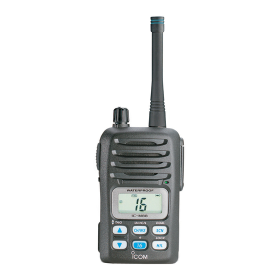
- Page 1 VHF MARINE TRANSCEIVER iC-m88...
- Page 2 INTRODUCTION This service manual describes the latest service information for the IC-M88 VHF MARINE TRANSCEIVER at the time of publication. Model Version Symbol AC adapter Power U.S.A. BC-147A IC-M88 S.E. Asia BC-147E To upgrade quality, all electrical or mechanical parts and inter- nal circuits are subject to change without notice or obligation.
-
Page 3: Table Of Contents
TABLE OF CONTENTS SECTION 1 SPECIFICATIONS SECTION 2 INSIDE VIEWS SECTION 3 DISASSEMBLY INSTRUCTIONS SECTION 4 CIRCUIT DESCRIPTION 4 - 1 RECEIVER CIRCUITS ....................4 - 1 4 - 2 TRANSMITTER CIRCUITS .................... 4 - 2 4 - 3 PLL CIRCUITS ........................ 4 - 3 4 - 4 POWER SUPPLY CIRCUITS .................. - Page 4 SECTION 1 SPECIFICATIONS ‘ ‘ GENERAL • Frequency coverage : TX: 156.050 MHz–157.425 MHz, RX: 156.050 MHz–163.275 MHz [MARINE] TX/RX: 146.000 MHz–174.000 MHz [LMR] • Number of free channels : 22 channels • Type of emission : 16K0G3E (Wide; 25 kHz) [MARINE] 16K0F3E (Wide;...
- Page 5 ‘ ‘ VHF MARINE CHANNEL LIST Channel No. Frequency (MHz) Channel No. Frequency (MHz) Channel No. Frequency (MHz) Transmit Receive Transmit Receive Transmit Receive 156.050 160.650 157.050 157.050 156.675 156.675 156.050 156.050 157.100 161.700 156.725 156.725 156.100 160.700 157.100 157.100 156.875 156.875 156.150...
- Page 6 SECTION 2 INSIDE VIEWS • LOGIC UNIT Bottom view *: Located under side of this point. AF mute circuit Q441* : 2SC4116 Q442* : CPH3403 Q443 : CPH3403 IN/EXT microphone switch Q444 : DTC144EU (Q461, Q462: UN911H) EEPROM Microphone amplifier (IC591*: HN58X2416TI) (IC471: NJM2904V) AF mute...
- Page 7 SECTION 3 DISASSEMBLY INSTRUCTIONS 1. Removing the chassis panel q Remove a nut (2 × 8 mm, black) and 3 screws w Unscrew 2 screws (2 × 4 mm, black) from the chassis. e Take off the chassis in the direction of the arrow. NOTE: * Tighten the screws in order of a number (q–y) when assembling.
-
Page 8: Circuit Description
SECTION 4 CIRCUIT DESCRIPTION 4-1 RECEIVER CIRCUITS The 1st IF signal is applied to a 2nd mixer section of the FM IF IC (IC231, pin 16). The signal is then mixed with a 2nd LO 4-1-1 ANTENNA SWITCHING CIRCUIT signal for conversion into a 450 kHz 2nd IF signal. (MAIN UNIT) The antenna switching circuit functions as a low-pass filter IC231 contains the 2nd mixer, limiter amplifier, quadrature... -
Page 9: Transmitter Circuits
4-1-5 SQUELCH CIRCUIT 4-2-2 MODULATION CIRCUIT (MAIN UNIT) (MAIN AND LOGIC UNITS) The modulation circuit modulates the VCO oscillating signal (RF signal) using the microphone audio signals. The noise squelch circuit cuts out AF signals when no RF signals are received. By detecting noise components in the The audio signals “MOCON”... -
Page 10: Pll Circuits
4-4 POWER SUPPLY CIRCUITS 4-3 PLL CIRCUIT (MAIN UNIT) VOLTAGE LINES 4-3-1 GENERAL The PLL circuit provides stable oscillation of the transmit fre- LINE DESCRIPTION quency and receive 1st LO frequency. The PLL output com- The voltage from the attached battery pack. pares the phase of the divided VCO frequency to the refer- The same voltage as the HV line (battery volt- ence frequency. - Page 11 4-5 PORT ALLOCATIONS 4-5-1 CPU (LOGIC UNIT; IC661) Port Port Description Description number name number name BEEP Outputs beep audio signals. Outputs scrambler mute signal for the STXMS AF mute circuit (IC481, pin 3). Outputs strobe signals for the scram- VSSTB Low : While scrambler is muting.
- Page 12 CPU–Continued 4-5-2 EXPANDER IC (MAIN UNIT; IC341) Port Port Description Description number name number name Input port for the [DOWN] key. Outputs the AF mute switch (IC281, DOWN pin 3) control signal. Low : While [DOWN] key is pushed. SRXMS Low : While the scrambler decord- Input port for the [CH/WX] key.
-
Page 13: Adjustment Procedures
: 10 MΩ/DC or better I SYSTEM REQUIREMENTS I STARTING SOFTWARE ADJUSTMENT q Connect IC-M88 and PC with the optional OPC-966 and • IBM PC compatible computer with an RS -232C serial port (38400 bps or faster) the RS-232C cable. - Page 14 • CONNECTION Standard signal generator to the antenna connector 0.1 V to 32 mV ( 127 dBm to 17 dBm) Attenuator deviation meter 40 dB or 50 dB CAUTION: DO NOT transmit while RF power meter SSG is connected to the 0.1 10 W/50 antenna connector.
- Page 15 • SCREEN DISPLAY EXAMPLE CS-M88 ADJ Rev.1.0 File Option COM 1: OPEN Connect Reload (F5) Disp para [A / D] [D / A] BATT : 120 : 78h : 7.53 V FRQCON : 127 : 7Fh : 2.49 V NOIS 59 : 3Bh : 1.16 V T1/POW : 92 : 5Ch :...
-
Page 16: Software Adjustment
5-2 SOFTWARE ADJUSTMENT Select an operation using [↑] / [↓] keys, then set specified value using [←] / [→] keys on the connected computer keyboard. MEASUREMENT ADJUSTMENT ADJUSTMENT CONDITION VALUE UNIT LOCATION PLL LOCK • Operating channel : center frequency MAIN Connect the 1.5–3.0 V (Verify) - Page 17 • MAIN UNIT TOP VIEW PLL lock voltage check point 5 - 5...
- Page 18 SOFTWARE ADJUSTMENT – continued • Select an operation using [↑] / [↓] keys, then set specified value using [←] / [→] keys on the connected computer keyboard. • “SQUELCH LEVEL ADJUSTMENT” must be performed after “RX SENSITIVITY ADJUSTMENT” is finished. •...
-
Page 19: Parts List
SECTION 6 PARTS LIST [VR UNIT] [LOGIC UNIT] ORDER ORDER DESCRIPTION DESCRIPTION R801 7210003130 VARIABLE TP76N97N-13F-10KA-2497 L421 6200010230 S.COIL EXCCL3216U1 C802 4030006860 S.CERAMIC C1608 JB 1H 102K-T R411 7030003560 S.RESISTOR ERJ3GEYJ 103 V (10 kΩ) R412 7030003560 S.RESISTOR ERJ3GEYJ 103 V (10 kΩ) R413 7030003620 S.RESISTOR ERJ3GEYJ 333 V (33 kΩ) - Page 20 [LOGIC UNIT] [LOGIC UNIT] ORDER ORDER DESCRIPTION DESCRIPTION R582 7030003440 S.RESISTOR ERJ3GEYJ 102 V (1 kΩ) C582 4030007090 S.CERAMIC C1608 CH 1H 470J-T R583 7410000750 S.ARRAY EXB-V4V 104JV (100 kΩ) C591 4030006900 S.CERAMIC C1608 JB 1H 103K-T R591 7030003560 S.RESISTOR ERJ3GEYJ 103 V (10 kΩ) C601 4030007050 S.CERAMIC...
-
Page 21: Main Unit
[MAIN UNIT] [MAIN UNIT] ORDER ORDER DESCRIPTION DESCRIPTION 1140005990 S.IC MB15A02PFV1-G-BND-ER 6200005540 S.COIL ELJNC R47K-F IC141 1110002750 S.IC TA75S01F (TE85R) 6200009460 S.COIL 0.25-1.9-7TL 67N IC231 1110003200 S.IC TA31136FN (EL) 6200005540 S.COIL ELJNC R47K-F IC251 1190000350 S.IC M62363FP-650C 6200008390 S.COIL 0.25-1.9-9TL IC261 1110003800 S.IC NJM2904V-TE1... - Page 22 [MAIN UNIT] [MAIN UNIT] ORDER ORDER DESCRIPTION DESCRIPTION ERJ3GEYJ 221 V (220 Ω) 7030003360 S.RESISTOR R244 7030003480 S.RESISTOR ERJ3GEYJ 222 V (2.2 kΩ) ERJ3GEYJ 331 V (330 Ω) 7030003380 S.RESISTOR R245 7030003640 S.RESISTOR ERJ3GEYJ 473 V (47 kΩ) ERJ3GEYJ 391 V (390 Ω) 7030003390 S.RESISTOR R246 7030003640 S.RESISTOR...
- Page 23 [MAIN UNIT] [MAIN UNIT] ORDER ORDER DESCRIPTION DESCRIPTION 4030007000 S.CERAMIC C1608 CH 1H 090D-T C160 4030009510 S.CERAMIC C1608 CH 1H 010B-T 4030007080 S.CERAMIC C1608 CH 1H 390J-T C161 4030007100 S.CERAMIC C1608 CH 1H 560J-T 4030006860 S.CERAMIC C1608 JB 1H 102K-T C162 4030006860 S.CERAMIC C1608 JB 1H 102K-T...
- Page 24 [MAIN UNIT] ORDER DESCRIPTION C314 4030009490 S.CERAMIC C1608 JB 1H 821K-T C315 4030011600 S.CERAMIC C1608 JB 1E 104K-T C316 4030008920 S.CERAMIC C1608 JB 1H 473K-T C322 4030006900 S.CERAMIC C1608 JB 1H 103K-T C323 4030006900 S.CERAMIC C1608 JB 1H 103K-T C324 4030006900 S.CERAMIC C1608 JB 1H 103K-T C325...
- Page 25 SECTION 7 MECHANICAL PARTS AND DISASSEMBLY [CHASSIS PARTS] [MAIN UNIT] ORDER ORDER QTY. QTY. DESCRIPTION DESCRIPTION MP41 8510013000 2336 VCO case Y534 6910014700 2600 ANT connector MP42 8510011101 1922 VCO cover-1 Y340A 7120000470 Jumper ERDS2T0 MP43 8930059890 Shield tape (M) 7120000470 Jumper ERDS2T0 MP111 8410002370...
- Page 26 NOTE 1 NOTE 2 MP45 (C) SP1 (C) J41 (C) MP44 (C) NOTE 1 MP32 (C) NOTE MP33 (C) NOTE 3 MP42 MP4 (C) MP31 (C) R801 (VR) MP43 NOTE3 MP66 (C) VR UNIT MP6 (C) MP46 (C) MP54 (C) MP65 (C) DS681 (L) MP682 (L) EP681 (L)
- Page 27 • BC-152 CHARGER PARTS LIST ELECTRICAL PARTS ACCESSORY PARTS ORDER ORDER ORDER QTY. QTY. DESCRIPTION QTY. DESCRIPTION DESCRIPTION 1180000970 S.IC AN78L05M-(E1) 7030000010 S.JUMPER MCR10EZHJ JPW (000) 8810001470 Screw.5 x 30 SUS 1190001180 S.IC MM1332BFBE 7030000010 S.JUMPER MCR10EZHJ JPW (000) 1110005960 S.IC S-80833CNMC-B8S-T2 7030000010...
- Page 28 SECTION SECTION 8 PARTS LIST SEMI-CONDUCTOR INFORMATION 8 - 1 TRANSISTORS AND FETS 8 - 2 DIODES • MAIN unit and LOGIC unit • MAIN unit and LOGIC unit 2SC4215 O/Y 2SA1588-GR 2SB1132 T100 Q 2SC4116 BL/GR 2SC4213-B 1SS375-TL 1SV245 1SV307 (TPH3) DAN222TL HVC350BTRF...
- Page 29 SECTION 9 BOARD LAYOUTS 9 - 1 CHARGER UNIT (BC-152) • TOP VIEW • BOTTOM VIEW 9-2 VR UNIT 9-3 CONNECTOR UNIT • TOP VIEW • BOTTOM VIEW • TOP VIEW • BOTTOM VIEW to LOGIC UNIT J411 J851 to MAIN UNIT J281 W802 R801...
- Page 30 9-2 MAIN UNIT • TOP VIEW The combination of this page and the next page shows the unit layout in the same configuration as the actual P.C. Board. LOGIC UNIT J401 VOLIN to VR unit BTYPE W802 V5VS R5VS T5VS MICO SMICO W/NS...
- Page 31 MAIN UNIT The combination of this page and the previous page • BOTTOM VIEW shows the unit layout in the same configuration as the actual P.C. Board. 9 - 3...
- Page 32 9-3 LOGIC UNIT The combination of this page and the next page shows the unit layout in the same configuration as the actual • TOP VIEW P.C. Board. 9 - 4...
-
Page 33: Logic Unit
LOGIC UNIT The combination of this page and the previous page shows the unit layout in the same configuration as the • BOTTOM VIEW actual P.C. Board. CP442 VOLIN BTYPE V5VS CP441 R5VS T5VS AFOUT MICO SMICO W/NS TEMPV LOINV J411 CDECV MAIN... -
Page 34: Block Diagram
SECTION 10 BLOCK DIAGRAM Q47: XP6501 RIPPLE MAIN UNIT ANTENNA LVINV D91: MA77 Q91: Q101: Q111: Q41: 2SC4226 D92: MA77 2SC5110 RD01MUS1 RD07MVS1 Q1: 2SK1829 Q3: 2SK880 Q61: 2SC4215 Q62: 2SC4215 D31-34: HVC350B TX/RX BUFF BUFF BUFF BUFF BUFF DRIVE 146 –174 MHz VCOS D39:... - Page 35 SECTION 11 VOLTAGE DIAGRAM Q47 XP6501 0.47µH V5FV V5FV PLL5V 150k LOCK: 4.85V 470p 4.78V UNLK: 0.50V VR UNIT 0.001 J281 VCO CASE R3 1k W802 MA2S111 2.2k UNLKI UNLKI IC1 MB15A02PFV-1 SCLK 0.47µH W802 HVC350B HVC350B PLLIN SDATA CLOCK DATA PLSTB PLSTB...
- Page 36 R122 VCO CASE EP111 V5FV 0.001 TX: 3.51V TX: 4.86V C128 C129 1.5k 2SC4226 RX: 3.42V RX: 0.0V L124 470p 0.01 TX: 3.52V EP101 0.001 2.7µH D131 C131 L131 L132 C106 RX: 3.46V 80nH C114 C115 L112 1SV307 0.001 30nH 32nH 0.75p 0.001...
- Page 37 LEDS1 LEDS1 LEDS2 LEDS2 DS681 CONT2 L2-0390TAY LOGIC UNIT W/NS W/NS CONT1 J401 DS651 DS653 VOLIN VOLIN FY1101F-TR SML-311YT C642 C641 LED ON: 5.00V 0.01 BTYPE BTYPE DS652 DS654 SEG9 VSS0 FY1101F-TR SML-311YT CPU5V SEG8 VDD0 S641 SEG7 CONT2 EVQ-PUL SEG6 R651 R652...
- Page 39 S-13909MZ-C2 1-1-32, Kamiminami, Hirano-ku, Osaka 547-0003, Japan © 2002 Icom Inc.
Need help?
Do you have a question about the IC-M88 and is the answer not in the manual?
Questions and answers