Samsung HT-BD1255 Service Manual
5.1ch blu-ray home theater system
Hide thumbs
Also See for HT-BD1255:
- User manual (104 pages) ,
- User manual (101 pages) ,
- User manual (93 pages)
Table of Contents
Advertisement
Quick Links
SERVICE
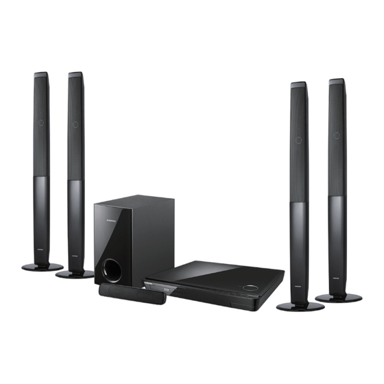
5.1CH Blu-ray Home Theater System
HT-BD1255
Refer to the service manual in the GSPN (see the rear cover) for the more information.
5.1CH Blu-ray
Home Theater System
Model Name : HT-BD1255
Model Code : HT-BD1255T/XAC
Speaker
PS-BD1255
Front
PS-FBD1255
Center
PS-CBD1255
Rear
PS-RBD1255
Subwoofer
PS-WBD1255
Manual
1. Precaution
2. Product Specification
3. Disassembly & Reassembly
4. Troubleshooting
5. Exploded View & Part List
6. PCB Diagram
7. Schematic Diagram
CONTENTS
Advertisement
Chapters
Table of Contents

Related Manuals for Samsung HT-BD1255


Summary of Contents for Samsung HT-BD1255
- Page 1 5.1CH Blu-ray Home Theater System Model Name : HT-BD1255 Model Code : HT-BD1255T/XAC Speaker PS-BD1255 Front PS-FBD1255 Center PS-CBD1255 Rear PS-RBD1255 Subwoofer PS-WBD1255 SERVICE Manual 5.1CH Blu-ray Home Theater System CONTENTS 1. Precaution 2. Product Specification 3. Disassembly & Reassembly 4.
- Page 2 Asia asia.samsungportal.com Mideast & Africa mea.samsungportal.com © Samsung Electronics Co.,Ltd. Apr. 2009 This Service Manual is a property of Samsung Electronics Printed in Korea Co.,Ltd. Any unauthorized use of Manual can be punished under applicable International and/or domestic law.
-
Page 3: Table Of Contents
Contents 1. Precaution 1-1 Safety Precautions ................... 1-1 1-2 Servicing Precautions ..................1-3 1-3 Precautions for Electrostatically Sensitive Devices (ESDs) ......1-4 2. Product Specification 2-1 Product Feature ....................2-1 2-2 Specifications ....................2-2 2-3 Specifications Analysis ..................2-8 2-4 Accessories ......................2-10 3. Disassembly & Reassembly 3-1 Overall Disassembly &... - Page 4 Contents 6. PCB Diagram 6-1 Wiring Diagram ....................6-2 6-2 FRONT PCB Top ....................6-3 6-3 FRONT PCB Bottom ..................6-5 6-4 KEY PCB Top ....................6-6 6-5 KEY PCB Bottom ..................... 6-8 6-6 AMP PCB Top ....................6-9 6-7 AMP PCB Bottom ..................... 6-11 6-8 MAIN PCB Top ....................
-
Page 5: Precaution
1 and 5.2 megohms. If there is no return path, the measured resistance should be “infinite.” If the resistance is outside these limits, a shock hazard might exist. See Fig. 1-2 Samsung Electronics... - Page 6 . Use replacement components that have the same ratings, especially for flame resistance and dielectric strength specifications. A replacement part that does not have the same safety characteristics as the original might create shock, fire or other hazards. Samsung Electronics...
-
Page 7: Servicing Precautions
8. Always connect a test instrument’s ground lead to the instrument chassis ground before connecting the positive lead; always remove the instrument’s ground lead last. First read the “Safety Precautions” section of this manual. If some unforeseen circumstance creates a conflict between the servicing and safety precautions, always follow the safety precautions. Samsung Electronics... -
Page 8: Precautions For Electrostatically Sensitive Devices (Esds)
9. Minimize body motions when handing unpackaged replacement ESDs. Motions such as brushing clothes together, or lifting a foot from a carpeted floor can generate enough static electricity to damage an ESD. Samsung Electronics... -
Page 9: Product Specification
• Progressive Mode • Still Mode • BD Wise • Picture Control HT-BD2 → HT-BD1250 - DivX (Only EU) - PC Connected - USB HOST - Profile 2.0 Ready - Netflix, Pandora - I-POD Docking (Only USA) - Wireless Rear Speaker Samsung Electronics... -
Page 10: Specifications
Product Specification 2-2 Specifications 2-2-1 HT-BD1250 / HT-BD1252 / HT-BD1255 Specifications Basic Specification Power Consumption 85 W Weight 4.4 Kg GENERAL Dimensions 440 (W) x 345 (D) x 63 (H) mm Operating Temperature Range +5°C ~ +35°C Operating Humidity Range 10% to 75% BD (Blu-ray Disc) Reading Speed: 4.917m/sec Reading Speed: 3.49 ~ 4.06 m/sec. - Page 11 Surround : 100 x 151 x 89 mm Dimensions (W x H x D) Centre : 300 x 59 x 50 mm Subwoofer : 201 x 403 x 410 mm Front: 2.18 Kg, Surround: 0.42 Kg Weights Centre: 0.32 Kg, Subwoofer: 5.39 Kg Samsung Electronics...
- Page 12 Product Specification HT-BD1255 Speaker Specification 5.1ch Speaker System Speaker system Front Surround Center Subwoofer Impedance 3Ω 3Ω 3Ω 3Ω 140Hz ~ 140Hz ~ 140Hz ~ 40Hz ~ Frequency range 50KHz 20KHz 20KHz 160Hz Output sound pressure level 87dB/W/M 87dB/W/M 87dB/W/M 88dB/W/M SPEAKER Rated input 165W 165W 170W...
- Page 13 PCM multi channel audio, Bit stream audio, PCM audio Front speaker output 165W x 2 (3Ω) Center speaker output 170W (3Ω) Analog input: 20Hz ~ 20kHz (±3dB) Frequency range AMPLIFIER Digital input: 20Hz ~ 44kHz (±3dB) S/N Ratio 70dB Channel separation 60dB Input sensitivity (AUX) 500mV Samsung Electronics...
- Page 14 140Hz ~ 50KHz 40Hz ~ 160Hz Output sound pressure level 87dB/W/M 90dB/W/M SPEAKER Rated input 165W 170W Maximum input 330W 340W Front: 100.5 x 210 x 99 mm Dimensions (W x H x D) Subwoofer: 201 x 403 x 410 mm Front: 0.70 Kg Weights Subwoofer: 5.39 Kg Samsung Electronics...
- Page 15 DVD playback Component Component Output HDMI Output [HDMI [HDMI not CVBS Output Remark Setup Connected] Connected] 1080P@60F 1080P@60F 480i 480P 480i 1080i 1080i 480i 480P 480i 720P 720P 480i 480P 480i 480P 480P 480i 480P 480i 480i 480P 480i 480i 480i Samsung Electronics...
-
Page 16: Specifications Analysis
(Progressive Mode, Still Mode, BD Wise, Picture Control) Video Processor Main SOC Internal Scaler Main SOC Internal Scaler 1080p 60frame 1080i 60frame 1080p 24frame Video 480i/p video output for Blu-ray Simultaneous Video Output between HDMI/ Component/CVBS : application, X: non-application Samsung Electronics... - Page 17 HD audio bit stream dts-HD HRA dts-HD HRA output on HDMI 1.3 TrueHD TrueHD SMPS 2 trans 2 trans Deck Draw type Plastic Cover Slot-In Pick Up 5G VE Pickup 4G VE Pickup Front Micom SANYO SANYO Main ↔ Loader One Board P-ATA : application, X: non-application Samsung Electronics...
-
Page 18: Accessories
Product Specification 2-4 Accessories 2-4-1 Supplied Accessories Accessories Item Item code Remark Remote Control AH59-02144K Battery 4301-000116 HDMI Cable AH39-00923A Audio Cable AH39-40001V Samsung Service Center FM Antenna AH42-00021A AH68-02178S User’s Manual AH68-02183M Cloth Clean AH81-02286C 2-10 Samsung Electronics... -
Page 19: Disassembly & Reassembly
Be careful not to make any scratches as you remove it. DECO-TOP 1) Unfasten 3 screws on the DECO- TOP. : BH,+,-,B,M3,L10,ZPC(BLK) 2) Move DECO-TOP a little on the direction of Rear. 3) Disconnect FPC wire and remove DECO-TOP. Samsung Electronics... - Page 20 2) Loosen hooks from CABINET- BOTTOM. 3) Remove CABINET-FRONT from CABINET-BOTTOM. BRACKET- 1) Unfasten 8 screws on the BRACKET- TOP. : BH,+,-,B,M3,L10,ZPC(BLK) 2) Remove BRACKET-TOP from CABINET-BOTTOM. DECK 1) Unfasten 4 screws and remove DECK from CABINET-BOTTOM. : BH,+,-,B,M3,L10,ZPC(BLK) Samsung Electronics...
- Page 21 BOTTOM. SMPS PCB 1) Unfasten 5 screws on the SMPS PCB. : BH,+,-,B,M3,L10,ZPC(BLK) 2) Remove SMPS PCB from CABINET- BOTTOM. FRONT PCB 1) Unfasten 2 screws on the FRONT PCB. : BH,+,-,B,M3,L10,ZPC(BLK) 2) Remove FRONT PCB from CABINET-BOTTOM. Samsung Electronics...
-
Page 22: Deck Disassembly & Reassembly
Disassembly & Reassembly 3-2 DECK Disassembly & Reassembly Part Name Description Ass'y Cover 1) Remove 4 Screws 1. 2) Lift up the Ass’y Cover 2 in direction of arrow. 4 SCREWS (2X7 W) ASS'Y COVER Samsung Electronics... - Page 23 3) Pull the Tray Disc 3 to disassemble, while simultaneously pushing 2 Stoppers 4 (left, right) in the direction arrow “B”, “C”. SCREW DRIVER TRAY GEAR HOLE OPEN CLOSE TRAY DISC (BOTTOM VIEW) STOPPER “B” “A” “C” TRAY DISC (TOP VIEW) Samsung Electronics...
- Page 24 1) Remove FFC Cable 1, 2, 3. Deck 2) Remove 4 Screws 4 from the Ass’y P/U Deck 5 and lift it up. FFC CABLE FFC CABLE (BOTTOM VIEW) 4 SCREWS (2.6X6 W) FFC CABLE ASS'Y P/U DECK (TOP VIEW) Samsung Electronics...
- Page 25 3) Lift Up Shaft P/U 4 and Remove the Ass’y Pick Up 5. 1 SCREW (1.7X5 W) ASS'Y HINGE PU BRACKET SHAFT PU “A” “A” (BOTTOM VIEW) ASS'Y PICK UP BRACKET SHAFT PU SHAFT P/U BRACKET SHAFT PU (TOP VIEW) Samsung Electronics...
- Page 26 3) Insert the Ass’y Hinge PU 6 Assemble 1 Screw 5. SHAFT P/U ASS'Y PICK UP SHAFT P/U ASS'Y PICK UP SHAFT P/U ASS'Y PICK UP BRACKET SHAFT PU BRACKET SHAFT PU SHAFT P/U SHAFT P/U (OK) (NG) BRACKET SHAFT PU 1 SCREW (1.7X5 W) ASS'Y HINGE PU Samsung Electronics...
-
Page 27: Troubleshooting
Troubleshooting 4. Troubleshooting Checkpoints by Error Mode ..............4-2 Initialization & Upgrade Methods............4-34 Buyer-Region Code Setting Method ...........4-38 Samsung Electronics... -
Page 28: Checkpoints By Error Mode
FL1 (250V/10A) is normal? Test SMPS PCB Change BDL1 BDL1 (TPS10P05G) is normal? Test SMPS PCB Change IC2 IC2 (ICE3B0365J) is normal? Test SMPS PCB Change PCA3 PCA3 (PC817) is normal? Test SMPS PCB Change the SMPS PCB Samsung Electronics... - Page 29 Troubleshooting 4-1-2 AMP NO POWER AMP No Power (Stand by LED ON) Change IC1 IC1 (MR4040) is normal? Test SMPS PCB Change PCA3 PCA1, 2 (PC817) is normal? Test SMPS PCB Change the SMPS PCB Samsung Electronics...
- Page 30 Refer to image of Fig. 4-1. Check AL01~06 of AMP PCB? Change AMP PCB ; Output Check Refer to image of Fig. 4-2-1 and Fig. 4-2-2. Check the signal from jack and if not, change AMP PCB. Samsung Electronics...
- Page 31 Troubleshooting AMP, page 7-5 1 N O C AMP PCB Top, page 6-9 <Fig. 4-1> Samsung Electronics...
- Page 32 Troubleshooting AMP, page 7-5 <Fig. 4-2-1> Samsung Electronics...
- Page 33 Troubleshooting AIC5 AIC6 AIC3 AIC4 AIC1 AIC2 UPIC1 AIC11 AMP PCB Top, page 6-9 <Fig. 4-2-2> Samsung Electronics...
- Page 34 OP AMP IC OUTPUT CHECK AIC7, 8, 9 (4560) AIC7, 8, 9 (4560) POWER (+5V, -5V) Pin 1, 7 Check Pin 8, 4 Check Refer to wave pattern image of Fig. 4-4-1 Replace AIC7, 8, 9. and Fig. 4-4-2. A Samsung Electronics...
- Page 35 AIC1, 2, 3, 4, 5, 6 (IRS2092S) 5, 6 (IRS2092S) POWER (+5V, -5V) Pin 11, 14 Check Pin 1, 6 Check Refer to wave pattern image of Fig. 4-5-1 Replace AIC1, 2, 3, 4, 5, 6. and Fig. 4-5-2. SOUND OUTPUT OK Samsung Electronics...
- Page 36 Troubleshooting AMP, page 7-5 UPIC1 AMP PCB Top, page 6-9 <Fig. 4-3> 4-10 Samsung Electronics...
- Page 37 Troubleshooting AMP, page 7-5 <Fig. 4-4-1> Samsung Electronics 4-11...
- Page 38 Troubleshooting 9 8 7 C C C I I I A A A AMP PCB Bottom, page 6-11 <Fig. 4-4-2> 4-12 Samsung Electronics...
- Page 39 Troubleshooting AMP, page 7-5 <Fig. 4-5-1> Samsung Electronics 4-13...
- Page 40 Troubleshooting AIC5 AIC6 AIC3 AIC4 AIC1 AIC2 UPIC1 AIC11 AMP PCB Top, page 6-9 <Fig. 4-5-2> 4-14 Samsung Electronics...
- Page 41 Disc Ioading error Check the FEU1, IC23 → 8V, 5V Check the Power PiC1 → 3.3V PICKUP cable and Reinsert cables again Motor cable inserted correctly? Change the MAIN PCB Check the clock at X1 25MHz Change the DECK Samsung Electronics 4-15...
- Page 42 (between Front panel & Main) OK? Check REYE or change the REYE Pin 1 Signal OK? FRONT PCB Refer to wave pattern image of Fig. 4-6. Change MAIN PCB FMIC1 Pin 47 or change the MAIN PCB 4-16 Samsung Electronics...
- Page 43 Troubleshooting <Remote Eye Data> FRONT, page 7-3 TCON1 FRONT PCB Top, page 6-3 <Fig. 4-6> Samsung Electronics 4-17...
- Page 44 Troubleshooting 4-1-7 NO PICTURE No Picture Logo screen is OK? HDMI? NO LOGO HDMI BD/DVD Playback is OK? Component? NO LOGO COMPONENT Change the MAIN PCB NO LOGO CVBS 4-18 Samsung Electronics...
- Page 45 (2V ~ 5V) Data output from IC18? Check IC18 power input and (Pin 30, 31, 33, 34, 36, 37, peripheral devices 39, 40) Refer to wave pattern image of Fig. 4-9. HDMI Cable Error Samsung Electronics 4-19...
- Page 46 Troubleshooting <Digital Video Signal> HDMI CEC / TX (SIL9134), page 7-7 1 C I E C IC18 MAIN PCB Top, page 6-13 <Fig. 4-7> 4-20 Samsung Electronics...
- Page 47 Troubleshooting <54MHz Crystal> CLOCK, BBS, page 7-10 1 C I E C MAIN PCB Top, page 6-13 <Fig. 4-8> Samsung Electronics 4-21...
- Page 48 Troubleshooting <HDMI OUTPUT DATA> HDMI CEC / TX (SIL9134), page 7-7 1 C I E C IC18 MAIN PCB Top, page 6-13 <Fig. 4-9> 4-22 Samsung Electronics...
- Page 49 Refer to wave pattern image of Fig. 4-10. Check VIC1 soldering of peripheral Video output from devices VIC1 & VC6, VC1, VC4 Refer to wave pattern image of Fig. 4-11. Component Cable Error Samsung Electronics 4-23...
- Page 50 AUDIO / VIDEO (COMPONENT, COMPOSITE), page 7-6 8 1 N O C 1 C I E C IC18 MAIN PCB Top, page 6-13 VR12 VR13 VR14 <VR12 Y Signal> <VR13 Pb Signal> <VR14 Pr Signal> <Fig. 4-10> 4-24 Samsung Electronics...
- Page 51 Troubleshooting AUDIO / VIDEO (COMPONENT, COMPOSITE), page 7-6 AIC3 VIC1 MAIN PCB Bottom, page 6-10 <VC6 Y Signal> <VC1 Pb Signal> <VC4 Pr Signal> <Fig. 4-11> Samsung Electronics 4-25...
- Page 52 VCN1 (VR16) soldering error VCN1 (VR16) Refer to wave pattern image of Fig. 4-12. Check VIC1 soldering of peripheral Video output from devices VIC1 & VC3 Refer to wave pattern image of Fig. 4-13. Component Cable Error 4-26 Samsung Electronics...
- Page 53 Troubleshooting AUDIO / VIDEO (COMPONENT, COMPOSITE), page 7-6 VR16 8 1 N O C <Composit Output CVBS Color Bar VR16> PIC6 DIC1 MAIN PCB Top, page 6-13 <Fig. 4-12> Samsung Electronics 4-27...
- Page 54 Troubleshooting AUDIO / VIDEO (COMPONENT, COMPOSITE), page 7-6 AIC3 VIC1 <Composit CVBS Color Bar VC3> MAIN PCB Top, page 6-13 <Fig. 4-13> 4-28 Samsung Electronics...
- Page 55 Only DVD NG? RFIP Check? Signal level OK? BD: over 400mV DVD: over 200mV CD: over 200mV Refer to image of Only CD NG? Fig. 4-16. Change the MAIN PCB Change the MAIN PCB Change the DECK Samsung Electronics 4-29...
- Page 56 Troubleshooting BCM7620 (F/E), page 7-20 6 1 N O C 3 1 C I E F CON15 MAIN PCB Top, page 6-13 <Fig. 4-14> 4-30 Samsung Electronics...
- Page 57 Troubleshooting BCM7620 (F/E), page 7-20 DBGN1 DSCN1 DSIC14 CON17 CON15 MAIN PCB Top, page 6-13 MAIN PCB Bottom, page 6-16 <Fig. 4-15> Samsung Electronics 4-31...
- Page 58 Troubleshooting BCM7620 (F/E), page 7-20 FEIC13 CON15 MAIN PCB Bottom, page 6-16 <Fig. 4-16> 4-32 Samsung Electronics...
- Page 59 The connection between LAN and SET is direct. So there is no need to check H/W if there is network problem. If it is, the problem is MAIN CHIP(U1)'s BGA soldering problem. It must be changed to new board. Samsung Electronics 4-33...
-
Page 60: Initialization & Upgrade Methods
- LDR: Loader F/W (Updatable) - Front: Front Micom F/W (Not Updatable, and don’t need to mostly) - Software: Blu-ray Disc, DVD, CD, Main (Updatable) - Region: BD region code / DVD region code - Macrovision 4-34 Samsung Electronics... - Page 61 (If the update CD you inserted is a later one than Yes Current Version) 4. Get rid of update CD from the Disc Tray. Firmware Update. Now, Processing... 5. Wait about 2~3 minutes. Please, do not turn off the power. 6. When Finished, power automatically goes off. Samsung Electronics 4-35...
- Page 62 Troubleshooting F/W Update via Network 4-36 Samsung Electronics...
- Page 63 3. Then, VFD sign: ‘COLD START’ Macrovision : BBS41 4. System Micom Cold Start : During Stand-By, just press on the front panel for over 5 seconds. Then, Red LED will go out and go on. Samsung Electronics 4-37...
-
Page 64: Buyer-Region Code Setting Method
Please remind that “T-MODE” indicator on the VFD is appeared for a very short time. 4. After step (3), you can see “TEST − −” on the VFD. Insert number “3”, “3” to select Region Code. TEST − − 4-38 Samsung Electronics... - Page 65 Australia Only models which supporting semi-karaoke Russia (semi_mic) not including midi file. Russia (full_mic) Full karaoke models which support midi file. Africa China (semi_mic) Brazil Canada For example, insert 00 to select USA. 0 − Samsung Electronics 4-39...
- Page 66 In this case, you have to change System Micom, and set up the Buyer Region code again. In case of EEPROM, you don't need to care about it. After set-up the Region code, System Micom will store the information of the region code to EEPROM automatically. 4-40 Samsung Electronics...
-
Page 67: Exploded View & Part List
Exploded View & Part List 5. Exploded View & Part List 5-1 Product Exploded View ...............5-2 5-2 DECK Exploded View ................5-4 5-3 Speaker System..................5-6 5-4 Electrical Part List ................5-7 Samsung Electronics This Document can not be used without Samsung’s authorization. -
Page 68: Product Exploded View
Exploded View & Part List 5-1 Product Exploded View AA505 T0076 AC501 AK420 AL210 VOLCA AD330 AM020 AB501 AD150 T0076 AL180 AS260 T0076 AC010 FL261 AD340 VFILT AD502 AD504 S.N.A: Service Not Available This Document can not be used without Samsung’s authorization. Samsung Electronics... - Page 69 ASSY PCB FRONT;BD HOME THEATER,HT-BD1250 PCB-KEY AH92-03060A ASSY PCB KEY;BD HOME THEATER,HT-BD1250,H PCB-MAIN AH92-03052A ASSY PCB MAIN;BD HOME THEATER,HT-BD1250, PCB-SMPS AH44-00202A SMPS-HP;HD-BD1250,ORTP-527,150~200W,AC POWER CORD 3903-000402 CBF-POWER CORD;AT,US,EP2,HOUSING(2P),125 6003-001561 SCREW-TAPTYPE;BH,+,-,B,M3,L6,ZPC(WHT),SW 6003-000275 SCREW-TAPTYPE;BH,+,B,M3,L10,ZPC(BLK),SWR 6003-000282 SCREW-TAPTYPE;BH,+,-,B,M3,L8,ZPC(BLK),SW Samsung Electronics This Document can not be used without Samsung’s authorization.
-
Page 70: Deck Exploded View
( 2 x 7 W SCREW ) H200 H400 H401 ( 1.7 x 5 W SCREW ) PICK UP H301 W900 ( 2.6 x 6 W SCREW ) H300 H301 H100 H501 H500 This Document can not be used without Samsung’s authorization. Samsung Electronics... - Page 71 SCREW-TAPPING; PH,+,-,B,M1.7,L5.0,ZPC H500 AK92-01850A ASSY PCB-RELAY; BD-P5B,BD-P1250,-,- H501 AK41-00891A FFC-PU CABLE; BD-P1250,B TYPE,0.5 PIT PICKUP AK96-01004A ASSY PICK UP-BP5; SOH-BP5,BD-PLAYER,-,- W900 6003-001449 SCREW-TAPTITE; BH,+,B,M2.6,L6,NI PLT W901 6003-001199 SCREW-TAPTITE; PWH,+,-,B,M2,L7,ZPC(WH Samsung Electronics This Document can not be used without Samsung’s authorization.
-
Page 72: Speaker System
Rear Speaker SPEAKER-AH81-05111;PS-BD1250,CENTER AH81-05111B SPEAKER,SYSTEM,UHL,XXA,-,-,-,- Rear Speaker SPEAKER;PS-BD1250,REAR SPEAKER AH81-05112B SYSTEM,R,UHL XXA,-,-,-,- SPEAKER-SUBWOOFER;PS-BD1250,CENTER Subwoofer AH81-05127B SPEAKER,SYSTEM,UHL,XXA,-,-,-,- SPEAKER;PS-Q20,SPK CORD,CONNECTOR,FRONT/ Speaker Wire AH81-02177B SUB W/F:4M,CENTER:3M SPEAKER;STAND_F,100*100*17,ABS , Glossy,PART Stand AH81-04670A FOR PS-Z520,-,-,- This Document can not be used without Samsung’s authorization. Samsung Electronics... -
Page 73: Electrical Part List
2007-000066 R-CHIP;20Kohm,1%,1/10W,TP,1608 AH59-02203B SPEAKER SYSTEM;HT-BD1250,XXA 5.1CH, VCON2 3708-001618 CONNECTOR-FPC/FFC/PIC;5P,1mm,SMD-A, AH81-05121A CUSHION-SUBWOOFER;PS-BD1250,SUBWOOF 1 AH81-05127B SPEAKER-SUBWOOFER;PS-BD1250,SUBWOOF 1 VLED1 0601-001949 LED;SMD,BLUE,1.6x0.8x0.4mm,468nm,1 AH81-04675A SPEAKER;FRONT PANEL-SW,FOR PS-Z520, VLED2 0601-001949 LED;SMD,BLUE,1.6x0.8x0.4mm,468nm,1 AH81-04922A SPEAKER-A/S PART;CABINET SUBWOOFER, VLED3 0601-001949 LED;SMD,BLUE,1.6x0.8x0.4mm,468nm,1 VLED4 0601-001949 LED;SMD,BLUE,1.6x0.8x0.4mm,468nm,1 AH81-04971A A/S;SUBWOOFER UNIT,FOR PS-WZ520,16 Samsung Electronics This Document can not be used without Samsung’s authorization. - Page 74 2007-000458 R-CHIP;18Kohm,5%,1/10W,TP,1608 USC1 2203-005249 C-CER,CHIP;100nF,10%,50V,X7R,TP,160 ADR23 2007-000140 R-CHIP;1Kohm,5%,1/16W,TP,1005 USC5 2203-006361 C-CER,CHIP;10000nF,10%,10V,X5R,TP,2 ADR24 2007-000138 R-CHIP;100ohm,5%,1/16W,TP,1005 USD1 0406-001128 DIODE-TVS;MLVS-0603-E08,50V ADR25 2007-000138 R-CHIP;100ohm,5%,1/16W,TP,1005 VCON1 3708-001618 CONNECTOR-FPC/FFC/PIC;5P,1mm,SMD-A, VFC1 2203-006361 C-CER,CHIP;10000nF,10%,10V,X5R,TP,2 ADR26 2007-000138 R-CHIP;100ohm,5%,1/16W,TP,1005 This Document can not be used without Samsung’s authorization. Samsung Electronics...
- Page 75 2203-006361 C-CER,CHIP;10000nF,10%,10V,X5R,TP,2 C306 2203-006158 C-CER,CHIP;100nF,10%,16V,X7R,1005 C88 2203-006361 C-CER,CHIP;10000nF,10%,10V,X5R,TP,2 C31 2203-006158 C-CER,CHIP;100nF,10%,16V,X7R,1005 C311 2404-001035 C-TA,CHIP;10uF,10%,25V,-,TP,6032 C89 2203-006361 C-CER,CHIP;10000nF,10%,10V,X5R,TP,2 C313 2402-001237 C-AL,SMD;330uF,20%,6.3V,-,TP,6.3x7. C90 2203-006361 C-CER,CHIP;10000nF,10%,10V,X5R,TP,2 C314 2402-001276 C-AL,SMD;47uF,20%,35V,TP,6.6x6.6x5. C91 2203-006361 C-CER,CHIP;10000nF,10%,10V,X5R,TP,2 Samsung Electronics This Document can not be used without Samsung’s authorization.
- Page 76 3301-001069 BEAD-SMD;120ohm,1.6x0.8x0.8mm,200mA 0403-001203 DIODE-ZENER;5245B,14.25-15.75V,225m DPC23 2203-006158 C-CER,CHIP;100nF,10%,16V,X7R,1005 DC1 2203-001656 C-CER,CHIP;0.47nF,5%,50V,NP0,1608 DPC24 2203-006158 C-CER,CHIP;100nF,10%,16V,X7R,1005 DC10 2203-006158 C-CER,CHIP;100nF,10%,16V,X7R,1005 DPC25 2203-006158 C-CER,CHIP;100nF,10%,16V,X7R,1005 DPC26 2203-006158 C-CER,CHIP;100nF,10%,16V,X7R,1005 DC11 2203-006361 C-CER,CHIP;10000nF,10%,10V,X5R,TP,2 DPC27 2203-006158 C-CER,CHIP;100nF,10%,16V,X7R,1005 5-10 This Document can not be used without Samsung’s authorization. Samsung Electronics...
- Page 77 2007-001292 R-CHIP;33ohm,5%,1/16W,TP,1005 DR80 2007-000402 R-CHIP;150ohm,5%,1/10W,TP,1608 DPR34 2007-001292 R-CHIP;33ohm,5%,1/16W,TP,1005 DR81 2007-001292 R-CHIP;33ohm,5%,1/16W,TP,1005 DR85 2007-001292 R-CHIP;33ohm,5%,1/16W,TP,1005 DPR35 2007-001292 R-CHIP;33ohm,5%,1/16W,TP,1005 DR86 2007-001292 R-CHIP;33ohm,5%,1/16W,TP,1005 DPR36 2007-001292 R-CHIP;33ohm,5%,1/16W,TP,1005 DPR37 2007-000140 R-CHIP;1Kohm,5%,1/16W,TP,1005 DR90 2007-001292 R-CHIP;33ohm,5%,1/16W,TP,1005 Samsung Electronics This Document can not be used without Samsung’s authorization. 5-11...
- Page 78 2203-006048 C-CER,CHIP;100nF,10%,10V,X7R,1005 FEC100 2203-006048 C-CER,CHIP;100nF,10%,10V,X7R,1005 FEC34 2203-006158 C-CER,CHIP;100nF,10%,16V,X7R,1005 FEC101 2203-006048 C-CER,CHIP;100nF,10%,10V,X7R,1005 FEC102 2203-005249 C-CER,CHIP;100nF,10%,50V,X7R,TP,160 FEC373 2404-000284 C-TA,CHIP;10uF,20%,16V,-,TP,3528 FEC103 2203-006048 C-CER,CHIP;100nF,10%,10V,X7R,1005 FEC375 2203-006158 C-CER,CHIP;100nF,10%,16V,X7R,1005 FEC104 2203-006048 C-CER,CHIP;100nF,10%,10V,X7R,1005 FEC4 2203-006048 C-CER,CHIP;100nF,10%,10V,X7R,1005 5-12 This Document can not be used without Samsung’s authorization. Samsung Electronics...
- Page 79 2007-001292 R-CHIP;33ohm,5%,1/16W,TP,1005 FER121 2007-000170 R-CHIP;1Mohm,5%,1/16W,TP,1005 FER967 2007-000141 R-CHIP;2.2Kohm,5%,1/16W,TP,1005 FER18 2007-000157 R-CHIP;47Kohm,5%,1/16W,TP,1005 FER98 2007-000148 R-CHIP;10Kohm,5%,1/16W,TP,1005 FER19 2007-000157 R-CHIP;47Kohm,5%,1/16W,TP,1005 FER99 2007-001014 R-CHIP;51ohm,5%,1/10W,TP,1608 FEU1 1203-002253 IC-POSI.FIXED REG.;KIA7808AF,DPAK,3 FER2 2007-000138 R-CHIP;100ohm,5%,1/16W,TP,1005 FEU2 1003-002187 IC-MOTOR DRIVER;AM9268,SOP,42P,18x7 Samsung Electronics This Document can not be used without Samsung’s authorization. 5-13...
- Page 80 2203-006048 C-CER,CHIP;100nF,10%,10V,X7R,1005 IPL8 2901-001302 FILTER-EMI SMD;20V,0.3A,0pF,2.0x1.2 HC7 2203-006048 C-CER,CHIP;100nF,10%,10V,X7R,1005 IPVR1 2007-001164 R-CHIP;75ohm,1%,1/10W,TP,1608 IPVR2 2007-001164 R-CHIP;75ohm,1%,1/10W,TP,1608 HC8 2203-006048 C-CER,CHIP;100nF,10%,10V,X7R,1005 IPX1 2801-004021 CRYSTAL-SMD;24.576MHz,20ppm,28-AAN, HC9 2203-006048 C-CER,CHIP;100nF,10%,10V,X7R,1005 HCN1 3701-001313 CONNECTOR-HDMI;19P,2R,PLUG,ANGLE,AU L1112 3301-001655 BEAD-SMD;33ohm,3216,3000mA,TP,16ohm 5-14 This Document can not be used without Samsung’s authorization. Samsung Electronics...
- Page 81 MURN11 2011-001344 R-NETWORK;100ohm,5%,1/16W,L,CHIP,8P MEM3 1105-001942 IC-DDR2 SDRAM;K4T1G164Q,DDR2,1Gbit, MURN111 2011-001344 R-NETWORK;100ohm,5%,1/16W,L,CHIP,8P MEM4 1105-001942 IC-DDR2 SDRAM;K4T1G164Q,DDR2,1Gbit, MR10 2007-000043 R-CHIP;1Kohm,1%,1/10W,TP,1608 MURN12 2011-001344 R-NETWORK;100ohm,5%,1/16W,L,CHIP,8P MR4 2007-000779 R-CHIP;33ohm,1%,1/10W,TP,1608 MURN13 2011-001344 R-NETWORK;100ohm,5%,1/16W,L,CHIP,8P MR5 2007-000779 R-CHIP;33ohm,1%,1/10W,TP,1608 MURN14 2011-001344 R-NETWORK;100ohm,5%,1/16W,L,CHIP,8P Samsung Electronics This Document can not be used without Samsung’s authorization. 5-15...
- Page 82 2203-000438 C-CER,CHIP;1nF,10%,50V,X7R,1005 PC50 2203-006361 C-CER,CHIP;10000nF,10%,10V,X5R,TP,2 PR11 2007-000287 R-CHIP;100ohm,1%,1/10W,TP,1608 PC51 2203-006361 C-CER,CHIP;10000nF,10%,10V,X5R,TP,2 PR12 2007-008275 R-CHIP;30Kohm,1%,1/16W,TP,1005 PC52 2203-006361 C-CER,CHIP;10000nF,10%,10V,X5R,TP,2 PR13 2007-008426 R-CHIP;12.4Kohm,1%,1/10W,TP,1608 PR14 2007-000076 R-CHIP;330ohm,5%,1/10W,TP,1608 PC55 2203-006361 C-CER,CHIP;10000nF,10%,10V,X5R,TP,2 PR15 2007-007528 R-CHIP;1.5Kohm,1%,1/16W,TP,1005 5-16 This Document can not be used without Samsung’s authorization. Samsung Electronics...
- Page 83 2007-000242 R-CHIP;1.5Kohm,5%,1/16W,TP,1005 R955 2007-000171 R-CHIP;0ohm,5%,1/16W,TP,1005 R152 2007-000242 R-CHIP;1.5Kohm,5%,1/16W,TP,1005 R956 2007-000171 R-CHIP;0ohm,5%,1/16W,TP,1005 R957 2007-000171 R-CHIP;0ohm,5%,1/16W,TP,1005 R153 2007-000143 R-CHIP;4.7Kohm,5%,1/16W,TP,1005 R958 2007-000171 R-CHIP;0ohm,5%,1/16W,TP,1005 R156 2007-001305 R-CHIP;120ohm,5%,1/16W,TP,1005 R157 2007-001305 R-CHIP;120ohm,5%,1/16W,TP,1005 R959 2011-001345 R-NETWORK;10Kohm,5%,1/16W,L,CHIP,8P Samsung Electronics This Document can not be used without Samsung’s authorization. 5-17...
- Page 84 PCB-AMP AH92-03053A ASSY PCB AMP;BD HOME THEATER,HT-BD1 1 UR16 2007-000171 R-CHIP;0ohm,5%,1/16W,TP,1005 AB1 3301-001069 BEAD-SMD;120ohm,1.6x0.8x0.8mm,200mA UR17 2007-000029 R-CHIP;0ohm,5%,1/8W,TP,2012 AD10 0601-001226 LED;SMD,RED,1.2x0.8mm,660nm,1.6x0. UR19 2007-000151 R-CHIP;15Kohm,5%,1/16W,TP,1005 AD11 0601-001226 LED;SMD,RED,1.2x0.8mm,660nm,1.6x0. UR2 2007-000151 R-CHIP;15Kohm,5%,1/16W,TP,1005 AD12 0601-001226 LED;SMD,RED,1.2x0.8mm,660nm,1.6x0. UR20 2007-000151 R-CHIP;15Kohm,5%,1/16W,TP,1005 5-18 This Document can not be used without Samsung’s authorization. Samsung Electronics...
- Page 85 2203-001126 C-CER,CHIP;0.68nF,10%,50V,X7R,1608 AMC18 2203-000140 C-CER,CHIP;1.5nF,10%,50V,X7R,1608 AMC180 2203-005249 C-CER,CHIP;100nF,10%,50V,X7R,TP,160 AMC125 2203-001386 C-CER,CHIP;100nF,10%,100V,X7R,TP,32 AMC181 2203-005249 C-CER,CHIP;100nF,10%,50V,X7R,TP,160 AMC126 2203-000257 C-CER,CHIP;10nF,10%,50V,X7R,TP,1608 AMC127 2203-005249 C-CER,CHIP;100nF,10%,50V,X7R,TP,160 AMC182 2203-005249 C-CER,CHIP;100nF,10%,50V,X7R,TP,160 AMC128 2203-005249 C-CER,CHIP;100nF,10%,50V,X7R,TP,160 AMC183 2401-004106 C-AL;680uF,20%,50V,-,BK,12.5 x 35,5 Samsung Electronics This Document can not be used without Samsung’s authorization. 5-19...
- Page 86 2203-000531 C-CER,CHIP;2.7nF,10%,50V,X7R,1608 AMC93 2203-000257 C-CER,CHIP;10nF,10%,50V,X7R,TP,1608 AMC40 2203-005249 C-CER,CHIP;100nF,10%,50V,X7R,TP,160 AMC41 2402-001049 C-AL,SMD;10uF,20%,16V,GP,TP,3.3x3.3 AMC94 2203-005565 C-CER,CHIP;1nF,5%,50V,NP0,TP,1608 AMC42 2203-006698 C-CER,CHIP;1000nF,10%,25V,X7R,1608 AMC95 2203-005565 C-CER,CHIP;1nF,5%,50V,NP0,TP,1608 AMC43 2203-006698 C-CER,CHIP;1000nF,10%,25V,X7R,1608 AMC96 2203-006336 C-CER,CHIP;10000nF,10%,25V,X5R,3216 AMC97 2203-006336 C-CER,CHIP;10000nF,10%,25V,X5R,3216 5-20 This Document can not be used without Samsung’s authorization. Samsung Electronics...
- Page 87 2007-000090 R-CHIP;10Kohm,5%,1/10W,TP,1608 AMR174 2007-002425 R-CHIP;1ohm,5%,1/10W,TP,1608 AMR122 2007-000134 R-CHIP;33Kohm,5%,1/10W,TP,1608 AMR175 2007-007065 R-CHIP;10ohm,5%,1W,TP,6432 AMR123 2007-000312 R-CHIP;10ohm,5%,1/4W,TP,3216 AMR176 2007-000496 R-CHIP;2.2Kohm,5%,1/4W,TP,3216 AMR177 2007-007065 R-CHIP;10ohm,5%,1W,TP,6432 AMR124 2007-000309 R-CHIP;10ohm,5%,1/10W,TP,1608 AMR178 2007-000496 R-CHIP;2.2Kohm,5%,1/4W,TP,3216 AMR125 2007-000309 R-CHIP;10ohm,5%,1/10W,TP,1608 Samsung Electronics This Document can not be used without Samsung’s authorization. 5-21...
- Page 88 2007-000097 R-CHIP;47Kohm,5%,1/10W,TP,1608 AMR31 2007-000120 R-CHIP;680ohm,5%,1/10W,TP,1608 AMR32 2007-000120 R-CHIP;680ohm,5%,1/10W,TP,1608 AMR228 2007-000097 R-CHIP;47Kohm,5%,1/10W,TP,1608 AMR33 2007-000080 R-CHIP;2Kohm,5%,1/10W,TP,1608 AMR229 2007-000087 R-CHIP;6.8Kohm,5%,1/10W,TP,1608 AMR23 2007-000078 R-CHIP;1Kohm,5%,1/10W,TP,1608 AMR34 2007-000080 R-CHIP;2Kohm,5%,1/10W,TP,1608 AMR230 2007-000091 R-CHIP;12Kohm,5%,1/10W,TP,1608 AMR35 2007-000120 R-CHIP;680ohm,5%,1/10W,TP,1608 5-22 This Document can not be used without Samsung’s authorization. Samsung Electronics...
- Page 89 2007-000122 R-CHIP;1.2Kohm,5%,1/10W,TP,1608 MR32 2007-000072 R-CHIP;47ohm,5%,1/10W,TP,1608 AMR85 2007-000039 R-CHIP;0ohm,5%,1/10W,TP,1608 AMR86 2007-000939 R-CHIP;47Kohm,1%,1/10W,TP,1608 MR33 2007-000072 R-CHIP;47ohm,5%,1/10W,TP,1608 AMR87 2007-000265 R-CHIP;1.8Kohm,1%,1/10W,TP,1608 MR34 2007-000072 R-CHIP;47ohm,5%,1/10W,TP,1608 AMR88 2007-000075 R-CHIP;220ohm,5%,1/10W,TP,1608 MR35 2007-000072 R-CHIP;47ohm,5%,1/10W,TP,1608 MR36 2007-000072 R-CHIP;47ohm,5%,1/10W,TP,1608 Samsung Electronics This Document can not be used without Samsung’s authorization. 5-23...
- Page 90 AH59-02144K REMOCON-ASSY;HT-BD1250-XAA,SAMSUNG, 1 AH69-02494B CARTON;PPR-OTH,7,440,370,450,YELLO, 1.02 SA UAC38 2203-006361 C-CER,CHIP;10000nF,10%,10V,X5R,TP,2 AH97-02650C ASSY-IPOD CRADLE;IPOD CRADLE,HT-Z52 UAC39 2203-006361 C-CER,CHIP;10000nF,10%,10V,X5R,TP,2 UAC4 2203-006361 C-CER,CHIP;10000nF,10%,10V,X5R,TP,2 UAC40 2203-006361 C-CER,CHIP;10000nF,10%,10V,X5R,TP,2 UAC5 2203-005249 C-CER,CHIP;100nF,10%,50V,X7R,TP,160 UAC6 2203-005249 C-CER,CHIP;100nF,10%,50V,X7R,TP,160 UAC7 2203-006361 C-CER,CHIP;10000nF,10%,10V,X5R,TP,2 5-24 This Document can not be used without Samsung’s authorization. Samsung Electronics...
-
Page 91: Pcb Diagram
6-2 FRONT PCB Top ....................6-3 6-3 FRONT PCB Bottom ..................6-5 6-4 KEY PCB Top ....................6-6 6-5 KEY PCB Bottom ....................6-8 6-6 AMP PCB Top ....................6-9 6-7 AMP PCB Bottom ..................... 6-11 6-8 MAIN PCB Top ....................6-13 6-9 MAIN PCB Bottom .................... 6-16 6-10 SMPS PCB Top ....................6-18 6-11 SMPS PCB Bottom ................... 6-19 Samsung Electronics... -
Page 92: Wiring Diagram
13 MIC_DATA FRONT 14 POWER_LED (TCON1) 16 MIC_CLK 1 5V 3 KEY_SDA 19 BTRST 4 KEY_SCL FUNTION 20 BUZZER 5 KEY_RESET 21 GND 6 D_GND 22 VOL_DOWN 23 VOL_UP 24 TC_SDA 25 TOUCH_CLK 26 TOUCHRST 27 TOUCH_INT 28 GND Samsung Electronics... -
Page 93: Front Pcb Top
PCB Diagram 6-2 FRONT PCB Top VCON1 PCON1 TCON1 UIC2 FCON1 UCON1 Samsung Electronics... - Page 94 VFD Control Signal Pin No. Signal Pin No. Signal Pin No. Signal UART_BT_RX F-_1 UART_BT_TX F-_2 MIC_SENSE VFD_FU_CLK VFD_FU_DATA VFD_CE SMPS_VFD(+4.6V) VFD 4.6V(-) SMPS_VFD -34V AL 5.4V MIC_DATA POWER_LED MIC_CLK POWER_TOUCH_1KEY BTRST BUZZER F+_44 VOL_DOWN F+_45 VOL_UP TC_SDA TOUCH_CLK TOUCHRST TOUCH_INT Samsung Electronics...
-
Page 95: Front Pcb Bottom
PCB Diagram 6-3 FRONT PCB Bottom VCON1 PCON1 TCON1 UIC2 FCON1 UCON1 Samsung Electronics... -
Page 96: Key Pcb Top
PCB Diagram 6-4 KEY PCB Top TIC1 TCON PCON2 Samsung Electronics... - Page 97 PCB Diagram 6-4-1 Pin Connection 1 TCON 2 PCON2 FRONT ↔ FUNCTION KEY FRONT ↔ POWER KEY Pin No. Signal Pin No. Signal POWER_ON KEY_INT DGND KEY_SDA KEY_SCL + 5.6V KEY_RESET D_GND Samsung Electronics...
-
Page 98: Key Pcb Bottom
PCB Diagram 6-5 KEY PCB Bottom Samsung Electronics... -
Page 99: Amp Pcb Top
PCB Diagram 6-6 AMP PCB Top AIC5 AIC6 AIC3 AIC4 AIC1 AIC2 UPIC1 AIC11 Samsung Electronics... - Page 100 Signal Pin No. Signal AGND +12V AVGND AGND MIC_PDN SD(POWER) +35V RESET(POWER) +35V +35V AUOUT3 AUOUT2 AUOUT1 -35V LRCKOUT -35V BCLKOUT -35V AV 3.3V DS 5V EXT_MUTE(PWM) RESET(PWM) SO(PWM) CS(PWM) SCK(PWM) SI(PWM) SW_MUTE FAN_PWR FAN_SEN AL 5.4V AVGND 6-10 Samsung Electronics...
-
Page 101: Amp Pcb Bottom
PCB Diagram 6-7 AMP PCB Bottom Samsung Electronics 6-11... - Page 102 PCB Diagram 6-7-1 Test Point Wave Form 6-12 Samsung Electronics...
-
Page 103: Main Pcb Top
PCB Diagram 6-8 MAIN PCB Top IPCN1 MUCN2 TP10 IC18 PIC5 PIC6 MEM2 DIC1 MEM1 DSIC1 DSCN1 DSIC14 SCN2 CON12 CON17 CON15 Samsung Electronics 6-13... - Page 104 FE 12V iPod COMPOSIT VDMPD TILT- FE 12V VGND TILT+ FE GND AN_LCH BDSLEEP FE GND AGND GAINSW AN_RCH VREFB POWER_ON iPod_DET VREFB BDLD SLD2+ BDHFM SLD2- DGND SLD1+ VFD +4.6V SLD1- VFD -4.6V -34 V DGND 6-14 Samsung Electronics...
- Page 105 PCB Diagram 6-8-2 Test Point Wave Form TP10 Samsung Electronics 6-15...
-
Page 106: Main Pcb Bottom
PCB Diagram 6-9 MAIN PCB Bottom MUCN2 TP10 AIC3 VIC1 MUIC1 DSIC1 DBGN1 FEIC13 CON15 6-16 Samsung Electronics... - Page 107 PCB Diagram 6-9-1 Test Point Wave Form TP10 Samsung Electronics 6-17...
-
Page 108: Smps Pcb Top
PCB Diagram 6-10 SMPS PCB Top 6-18 Samsung Electronics... -
Page 109: Smps Pcb Bottom
PCB Diagram 6-11 SMPS PCB Bottom Samsung Electronics 6-19... - Page 110 MEMO 6-20 Samsung Electronics...
-
Page 111: Schematic Diagram
7-10 BCM7440 POWER .................... 7-11 7-11 DDR2 BANK0, BANK1 ..................7-12 7-12 SYSTEM MICOM / TUNER / SRC / WIRELESS ..........7-13 7-13 EXTERNAL IN & AUDIO FLOW ............... 7-14 7-14 Ethernet, S-ATA, USB ..................7-15 7-15 GPIO / IPOD / BT ....................7-16 7-16 NAND, FlexOneNand ..................7-17 7-17 MAIN POWER ....................7-18 7-18 DSP SDRAM / FLASH ..................7-19 7-19 BCM7620 (F/E) ....................7-20 7-20 SMPS (110V) ..................... 7-21 7-21 SMPS (220V) ..................... 7-22 Samsung Electronics This Document can not be used without Samsung’s authorization. -
Page 112: Overall Block Diagram
256MB (64M x 16 x 2ea) CS8421 DIGITAL SIGNAL (SPDIF IN is DIGITAL signal), the audio signal transfers to AUDIO DSP. AK5367 SPI I/F Wireless Tuner RX Module SMPS POWER Optical In AK4113 This Document can not be used without Samsung’s authorization. Samsung Electronics... -
Page 113: Front
Schematic Diagram 7-2 FRONT Samsung Electronics This Document can not be used without Samsung’s authorization. -
Page 114: Key
Schematic Diagram 7-3 KEY This Document can not be used without Samsung’s authorization. Samsung Electronics... -
Page 115: Amp
Schematic Diagram 7-4 AMP Samsung Electronics This Document can not be used without Samsung’s authorization. -
Page 116: Audio / Video (Component, Composite)
Schematic Diagram 7-5 AUDIO / VIDEO (COMPONENT, COMPOSITE) POWER AUDIO VIDEO TP10 TP10 TP10 This Document can not be used without Samsung’s authorization. Samsung Electronics... -
Page 117: Hdmi Cec / Tx (Sil9134)
Schematic Diagram 7-6 HDMI CEC / TX (SIL9134) POWER AUDIO VIDEO Samsung Electronics This Document can not be used without Samsung’s authorization. -
Page 118: Boot Strap Option
Schematic Diagram 7-7 Boot Strap Option POWER This Document can not be used without Samsung’s authorization. Samsung Electronics... -
Page 119: Ebi Addr, Ebi Data
Schematic Diagram 7-8 EBI ADDR, EBI DATA POWER Samsung Electronics This Document can not be used without Samsung’s authorization. -
Page 120: Clock, Bbs
Schematic Diagram 7-9 CLOCK, BBS POWER 7-10 This Document can not be used without Samsung’s authorization. Samsung Electronics... -
Page 121: Bcm7440 Power
Schematic Diagram 7-10 BCM7440 POWER POWER Samsung Electronics This Document can not be used without Samsung’s authorization. 7-11... -
Page 122: Ddr2 Bank0, Bank1
Schematic Diagram 7-11 DDR2 BANK0, BANK1 POWER 7-12 This Document can not be used without Samsung’s authorization. Samsung Electronics... -
Page 123: System Micom / Tuner / Src / Wireless
Schematic Diagram 7-12 SYSTEM MICOM / TUNER / SRC / WIRELESS POWER AUDIO Samsung Electronics This Document can not be used without Samsung’s authorization. 7-13... -
Page 124: External In & Audio Flow
Schematic Diagram 7-13 EXTERNAL IN & AUDIO FLOW POWER AUDIO 7-14 This Document can not be used without Samsung’s authorization. Samsung Electronics... -
Page 125: Ethernet, S-Ata, Usb
Schematic Diagram 7-14 Ethernet, S-ATA, USB POWER Samsung Electronics This Document can not be used without Samsung’s authorization. 7-15... -
Page 126: Gpio / Ipod / Bt
Schematic Diagram 7-15 GPIO / IPOD / BT POWER AUDIO VIDEO 7-16 This Document can not be used without Samsung’s authorization. Samsung Electronics... -
Page 127: Nand, Flexonenand
Schematic Diagram 7-16 NAND, FlexOneNand POWER Samsung Electronics This Document can not be used without Samsung’s authorization. 7-17... -
Page 128: Main Power
Schematic Diagram 7-17 MAIN POWER POWER 7-18 This Document can not be used without Samsung’s authorization. Samsung Electronics... -
Page 129: Dsp Sdram / Flash
Schematic Diagram 7-18 DSP SDRAM / FLASH POWER AUDIO Samsung Electronics This Document can not be used without Samsung’s authorization. 7-19... -
Page 130: Bcm7620 (F/E)
Schematic Diagram 7-19 BCM7620 (F/E) POWER 7-20 This Document can not be used without Samsung’s authorization. Samsung Electronics... -
Page 131: Smps (110V)
Schematic Diagram 7-20 SMPS (110V) 2.9uH(BAR TYPE) ORTP-527 2.9uH(BAR TYPE) 33uH(5A) 33uH(3A) ORTP-527 (SOD-123) 15uH Samsung Electronics This Document can not be used without Samsung’s authorization. 7-21... -
Page 132: Smps (220V)
Schematic Diagram 7-21 SMPS (220V) 2.9uH(BAR TYPE) ORTP-527 2.9uH(BAR TYPE) 33uH(5A) 33uH(3A) ORTP-527 (SOD-123) 15uH 7-22 This Document can not be used without Samsung’s authorization. Samsung Electronics...
Need help?
Do you have a question about the HT-BD1255 and is the answer not in the manual?
Questions and answers