Table of Contents
Advertisement
Quick Links
This equipment has been tested and found to comply with the limits for a Class A digital device, pursuant
to part 15 of the FCC Rules. These limits are designed to provide reasonable protection against harmful
interference when the equipment is operated in a commercial environment. This equipment generates, uses,
and can radiate radio frequency energy and, if not installed and used in accordance with the instruction
manual, may cause harmful interference to radio communications. Operation of this equipment in a
residential area is likely to cause harmful interference in which case the user will be required to correct the
interference at his own expense.
The vendor makes no representations or warranties with respect to the contents here and specially disclaims
any implied warranties of merchantability or fitness for any purpose. Further the vendor reserves the right
to revise this publication and to make changes to the contents here without obligation to notify any party
beforehand.
Duplication of this publication, in part or in whole, is not allowed without first obtaining the vendor's approval
in writing.
The content of this user's manual is subject to be changed without notice and we will not be responsible for
any mistakes found in this user's manual. All the brand and product names are trademarks of their respective
companies.
FCC Information and Copyright
Dichiarazione di conformità sintetica
Ai sensi dell'art. 2 comma 3 del D.M. 275 del
30/10/2002
Si dichiara che questo prodotto è conforme
alle normative vigenti e soddisfa i requisiti
essenziali richiesti dalle direttive
2004/108/CE, 2006/95/CE e 1999/05/CE
quando ad esso applicabili
Short Declaration of conformity
We declare this product is complying with the
laws in force and meeting all the essential
requirements as specified by the directives
2004/108/CE, 2006/95/CE and 1999/05/CE
whenever these laws may be applied
Advertisement
Table of Contents

Related Manuals for Biostar BIELK-PAT


Summary of Contents for Biostar BIELK-PAT
-
Page 1: Fcc Information And Copyright
FCC Information and Copyright This equipment has been tested and found to comply with the limits for a Class A digital device, pursuant to part 15 of the FCC Rules. These limits are designed to provide reasonable protection against harmful interference when the equipment is operated in a commercial environment. -
Page 2: Table Of Contents
Table Of Contents FCC Information and Copyright ������������������������������������������������������������������������������� 1 Chapter 1: Introduction ������������������������������������������������������������������������������������������� 3 1.1 Before You Start .............................3 1.2 Specifications ............................4 1.3 Rear Panel Connectors ...........................6 1.4 Motherboard Layout ..........................7 Chapter 2: Hardware installation ����������������������������������������������������������������������������� 9 2.1 Central Processing Unit (CPU) ........................9 2.2 Fan Headers ............................9 2.3 Installing System Memory ........................9 2.4 Expansion Slots ............................10... -
Page 3: Chapter 1: Introduction
BIELK-PAT User’s Manual Chapter 1: Introduction 1.1 Before You Start Thank you for choosing our product. Before you start installing the motherboard, please make sure you follow the instructions below: • Prepare a dry and stable working environment with sufficient lighting. -
Page 4: Specifications
1.2 Specifications Dimensions 148 x 102 x 1.6 mm Processor Intel® Celeron® Processor J6412/X6413E, TDP 10W (Wide range temperature: X6413E) EDP to LVDS : CH7513A-BFI DDI to VGA (No support wide range temperature): RTL2166 LAN controller: I226V colay I226-IT (I226-IT for wide range temperature.) Chipsets Audio Codec (No support wide range temperature): ALC897 Audio Amplifier(No support wide range temperature): ALC105... - Page 5 BIELK-PAT User’s Manual Buzzer (No support wide range 1 x Buzzer temperature) Power Input DC-IN 9 ~ 24V , 2pin phoenix connector. 1 x HDMI connector 1 x Dual-Stack USB3.0 connectors Edge IO 1 x Dual-Stack USB2.0 connectors 2 x RJ45 connectors, support 2.5G GbE.
-
Page 6: Rear Panel Connectors
1.3 Rear Panel Connectors 6 | Chapter 1: Introduction... -
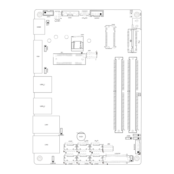
Page 7: Motherboard Layout
BIELK-PAT User’s Manual 1.4 Motherboard Layout Top View Chapter 1: Introduction | 7... - Page 8 Back View » » represents the 1st pin. 8 | Chapter 1: Introduction...
-
Page 9: Chapter 2: Hardware Installation
BIELK-PAT User’s Manual Chapter 2: Hardware installation 2.1 Central Processing Unit (CPU) The mainboard includes an Intel® Celeron processor, and a cooler has been installed to provide sufficient cooling 2.2 Fan Headers These fan headers support cooling-fans built in the computer. The fan cable and connector may be different according to the fan manufacturer. -
Page 10: Expansion Slots
Memory Capacity DIMM Socket Location DDR4L Module Total Memory Size DIMM1 4GB/8GB/16GB/32GB Max is 32GB 2.4 Expansion Slots M2_1: M.2 (Key M) Slot NGFF CONN H8.5XL80MM KEY M • The M.2 slot supports M.2 Type 2242 module. When installing M.2 module, please place the screw and hex pillar to correct position. -
Page 11: Headers / Connectors
BIELK-PAT User’s Manual 2.5 Headers / Connectors F_USB1: WAFER 2X5 2MM N9-S Pin Assignment VCC5 VCC5 HUB2_USBN4 HUB2_USBN5 HUB2_USBP4 HUB2_USBP5 DUMMY PIN JW_FP: WAFER 2X5 2MM N10-S AIH Pin Assignment HDD_LED+ HDD_LED- SYS_RST_N VCC5 POWER_LED+ POWER_LED- PWRBTN F_AUDIO1: HEADER 2X4 N6... - Page 12 JSPK1: BOX 1X4 2mm-AIH-1 Pin Assignment SPKLN SPKLP SPKRP SPKRN INVERTER: WAFER 1X6 2mm W-AIH-1 Pin Assignment VCC_BL VCC_BL ENABKL_ LBKLT_CTL 12 | Chapter 2: Hardware installation...
- Page 13 BIELK-PAT User’s Manual LVDS/EDP: SMD WAFER 2X15 1.25MM-AIH-1 Pin Assignment LVDSB_DATA3_N LVDSB_DATA3_P LVDSB_CLK_N LVDSB_CLK_P LVDSB_DATA2_N LVDSB_DATA2_P LVDSB_DATA1_N LVDSB_DATA1_P LVDSB_DATA0_N LVDSB_DATA0_P LVDSA_DATA3_P LVDSA_DATA3_N LVDSA_CLK_P LVDSA_CLK_N LVDSA_DATA2_P LVDSA_DATA2_N LVDSA_DATA1_P LVDSA_DATA1_N LVDSA_DATA0_P LVDSA_DATA0_N PVDD2 PVDD2 PVDD2 PVDD2 JDIO: HEADER 2X5 2MM S-AIH Pin Assignment...
- Page 14 SATAPW: BOX 1X4 2.5MM-AIH-1 Pin Assignment VCC5 VCC12 DCIN1: PHOENIX CONN 2P Pin Assignment VCC(9V ~ 24V) JCOM1, JCOM2, JCOM3, JCOM4: WAFER 2X5 2MM N10-S Pin Assignment COM1C_DCD COM1C_RXD COM1C_TXD COM1C_DTR COM1C_DSR COM1C_RTS COM1C_CTS COM1C_RI 14 | Chapter 2: Hardware installation...
- Page 15 BIELK-PAT User’s Manual Edp( 與 LVDS/EDP connector 共用 ): SMD WAFER 2X15 1.25MM-AIH-1 Pin Assignment eDP_AUXP eDP_AUXN eDP_TX0P eDP_TX0N eDP_TX1P eDP_TX1N EDP_HPD PVDD2 PVDD2 PVDD2 PVDD2 JSPI: HEADER 2X5 2MM N10 S-AIH Pin Assignment SPI_WP_N VCC3.3 SPI_CS0_N_R SPI_CLK_R SPI_MISO_R SPI_MOSI_R...
-
Page 16: Jumpers / Slot
2.6 Jumpers / Slot Jumper Setting The illustration shows how to set up jumpers. When the jumper cap is placed on pins, the jumper is “close”, if not, that means the jumper is “open”. Pin opened Pin closed Pin 1-2 closed JCMOS: Clear CMOS Jumper Placing the jumper on pin2-3 allows user to restore the BIOS safe setting and the CMOS data. - Page 17 BIELK-PAT User’s Manual JLV1 JLV1 VCC5 JLV1(1-2) VCC3_3 JLV1(2-3) (Default) JLV2 JLV2 VCC12 JLV2(1-2) (Default) VCC5 JLV2(2-3) JPUSB1 JPUSB1 VCC5 JPUSB1(2-3) (Default) VCC5A JPUSB1(1-2) Chapter 2: Hardware installation | 17...
- Page 18 JPDIO1 JPDIO1 VCC5 JPDIO1(1-2) (Default) VCC3_3 JPDIO1(2-3) JPOWER1 JPOWER1 JPOWER1(1-2) (Default) JPOWER1(2-3) COMPWR COMPWR VCC12 COMPWR(1-2) VCC5 COMPWR(2-3) 18 | Chapter 2: Hardware installation...
- Page 19 BIELK-PAT User’s Manual COMPWR1 COMPWR1 VCC12 JLV1(1-2) VCC5 JLV1(2-3) SATA1: SATA CONNECTOR-B Pin Assignment SSATA_TXP1 SSATA_TXN1 SSATA_RXN1 SSATA_RXP1 SCAN1: NANO SIM 6P Lift Pin Assignment SIM_PWR_B UIM_RESET UIM_CLK SIM_VPP UIM_DATA Chapter 2: Hardware installation | 19...
- Page 20 SCAN2: M.2 H4.8MM KEY B Pin Assignment Assignment M2_B_CFG3 +V3.3A +V3.3A FULL_CARD_PWROFF 6 USB2_P3_DP USB2_P3_DN M2_B_CFG0 USB3_P3_RX_DN USB3_P3_RX_DP UIM_RESET UIM_CLK USB3_P3_TX_DN UIM_DATA USB3_P3_TX_DP SIM_PWR_B M2_B_DEVSLP PCIE_RX2_DN PCIE_RX2_DP PCIE_TX2_DN PCIE_TX2_DP PLTRST_N PCIE_REFCLK1_DN PCIE_CLKREQ1_N PCIE_REFCLK1_DP WAKE_N M2_WWAN_RST_N SIM_DET M2_B_CFG1 SUSCLK_M2B +V3.3A +V3.3A M2_B_CFG2 +V3.3A 20 | Chapter 2: Hardware installation...
- Page 21 BIELK-PAT User’s Manual PE1: Mini PCIe Connector MINI PCIE 9.9H SLOT Pin Assignment Assignment WAKE_N +V3.3A +V1P5A SIM_PWR_B1 UIM_DATA1 11 PCIE_REFCLK3_DN UIM_CLK1 13 PCIE_REFCLK3_DP UIM_RESET1 15 GND SIM_VPP1 17 NC 19 NC 3G_DISABLE 21 GND PCIRST1_N 23 PCIE_RX3_DN +V3.3A 25 PCIE_RX3_DP...
- Page 22 LED2/LED3: Power LED LED No. Function LED Color LED2 Standby LED3 Power On Blue 22 | Chapter 2: Hardware installation...
Need help?
Do you have a question about the BIELK-PAT and is the answer not in the manual?
Questions and answers