
Related Manuals for VIA Technologies SOM-7000


Summary of Contents for VIA Technologies SOM-7000
- Page 1 USER MANUAL VIA SOM-7000 Fanless and low-power Edge AI platform with MediaTek Genio 1200 Octa-Core processor 1.00-26092023...
- Page 2 VIA Technologies, Inc. reserves the right the make changes to the products described in this manual at any time without prior notice.
- Page 3 VIA SOM-7000 User Manual Battery Recycling and Disposal • Only use the appropriate battery specified for this product. • Do not re-use, recharge, or reheat an old battery. • Do not attempt to force open the battery. • Do not discard used batteries with regular trash.
- Page 4 Octa-Core SoC, 16GB eMMC, 4GB LPDDR4 SDRAM, CSI, audio 2.2GHz/2.0GHz (headphone out and MIC-in), Wi-Fi 6+ Bluetooth 5.2, 3 Wi-Fi/ Bluetooth antenna I-PEX connectors VIA SOM-7000 starter kit with VIA SOM-7000 module, VIA STK-SOM700-00A0 SOMDB7 reference carrier board and accessory kit Optional Accessories...
-
Page 5: Table Of Contents
VIA SOM-7000 User Manual Table of Contents Product Overview ............................1 Key Features ............................1 Product Specifications ........................... 2 Layout Diagram ............................. 4 Product Dimensions ..........................4 Height Distribution ..........................5 Onboard I/O Connectors ..........................6 4-Lane MIPI CSI Connector ........................6 I-PEX Antenna Connectors ........................ - Page 6 VIA SOM-7000 User Manual SOMDB7 Onboard Jumpers ........................ 39 A.7.1 Watchdog Jumper ........................40...
- Page 7 VIA SOM-7000 User Manual List of Figures Figure 01: Layout diagram of the VIA SOM-7000 module's top layer ..............4 Figure 02: Dimensions of the VIA SOM-7000 module ..................4 Figure 03: Height distribution on the VIA SOM-7000 module's top layer ............5 Figure 04: MIPI CSI connector 'CSI3' ........................
- Page 8 VIA SOM-7000 User Manual List of Tables Table 01: MIPI CSI connector 'CSI3' pinouts ....................... 7 Table 02: Audio-out connector 'AUDIO_CON' pinouts ..................9 Table 03: MicroSD card slot pinouts ......................... 17 Table 04: USB 3.1 pinouts ..........................17 Table 07: Gigabit LAN port LED color definition ....................
-
Page 9: Product Overview
SoC for deep learning, neural network acceleration, and computer vision applications, including facial recognition, object identification, and OCR. Measuring just 8.2cm x 8cm (3.22" x 3.15"), the VIA SOM-7000 Edge AI module features onboard 4GB LPDDR4 SDRAM and 16GB eMMC flash memory. Multimedia capabilities include support for hardware-accelerated H.265/H.264 4K video processing, headphone-out and MIC-in, as well as multiple MIPI/HDMI/LVDS displays... -
Page 10: Product Specifications
VIA SOM-7000 User Manual 1.2 Product Specifications Processor • MediaTek Genio 1200 Octa-Core SoC − Four Cortex-A78 @ 2.2GHz − Four Cortex A55 @ 2.0GHz System Memory • 4GB LPDDR4 SDRAM Storage • 16GB eMMC Flash Memory Graphics • ARM Mali-G57 MCS High Performance GPU •... - Page 11 VIA SOM-7000 User Manual • 1 x SPI • 2 x I • • 2 x UART • 1 x single-lane PCIe • 1 x SD card • 1 x 5V DC-in Onboard I/O • 1 x MIPI CSI connector •...
-
Page 12: Layout Diagram
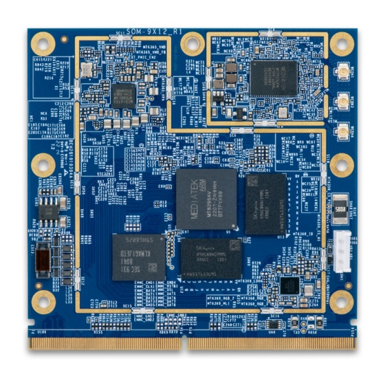
MediaTek Genio 1200 Octa-core SoC eMMC Audio Connector MIPI CSI PMIC LPDDR4 SDRAM Figure 01: Layout diagram of the VIA SOM-7000 module's top layer 1.4 Product Dimensions 82mm 74mm 37mm 6.95mm 39mm Figure 02: Dimensions of the VIA SOM-7000 module... -
Page 13: Height Distribution
VIA SOM-7000 User Manual 1.5 Height Distribution 1.34mm 4.25mm Figure 03: Height distribution on the VIA SOM-7000 module's top layer... -
Page 14: Onboard I/O Connectors
2.1 4-Lane MIPI CSI Connector The VIA SOM-7000 module is equipped with a 4-lane MIPI CSI connector labeled 'CSI3' on the top layer, which can be used for connecting a 2-lane or 4-lane MIPI CSI camera. The pinouts of the MIPI CSI connector are shown below. -
Page 15: Table 01: Mipi Csi Connector 'Csi3' Pinouts
VIA SOM-7000 User Manual CSI3 Signal Signal XCLK 16 MCN DGND 17 DGND Reset 18 MCP MDN2 19 PAVDD 2.8V 20 DGND MDP2 21 AF AVDD 2.8V DOVDD1.8V 22 MDN0 DGND 23 AFGND AGND 24 MDP0 10 MDN3 25 DVDD 1.2V... -
Page 16: I-Pex Antenna Connectors
VIA SOM-7000 User Manual 2.2 I-PEX Antenna Connectors The VIA SOM-7000 module comes with three I-PEX antenna connectors on the top layer, labeled 'WCON1 BT' for Bluetooth, 'WCON3 WF0' for Wi-Fi MAIN, and 'WCON4 WF1' for Wi-Fi AUX. The diagram of the I-PEX antenna connectors is shown below. -
Page 17: Audio-Out Connector
The VIA SOM-7000 module is equipped with a stereo audio-out connector labeled 'AUDIO_CON' on the top layer. The audio cable bundled in the VIA SOM-7000 starter kit can be plugged into this connector and the VIA SOMDB7 reference carrier board's audio-in connector. -
Page 18: Software And Technical Support
VIA SOM-7000 User Manual 3. Software and Technical Support 3.1 Android and Yocto Support The VIA SOM-7000 features a complete software evaluation image featuring the Android 11 and Yocto 4.0.6 operating systems. 3.2 Technical Support and Assistance • For utilities downloads and the latest documentation and information about the VIA SOM-7000, please visit our website at https://www.viatech.com/en/edge/SOM-7000/. -
Page 19: Appendix Asomdb7 Carrier Board Reference
VIA SOM-7000 User Manual Appendix A SOMDB7 Carrier Board Reference A.1 SOMDB7 Specifications LVDS • Chrontel CH7515 eDP/DP to LVDS Converter Ethernet • Realtek RTL8153 GbE USB 3.0 Ethernet Network Interface Controller • STMicroelectronics STM32L011F4P6 32-bit MCU Onboard I/O •... - Page 20 VIA SOM-7000 User Manual Operating Humidity • 0% ~ 95% (relative humidity ; non-condensing) Form Factor • 151mm x 134mm (5.94" x 5.28") Compliance • CE, FCC, UKCA, TELEC...
-
Page 21: Somdb7 Layout Diagram
VIA SOM-7000 User Manual A.2 SOMDB7 Layout Diagram GPIO/ADC Header M.2 Slot 2-Lane MIPI CSI USB 3.1 4-Lane MIPI CSI Micro USB 2.0 Ethernet HDMI Power Button LVDS Reset Button Vol- Button Headphone Jack Download/Vol+ Button DC-in 4-Lane MIPI DSI... -
Page 22: Figure 09: Layout Diagram Of The Somdb7 Carrier Board's Front Panel I/O
VIA SOM-7000 User Manual MicroSD Card Slot Figure 09: Layout diagram of the SOMDB7 carrier board's front panel I/O 2x Gigabit LAN HDMI Reset Button 2x USB Power Button Headphone Jack Micro USB Figure 10: Layout diagram of the SOMDB7 carrier board's back panel I/O... -
Page 23: Somdb7 Dimensions
VIA SOM-7000 User Manual A.3 SOMDB7 Dimensions 142.79mm 5.84mm 5.46mm 140.51mm 151mm Figure 11: Dimensions of the SOMDB7 carrier board 24.93mm 17.19mm 97.63mm Figure 12: Dimensions of the SOMDB7 carrier board's front panel I/O 133.24mm 115.73 mm 98.08mm 76.23mm 56.21mm 41.32mm... -
Page 24: Somdb7 Height Distribution
VIA SOM-7000 User Manual A.4 SOMDB7 Height Distribution 7.2mm 15.8mm 3.1mm 16.05mm 15.37mm 9.9mm 4.3mm 1.42mm 7.8mm 7.12mm 8.5mm 4.76mm 7.7mm 4.76mm Figure 14: Height distribution on the SOMDB7 carrier board's top layer 2.95mm 1.5mm 2.5mm Figure 15: Height distribution on the SOMDB7 carrier board's bottom layer... -
Page 25: Somdb7 External I/O Pin Descriptions And Functionality
VIA SOM-7000 User Manual A.5 SOMDB7 External I/O Pin Descriptions and Functionality The VIA SOMDB7 carrier board has a wide selection of interfaces, and includes a selection of frequently-used ports as part of the external I/O coastline. A.5.1 MicroSD Slot The VIA SOMDB7 carrier board is equipped with a MicroSD Slot on the front I/O panel, to use for storage of data, pictures, video, audio, documents and so on. -
Page 26: Micro Usb 2.0 Port
VIA SOM-7000 User Manual A.5.3 Micro USB 2.0 Port The VIA SOMDB7 carrier board is equipped with a Micro USB 2.0 port on the back panel, to be used for OS image downloading. The pinouts of the Micro USB 2.0 port are shown below. -
Page 27: Hdmi® Port
VIA SOM-7000 User Manual A.5.5 HDMI® Port The VIA SOMDB7 carrier board is equipped with an HDMI type A port on the back panel, which uses an HDMI port Type A receptacle connector to connect High Definition video and digital audio using a single cable. The port supports HDMI 2.0. -
Page 28: Reset Button
VIA SOM-7000 User Manual A.5.7 Reset Button The VIA SOMDB7 carrier board comes with a reset button on the back panel to be used for reboots or force- reset. The diagram of the reset button is shown below. Figure 22: Reset button diagram A.5.8 Headphone Jack... -
Page 29: Somdb7 Onboard I/O
VIA SOM-7000 User Manual A.6 SOMDB7 Onboard I/O This chapter provides information about the onboard I/O connectors and pin headers of the VIA SOMDB7 carrier board. A.6.1 MXM 3.0 Connector The VIA SOMDB7 carrier board comes with one 314-pin MXM 3.0 connector labeled ‘U37’. The MXM 3.0 connector is used for connecting the SOM module. - Page 30 VIA SOM-7000 User Manual Signal Signal CSI1_RX2- CSI0_RX1+ CSI1_RX3+ CSI0_RX1- CSI1_RX3- S16 - S33 GBE0_MDI3- GBE0_MDI3+ S35 - S37 GBE0_LINK100# AUDIO_MCK GBE0_LINK1000# I2S0_LRCK GBE0_MDI2- GBE0_MDI2+ I2S0_SDIN GBE0_LINK_ACT# I2S0_CK GBE0_MDI1- S43 - S46 GBE0_MDI1+ I2C_GP_CK GBE0_MDI0- I2C_GP_DAT GBE0_MDI0+ I2S2_LRCK I2S2_SDOUT SDIO_WP...
- Page 31 VIA SOM-7000 User Manual Signal Signal P62 - P64 PCIE_B_REFCK+ USB0+ PCIE_B_REFCK- USB0- P62 - P64 PCIE_B_RX+ USB1+ PCIE_B_RX- USB1- PCIE_B_TX+ PCIE_B_TX- P69 - P71 USB_TYPEC_CC1 DP0_LANE0+ USB_TYPEC_CC2 DP0_LANE0- DP0_LANE1+ P75 - P76 DP0_LANE1- PCIE_B_CKREQ# DP0_HPD DP0_LANE2+ S100 DP0_LANE2- P80 - P81...
-
Page 32: Table 10: Mxm 3.0 Connector 'U37' Pinouts
VIA SOM-7000 User Manual Signal Signal P108 GPIO0 S125 DSI0_D0+ P109 GPIO1 S126 DSI0_D0- P110 GPIO2 S127 LCD0_BKLT_EN P111 GPIO3 S128 DSI0_D1+ P112 GPIO4 S129 DSI0_D1- P113 GPIO5 S130 P114 GPIO6 S131 DSI0_D2+ P115 GPIO7 S132 DSI0_D2- P116 GPIO8 S133... -
Page 33: Audio-In Connector
The VIA SOMDB7 carrier board is equipped with a stereo audio-in connector labeled 'AUDIO_CON' on the top layer. The audio cable bundled in the VIA SOM-7000 starter kit can be plugged into this connector and the VIA SOM-7000 module's audio-out connector. -
Page 34: Lvds Connectors
VIA SOM-7000 User Manual A.6.3 LVDS Connectors The VIA SOMDB7 carrier board is equipped with two dual-channel LVDS connectors labeled 'LVDS1' and 'LVDS2' to support upto 8 lanes of data transfer to a connected QSXGA 60Hz LVDS display. The connectors are located on the top layer. -
Page 35: Lvds Backlight Connector
VIA SOM-7000 User Manual LVDS2 Signal Signal Signal 1 - 4 TXC3N TXD3P 5 - 6 TXC2N TXD2P TXA3N TXC3P 35 - 36 GND TXA2N TXC2P TXE3N TXA3P 23 - 24 GND TXE2N TXA2P TXCK3N TXE3P 11 - 12 GND... -
Page 36: 4-Lane Mipi Dsi Connector
VIA SOM-7000 User Manual A.6.5 4-Lane MIPI DSI Connector The VIA SOMDB7 carrier board is equipped with a 4-lane MIPI DSI panel connector labeled 'JDSI1' on the top layer, which can be used for connecting a MIPI DSI LCD display. The pinouts of the MIPI DSI connector are shown below. -
Page 37: 4-Lane Mipi Csi Connector
VIA SOM-7000 User Manual A.6.6 4-Lane MIPI CSI Connector The VIA SOMDB7 reference carrier board is equipped with a 4-lane MIPI CSI connector labeled 'CSI1' on the top layer, which can be used for connecting a 2-lane or 4-lane MIPI CSI camera. The pinouts of the MIPI CSI connector are shown below. -
Page 38: Table 16: Mipi Csi Connector 'Csi1' Pinouts
VIA SOM-7000 User Manual CSI1 Signal Signal XCLK 16 MCN DGND 17 DGND Reset 18 MCP MDN2 19 PAVDD 2.8V 20 DGND MDP2 21 AF AVDD 2.8V DOVDD1.8V 22 MDN0 DGND 23 AFGND AGND 24 MDP0 10 MDN3 25 DVDD 1.2V... -
Page 39: 2-Lane Mipi Csi Connector
VIA SOM-7000 User Manual A.6.7 2-Lane MIPI CSI Connector The VIA SOMDB7 carrier board comes with a 2-lane MIPI CSI connector labeled 'CSI2' on the top layer. The connector can be used for connecting a 2-lane MIPI CSI camera. The pinouts of the connector are shown below. -
Page 40: Touchscreen Panel Connector
VIA SOM-7000 User Manual A.6.8 Touchscreen Panel Connector The VIA SOMDB7 carrier board comes with a touchscreen panel connector labeled 'JTOUCH1' on the top layer. The connector supports the I C interface and can be used to connect a touchscreen panel. The pinouts of the touchscreen connector are shown below. -
Page 41: Volume Buttons
VIA SOM-7000 User Manual A.6.9 Volume Buttons The VIA SOMDB7 carrier board comes with two volume buttons for volume control. The volume-up and volume-down buttons are labeled as 'SW2' and 'SW1' respectively. The volume-up button 'SW2' is also the download key, which can be pressed to start an OS image download. -
Page 42: Dc-In Power Connector
The VIA SOMDB7 carrier board comes with a DC-in power connector labeled 'J7' on the top layer. The power cable bundled in the VIA SOM-7000 starter kit can be plugged into this connector and connected to a 12V 3A power adapter. The pinouts of the DC-in power connector are shown below. -
Page 43: Gpio/Adc Expansion Header
VIA SOM-7000 User Manual A.6.11 GPIO/ADC Expansion Header The VIA SOMDB7 carrier board comes with a GPIO/ADC expansion header labeled as 'JGPIO' on the top layer. The GPIO/ADC header supports three GPIO pins. Pins GPIO1 and GPIO2 can be used for ADC in the 0V ~ 3.3V analog range. -
Page 44: M.2 Slot
VIA SOM-7000 User Manual A.6.12 M.2 Slot The VIA SOMDB7 carrier board is equipped with an M.2 format 3042 key B slot labeled 'J2' on the top layer, for wireless networking options such as a 4G LTE M.2 module. The interface is based on USB 2.0, USB 3.1, and PCIe. -
Page 45: Sim Card Slot
USIM_RST1 USIM_CLK1 UIM_VPP1 USIM_DATA1 Table 22: SIM card slot 'SIM1' pinouts Note: Refer to instructions in the VIA SOM-7000 Starter Kit Quick Start Guide for installing the optional 4G LTE M.2 wireless module kit and an activated 4G SIM card. -
Page 46: Debug Console Connector
The VIA SOMDB7 carrier board is equipped with a debug console connector labeled 'J14' on the bottom layer. The debug console cable bundled in the VIA SOM-7000 starter kit can be plugged into this connector and a developer PC to perform software debugging. The pinouts of the debug console connector are shown below. -
Page 47: Figure 37: Jumper Settings Example
VIA SOM-7000 User Manual A.7 SOMDB7 Onboard Jumpers Jumper Description A jumper consists of a pair of conductive pins used to close in or bypass an electronic circuit to set up or configure a particular feature using a jumper cap. The jumper cap is a small metal clip covered by plastic. It performs like a connecting bridge to short (connect) the pair of pins. -
Page 48: Figure 38: Watchdog Jumper Diagram
VIA SOM-7000 User Manual A.7.1 Watchdog Jumper The VIA SOMDB7 carrier board comes with a watchdog jumper labeled as 'J11'. The watchdog jumper is used to enable or disable the watchdog function on the VIA SOMDB7 carrier board. The watchdog jumper settings are shown below. - Page 49 Taiwan Headquarters Japan China 1F, 531 Zhong-zheng Road, 940 Mission Court 3-15-7 Ebisu MT Bldg. 6F, Tsinghua Science Park Bldg. 7 Xindian Dist., New Taipei City 231 Fremont, CA 94539, Higashi, Shibuya-ku No. 1 Zongguancun East Road, Taiwan Tokyo 150-0011 Haidian Dist., Beijing, 100084 Japan China...
Need help?
Do you have a question about the SOM-7000 and is the answer not in the manual?
Questions and answers