
Related Manuals for VIA Technologies SOM-6X50


Summary of Contents for VIA Technologies SOM-6X50
- Page 1 USER MANUAL SOM-6X50 Compact cost-effective solution for HMI applications with rapid time-to-market 1.02-08222018-143700...
- Page 2 VIA Technologies, Inc. reserves the right the make changes to the products described in this manual at any time without prior notice.
- Page 3 Battery Recycling and Disposal • Only use the appropriate battery specified for this product. • Do not re-use, recharge, or reheat an old battery. • Do not attempt to force open the battery. • Do not discard used batteries with regular trash. •...
- Page 4 SOM-6X50 User Manual Box Contents Items for STK-SOM6X50-00A1 • 1 x SOM-6X50 module • 1 x SOMDB1 carrier board • 1 x 7” LCD touch panel • 2 x USB cables • 1 x COM cable • 1 x speaker...
-
Page 5: Table Of Contents
Product Dimensions ..........................5 2. Onboard I/O Connector ....................6 Debug Connector ..........................6 3. Hardware Installation ......................7 Installing the SOM-6X50 Module on the SOMDB1 Carrier Board ............7 4. Software and Technical Support ..................9 Linux Support ............................9 Technical Support and Assistance......................9 Appendix A. - Page 6 Figure 2: Layout diagram of the SOM-6X50 module (bottom side) ..............4 Figure 3: Dimensions of the SOM-6X50 module (top view) ................5 Figure 4: Dimensions of the SOMDB1 carrier board with the SOM-6X50 module installed ....... 5 Figure 5: Debug connector diagram ........................6 Figure 6: Installing the thermal pad ........................7 Figure 7: Installing the SOM-6X50 module ......................
- Page 7 SOM-6X50 User Manual List of Tables Table 1: Debug connector pinouts ........................6 Table 2: LCD panel connector pinouts ......................13 Table 3: Touch connector pinouts ........................14 Table 4: USB 2.0 connectors pinouts ....................... 15 Table 5: Camera connector pinouts ........................ 15 Table 6: COM connectors pinouts ........................
-
Page 8: Product Overview
10/100Mbps Ethernet, nine GPIO, and one Micro SD Card slot. The VIA SOM-6X50 features a Linux BSP which includes the kernel (3.4.5) and bootloader source codes. Other features include a Tool Chain to help make adjustments to the kernel and to support the VIA SOMDB1 carrier board I/O and other hardware features. -
Page 9: Product Specifications
SOM-6X50 User Manual Product Specifications Processor • 800MHz VIA Cortex-A9 SoC System Memory • 512MB DDR3 SDRAM Storage • 8GB eMMC Flash Memory Boot Loader • 512KB SPI Flash ROM Graphics • Mali-400 SP GPU * Two integrated, independent 3D/2D graphics processing units * Graphics engine supporting OpenGL® ES 2.0 hardware acceleration... - Page 10 SOM-6X50 User Manual Operating System • Linux Kernel 3.4.5 Operating Temperature • 0°C ~ 60°C Operating Humidity • 0% ~ 95% (non-condensing) Form Factor • 67.6mm x 48mm (2.66” x 1.89”) Notes: 1. As the operating temperature provided in the specifications is a result of the test performed in VIA’s chamber, a number of variables can influence this result. Please note that the working temperature may vary depending on the actual situation and environment. It is highly recommended to execute a solid testing program and take all the variables into consideration when building the system. Please ensure that the system runs well under the operating temperature in terms of application. 2. Please note that the lifespan of the onboard eMMC memory chip may vary depending on the amount of access.
-
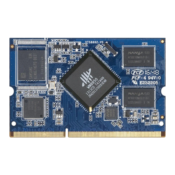
Page 11: Layout Diagram
SOM-6X50 User Manual Layout Diagram VIA Cortex-A9 SoC eMMC DDR3 SDRAM Golden finger Figure 1: Layout diagram of the SOM-6X50 module (top side) Debug connector Figure 2: Layout diagram of the SOM-6X50 module (bottom side) -
Page 12: Product Dimensions
Product Dimensions 44.3mm 48mm 67.6mm Figure 3: Dimensions of the SOM-6X50 module (top view) 41mm 42mm 26mm 100mm V T S 86 6 6 C SOMDB1 160mm Figure 4: Dimensions of the SOMDB1 carrier board with the SOM-6X50 module installed... -
Page 13: Onboard I/O Connector
SOM-6X50 User Manual 2. Onboard I/O Connector This chapter provides information about the SOM-6X50’s onboard I/O connector and its functionality. Debug Connector The SOM-6X50 comes with a debug connector which is used for debugging purposes. It supports TX/RX. The pinouts of the debug connector are shown below. Signal UART0TXD UART0RXD SFCLK SFDO... -
Page 14: Hardware Installation
Figure 6: Installing the thermal pad Step 2 Align the notch on the SOM-6X50 module with the counterpart on the SOM DDR3 SODIMM slot on the SOMDB1 carrier board then insert the module at a 30° angle. Figure 7: Installing the SOM-6X50 module... -
Page 15: Figure 8: Securing The Som-6X50 Module
SOM-6X50 User Manual Step 3 Once the SOM-6X50 module has been fully inserted, push down the module until the standoff holes align with the screw holes and then secure the module with the provided screws. Figure 8: Securing the SOM-6X50 module... -
Page 16: Software And Technical Support
SOM-6X50 User Manual 4. Software and Technical Support Linux Support The SOM-6X50 features a complete software evaluation image featuring the Linux Kernel 3.4.5 operating system. Technical Support and Assistance • For utilities downloads and the latest documentation and information about the SOM-6X50, please visit our website at https://www.viatech.com/en/boards/modules/som-6x50/ • For technical support and additional assistance, always contact your local sales representative or board distributor, or go to https://www.viatech.com/en/support/driver-support-fag/technical-support/ technical support. • For OEM clients and system integrators developing a product for long term production, other code and resources may also be made available. Please visit our website at https://www.viatech.com/en/... -
Page 17: Appendix A. Somdb1 Carrier Board Reference
SOM-6X50 User Manual Appendix A. SOMDB1 Carrier Board Reference A.1. Board Specifications Onboard I/O • 1 x LCD panel connector • 1 x Touch connector • 2 x USB 2.0 connectors • 4 x COM connectors • 2 x UART pin headers •... -
Page 18: Somdb1 Layout Diagram
SOM-6X50 User Manual A.2. SOMDB1 Layout Diagram LCD panel connector Touch connector DC-in connector Debug connector USB 2.0 connector Power bu on System recovery bu on Watchdog mer switch SOM DDR3 V T S8 666 C SOMDB1 SODIMM slot IR Receiver... -
Page 19: Figure 11: Somdb1 Front Panel I/O
SOM-6X50 User Manual Headphone jack RCA jack 10/100Mbps Ethernet Figure 11: SOMDB1 front panel I/O Micro SD card slot Figure 12: SOMDB1 back panel I/O Micro USB 2.0 OTG HDMI Figure 13: SOMDB1 right panel I/O... -
Page 20: Somdb1 Onboard I/O
SOM-6X50 User Manual A.2.1. SOMDB1 Onboard I/O A.2.1.1. LCD Panel Connector The SOMDB1 carrier board provides a 18/24-bit single-channel LCD panel connector labeled as “J34” which is used for connecting the LVDS LCD display. The pinouts of the LCD panel connector are shown below. Signal Signal LCM_LEDA LCD_G1 LCM_LEDA LCD_G0 LCM_LEDK LCD_R7 LCM_LEDK LCD_R6 LCD_R5 VCOM... -
Page 21: Touch Connector
SOM-6X50 User Manual A.2.1.2. Touch Connector The SOMDB1 carrier board comes with a touch connector labeled as “J35” which is used for connecting the touch controller panel. The pinouts of the touch panel connector are shown below. Signal DRIVE15 DRIVE14 DRIVE13 DRIVE12 DRIVE11 DRIVE10 DRIVE09 DRIVE08 DRIVE07 DRIVE06 VTS866 6C SOMDB1 DRIVE05 DRIVE04 DRIVE03 DRIVE02 Figure 15: Touch connector diagram... -
Page 22: Usb 2.0 Connector
SOM-6X50 User Manual A.2.1.3. USB 2.0 Connector The SOMDB1 carrier board has two USB 2.0 connectors which are used for connecting USB devices. The connectors are labeled as “J2” and “J4”. The pinouts of the USB 2.0 connectors are shown below. Signal Signal VBUS01 VBUS01 USBH2- USBH1- VTS8666C USBH2+ SOMDB1 USBH1+ Table 4: USB 2.0 connectors pinouts Figure 16: USB 2.0 connectors diagram... -
Page 23: Com Connector And Uart Pin Header
SOM-6X50 User Manual A.2.1.5. COM Connector and UART Pin Header The SOMBD1 carrier board is equipped with four COM connectors labeled as “J55”, “J57”, “J58” & “J59”, and two UART pin headers labeled as “J8” and “J9”. The COM connectors support the RS-232 standard while the UART pin headers are used to attach additional ports for serial devices that support TX/RX, RTS, CTS and debugging TX/RX. -
Page 24: Gpio Pin Header
SOM-6X50 User Manual A.2.1.6. GPIO Pin header The SOMBD1 carrier board comes with a GPIO pin header labeled as “J20” which supports up to 9 GPI and 9 GPO signals. The 9 inputs and 9 outputs signals can be programmed to read or control devices, with input or output defined. The pinouts of the GPIO pin header are shown below. -
Page 25: I 2 C Pin Header
SOM-6X50 User Manual A.2.1.8. C Pin header The SOMDB1 carrier board comes with an I²C pin header labeled as “J18”which is used for connecting to I²C devices. The pinouts of the I²C pin header are shown below. Signal Signal VCC33 VCC33 I2C1SCL I2C1SDA I2C2SCL I2C2SDA I2C3SCL I2C3SDA Table 10: I C pin header pinouts VTS866 6C SOMDB1 Figure 21: I C pin header diagram A.2.1.9. -
Page 26: Mic-In Connector
SOM-6X50 User Manual A.2.1.10. Mic-In Connector The SOMDB1 carrier board comes with a Mic-in connector that supports a microphone. A cable must be used to connect the devices to the connector. The Mic-in connector is labeled as “J42”. The pinouts of the Mic-in connector are shown below. -
Page 27: Audio Mono Out Signal Pin Header
SOM-6X50 User Manual A.2.1.12. Audio Mono Out Signal Pin Header The SOMDB1 carrier board is equipped with an audio mono out signal pin header which is used for connecting external audio amplifier. The audio mono out signal pin header is labeled as “J25”. The pinouts of the audio mono out signal pin header are shown below. Signal OUT3 Table 14: Audio mono out signal pin header pinouts V TS 8 6 6 6 C SOMDB1 Figure 25: Audio mono out signal pin header diagram A.2.1.13. -
Page 28: Right Channel Speaker Connector & Pin Header
SOM-6X50 User Manual A.2.1.14. Right Channel Speaker Connector & Pin Header The SOMDB1 carrier board is equipped with a right channel speaker connector & pin header for the right speaker respectively. The right channel speaker connector is labeled as “J22” and the pin header as “J23”. The pinouts of the right channel speaker connector & pin headers are shown below. -
Page 29: Ir Receiver Sensor & Pin Header
SOM-6X50 User Manual A.2.1.16. IR Receiver Sensor & Pin Header The SOMDB1 carrier board is equipped with an IR receiver sensor & pin header which are used for connecting IR devices to the board. The IR receiver sensor is labeled as “IR1” and the pin header as “J16”. The pinouts of the IR receiver are shown below. Signal... -
Page 30: Power Button
SOM-6X50 User Manual A.2.1.18. Power Button The SOMBD1 carrier board comes with a power button labeled as “SW1” which supports the on and off function of the system. The diagram of the power button is shown below. VTS8666 C SOMDB1 Figure 31: Power button diagram A.2.1.19. System Recovery Button The SOMBD1 carrier board comes with a system recovery button labeled as “SW2” which reboots and recovers the system when it crashes or turns off. The diagram of the system recovery button is shown below. VT S8666C SOMDB1 Figure 32: System recovery button diagram A.2.1.20. Watchdog Timer Switch The SOMDB1 carrier board comes with a watchdog timer switch labeled as “SW3” which enables and disables the watchdog function on the board. The diagram of the watchdog timer switch is shown below. Disable Disable VT S8 666C SOMDB1 Enable Enable Figure 33: Watchdog timer switch diagram... -
Page 31: Rca Pin Header
SOM-6X50 User Manual A.2.1.21. RCA Pin Header The SOMBD1 carrier board comes with a RCA pin header which is used for connecting the display using component video signals. The RCA pin header is labeled as “J45”. The pinouts of the RCA pin header are shown below. Signal CVBS_IN Table 20: RCA pin header pinouts VTS8 666C SOMDB1 Figure 34: RCA pin header diagram A.2.1.22. -
Page 32: Dc-In Connector
SOM-6X50 User Manual A.2.1.23. DC-In Connector The SOMDB1 carrier board comes with a DC-in connector that carries a 5V ~ 19V DC which provides power to the board. The connector is labeled as “J46”. The pinouts of power DC-in connector are shown below. -
Page 33: Som Ddr3 Sodimm Slot
A.2.1.24. SOM DDR3 SODIMM Slot The SOMDB1 carrier board comes with a SOM DDR3 SODIMM slot labeled as “J1”. The SOM DDR3 SODIMM slot is only used for installing the SOM-6X50 module. The pinouts of the SOM DDR3 SODIMM memory slot are shown below. -
Page 34: Table 23: Som Ddr3 Sodimm Slot Pinouts
SOM-6X50 User Manual Signal Signal Signal Signal 161 RINPUT1 162 SPI1SS0- nLCD1CLK- VDOUT6 163 RINPUT2 164 SPI1MISO VDOUT13 165 GND 166 GPIO1 nLCD1DO0+ VDOUT9 167 WAKEUP3 168 GPIO0 nLCD1DO0- VDOUT7 169 PWRENVCC 170 GPIO6 VDOUT15 171 WAKEUP2 172 GPIO3 nLCD1D01+... -
Page 35: Somdb1 External I/O
SOM-6X50 User Manual A.2.2. SOMDB1 External I/O The SOMDB1 carrier board has a wide selection of interfaces. It includes a selection of frequently used ports as part of the external I/O coastline. A.2.2.1. HDMI Port ® The SOMDB1 carrier board has an HDMI port on the right panel. The HDMI port uses a Type A receptacle connector to connect high definition video and digital audio using a single cable. The pinouts of the HDMI port are shown below. -
Page 36: 10/100Mbps Ethernet Port
SOM-6X50 User Manual A.2.2.3. 10/100Mbps Ethernet Port The SOMDB1 carrier board comes with a 10/100Mbps Ethernet port which uses an 8 Position 8 Contact (8P8C) receptacle connector commonly referred to as RJ-45. It is fully compliant with IEEE 802.3 (10BASE-T) and 802.3u (100BASE-TX). The pinouts of the 10/100Mbps Ethernet port are shown below. Signal Figure 40: 10/100Mbps Ethernet port diagram... -
Page 37: Micro Sd Card Slot
SOM-6X50 User Manual A.2.2.5. Micro SD Card Slot The SOMDB1 carrier board comes with a Micro SD card slot located on the back panel with support for a maximum storage capacity of 32GB. The pinouts of the Micro SD card slot are shown below. -
Page 38: Somdb1 Dimensions
SOM-6X50 User Manual A.3. SOMDB1 Dimensions 41mm 77mm 42mm 3.8mm 26mm 100mm 92.4mm VTS86 66C SOMDB1 3.8mm 152.4mm 160mm Figure 44: Dimensions of the SOMDB1 carrier board 115.5mm 84mm 16mm 1.7mm Figure 45: Dimensions of the SOMDB1 front panel I/O... - Page 39 Taiwan Headquarters Japan China 1F, 531 Zhong-zheng Road, 940 Mission Court 3-15-7 Ebisu MT Bldg. 6F, Tsinghua Science Park Bldg. 7 Xindian Dist., New Taipei City 231 Fremont, CA 94539, Higashi, Shibuya-ku No. 1 Zongguancun East Road, Taiwan Tokyo 150-0011 Haidian Dist., Beijing, 100084 Japan China...
Need help?
Do you have a question about the SOM-6X50 and is the answer not in the manual?
Questions and answers