Table of Contents
Advertisement
Quick Links
Advertisement
Table of Contents

Related Manuals for CHAINTECH 7VJL5


Summary of Contents for CHAINTECH 7VJL5
- Page 1 7VJL5 AMD Socket A VIA KT400A + VT8235 ATX Motherboard User’s Guide Version 1.0...
- Page 2 According to 47 CFR, Parts 2 and 15 of the FCC Rules The following designated product: EQUIPMENT: MAINBOARD MODEL NO.: 7VJL5 is a Class B digital device that complies with 47 CFR Parts 2 and 15 of the FCC Rules. Operation is subject to the following two conditions: 1.
- Page 3 Federal Communications Commission Statement This device complies with FCC Rules Part 15. Operation is subject to the following two conditions: * This device may not cause harmful interference. * This device must accept any interference received, including interference that may cause undesired operation. This equipment has been tested and found to comply with the limits for a Class B digital device, pursuant to Part 15 of the FCC Rules.
-
Page 4: Table Of Contents
TABLE OF CONTENTS Introduction ..............1 Chapter 1 1-1 Product Specifications.................... 1 1-2 Package Contents ....................1 1-3 7VJL5 Motherboard Layout................... 2 Hardware Setup..............3 Chapter 2 2-1 Installing a CPU Processor for Socket A ............... 3 2-2 Setting Your CPU’s Performance................4 2-3 Main Memory Configuration ................. -
Page 5: Chapter 1 Introduction
Chapter 1 Introduction Chapter 1 1-1 Product Specifications Processor Supports AMD Socket A Athlon XP/Athlon/Duron CPU Supports system clock at 200/266/333 MHz Chipset VIA KT400A + VT8235 Main Memory Supports three 184 pin DDR DIMMs up to 3GB Supports PC 2100/2700/3200 DDR SDRAM modules Expansion Slots One Universal AGP slot for both 4X/8X AGP Five 32-Bit PCI slots (v2.2 compatible) -
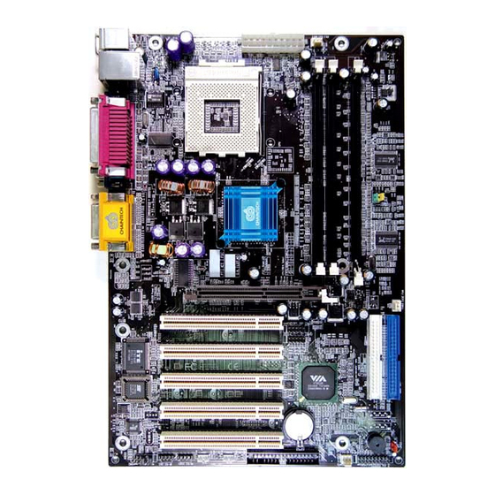
Page 6: 7Vjl5 Motherboard Layout
Chapter 1 1-3 7VJL5 Motherboard Layout... -
Page 7: Chapter 2 Hardware Setup
Chapter 2 Hardware Setup Chapter 2 If your motherboard has already been installed in your computer you may still need to refer to this chapter if you plan to upgrade your system's hardware. This motherboard is electrostatic sensitive. Do not touch without wearing proper safety gadget and make sure to disconnect the power cable from the power source before performing any work on your motherboard. -
Page 8: Setting Your Cpu's Performance
Chapter 2 2-2 Setting Your CPU’s Performance Frequency Configuration: If you install a CPU on this motherboard, you must set the [Front Side Bus Frequency] JP3 according to your processor. * CPU Speed = Multiplier x FSB Frequency AMD (K7) Duron CPU Micron Model CPU Speed Multiplier Vcore... - Page 9 Chapter 2 1400 1400MHz 14.0 1.75V 256KB 0.18 1000 1000MHz 1.75V 256KB 0.18 1113 1113MHz 1.75V 256KB 0.18 1200 1200MHz 1.75V 256KB 0.18 1333 1333MHz 10.0 1.75V 256KB 0.18 1400 1400MHz 10.5 1.75V 256KB 0.18 AMD Athlon XP CPU (Palomino/Thoroughbred) Micron Model CPU Speed...
-
Page 10: Main Memory Configuration
Chapter 2 2-3 Main Memory Configuration The DDR SDRAM memory system consists three banks, each bank supports up to 1GB of memory. DDR SDRAM Specifications Memory Internal System BUS Frequency Frequency 133 MHz 266 MHz 166 MHz 333 MHz 200 MHz 400 MHz DIMM type: 2.5V, unbuffered 184 pin 64/128/265/512-bit DDR SDRAM. -
Page 11: Connector And Jumper Settings
Chapter 2 2-4 Connector and Jumper Settings Connectors are used to link the system board with other parts of the system, including the power supply, the keyboard, and the various controllers on the front panel of the system case. The power supply connector is the last connection to be made while installing a motherboard. - Page 12 Chapter 2 button on your ATX case, or by enabling the Power Management and Suspend Mode options in BIOS's Power Management menu. (See section 3.5) Poly-fuse Over Current Protection The poly-fuse protects the system from dangerous voltages that the system might be exposed to via the keyboards or USB connectors.
- Page 13 Chapter 2 trickle, the CPU clock is stopped, and the CPU core is in its minimum power state. The system is activated whenever the keyboard or mouse is touched. The system resumes in different ways as defined by Power Management Setup screen in BIOS. 4.
- Page 14 Chapter 2 connector is used for connecting 40 pins of ATAPI devices. IDE 1 only connects two IDE devices. (Primary Master/Slave) IDE 2 only connects two IDE devices. (Secondary Master/Slave) JP1 (CMOS Clear Jumper) Definition 1-2 Normal (default) 2-3 Clear CMOS Data There is a CMOS RAM on board that has a power supply from external battery to keep the data and system configuration.
- Page 15 Chapter 2 JP6 (Enable/Disable USB 0/1 Device Wake-Up Jumper) Definition Disable (default) Enable An USB keyboard hot key or an USB mouse click can activate this board. To use this function, select a hot key of your choice at the USB Resume from S3 option under Wake Up Events in the BIOS's Power On Management screen.
- Page 16 Chapter 2 CN2/CN2A (CD-ROM Audio-in Connector) Use the audio cable enclosed with your CD-ROM disk drive to connect the CD-ROM to your motherboard. This will enable your CD-ROM's audio function. CN5 [WOL (Wake-on-LAN) Connector] Enable the Wake Up On LAN selection in BIOS's Power Management Menu to use this function.
- Page 17 Chapter 2 CN5A [WOM (Wake-on-Modem) Connector] Enable the Wake Up On Modem selection in BIOS's Power Management Menu to activate this function. This header is used to connect an add-in modem card, which gives WOM capability to the motherboard. CN23/CN23A (Front USB Connector for USB 2/3 and 4/5) USB Port 2/3 CN23, USB Port 4/5...
- Page 18 Chapter 2 CN24 (Front Audio Connector) This connector gives you the option of a front-panel audio jack cable ext. to be plugged into a special custom-designed system case. Simply remove the two jumper caps at pin [5-6] and [9-10] then plug it into the (optional) cable ext.
-
Page 19: Chapter 3 Bios Setup Program
Chapter 3 BIOS Setup Program Chapter 3 Phoenix-Award BIOS ROM has a built-in setup program that allows users to modify the basic system configuration. This information is stored in CMOS RAM so that it can retain the setup information, even when the power is turned off. To enter the Phoenix-Award BIOS setup program press [Delete] when you Power on or reboot the computer system. -
Page 20: Standard Cmos Setup
Chapter 3 3-1 Standard CMOS Setup The Standard CMOS Setup allows users to configure system components such as hard disk drive, floppy disk drive and video display as well as date, time and boot-up error signaling. This configuration menu should be changed when installing a motherboard for the first time, changing hardware in your system such as the HDD, FDD, video display, or when the CMOS data was lost or corrupted. -
Page 21: Advanced Bios Features
Chapter 3 Halt On When the system is powered on, BIOS performs a series of diagnostic tests called POST (Power On Self Test). This function stops the computer if BIOS detects a hardware error. You can tell BIOS to halt on all errors, no errors, or not to halt on specific errors. 3-2 Advanced BIOS Features By choosing the Advanced BIOS Features option from the CMOS Setup Utility menu (Figure 3-1), the screen below is displayed. - Page 22 Chapter 3 CPU L2 Cache ECC Checking Enable this function for the CPU L2 Cache Error Checking and Correcting (ECC) operation. Quick Power On Self Test Enable this function to reduce the amount of time required to run the POST (Power On Self Test).
- Page 23 Chapter 3 3. Typematic Delay (Msec) The typematic delay sets how long after you press a key that a character begins repeating. Security Option The Supervisor and/or User Password functions shown in Figure 3-1 must be set to take advantage of this function. See Section 3.11 for password setting information. When the Security Option is set to System, a password must be entered to boot the system or enter the BIOS setup program.
-
Page 24: Advanced Chipset Features
Chapter 3 Show POST CODE Enabling this function can show POST error code on the screen before proceeding to operating system. 3-3 Advanced Chipset Features By choosing the [Advanced Chipset Features] option from the CMOS Setup Utility menu (Figure 3-1), the screen below is displayed. This sample screen contains the manufacturer's default values for the motherboard. - Page 25 Chapter 3 AGP & P2P Bridge Control 1. AGP Aperture Size This feature allows users to select the size of the AGP aperture. It also determines the maximum amount of system RAM that can be allocated to the graphics card for texture storage.
- Page 26 Chapter 3 is enabled, you must set the DRAM timing function to 60ns or 70ns, depending on the type of DRAM you install. System BIOS Cacheable Enabling this function allows caching of the system BIOS ROM at F0000h-FFFFFh, resulting in better system performance. However, if any program writes to this memory area, a system error may result.
-
Page 27: Integrated Peripherals
Chapter 3 3-4 Integrated Peripherals This section provides information on setting peripheral devices. By choosing the Integrated Peripherals option from the CMOS Setup Utility menu (Figure 3-1), the screen below is displayed. This sample screen contains the manufacturer's default values for the motherboard. - Page 28 Chapter 3 5. IDE HDD Block Mode Block mode is also called block transfer, multiple commands, or multiple sector read/write. If your IDE hard drive supports block mode, select Enabled to auto-detect the optimal number of block read/writes per sector. VIA OnChip PCI Device This section provides information for setting the on-board devices.
- Page 29 Chapter 3 2. Onboard Serial Port 1/2 Select an address and corresponding interrupt for the first and second serial ports. Available options are [3F8/IRQ4], [2E8/IRQ3], [3E8/IRQ4], [2F8/IRQ3], [Disabled], and [Auto]. 3. Onboard Parallel Port Select a logical LPT port address and corresponding interrupt for the physical parallel port.
-
Page 30: Power Management Setup
Chapter 3 3-5 Power Management Setup This section provides information on the Green PC power management functions. By choosing the Power Management Setup option from the CMOS Setup Utility menu (Figure 3-1), the screen below is displayed. This sample screen contains the manufacturer's default values for the motherboard. - Page 31 Chapter 3 Video Off Option This setting allows you to select the power-saving modes during which the monitor goes blank. Video Off Method This function serves as both a screen saver and power saver for monitors. See the next function, Video Off After, for setting the video timer. 1.
- Page 32 Chapter 3 3. PS2MS Wakeup from S3/S4/S5 This function allows the PS/2 mouse to activate the system from S3/S4/S5 power saving modes. Available Options: [Disabled] and [Enabled]. 4. USB Resume from S3 When enabled, the system is able to resume from S3 mode by a USB keyboard hot key or mouse click.
-
Page 33: Pnp/Pci Configurations
Chapter 3 3-6 PNP/PCI Configurations This section provides IRQ and DMA setting information. By choosing the PNP/PCI Configuration option from the CMOS Setup Utility menu (Figure 3-1), the screen below is displayed. This screen contains the manufacturer's default values for the motherboard. Figure 3-7 PNP OS Installed If you want to install a PNP compatible OS (such as Windows 95) , then set it to Yes. -
Page 34: Frequency/Voltage Control
Chapter 3 FDD IRQ Can Be Free This function allows user to choose if the FDD IRQ can be freed up. The default setting is [Yes] and this does not allow the IRQ to be free. 3-7 Frequency/Voltage Control By choosing the Frequency/Voltage Control option from the CMOS Setup Utility menu (Figure 3-1), the screen below is displayed. -
Page 35: Load Fail-Safe Defaults
Chapter 3 3-8 Load Fail-Safe Defaults Load Fail-Safe Defaults loads the default BIOS values directly from the CMOS Setup Utility menu (Figure3-1). If the stored record created by the setup program becomes corrupted and therefore unusable, these defaults will be loaded automatically when you turn on the computer. -
Page 36: Exit Without Saving
Chapter 3 3-12 Exit Without Saving Selecting this option and pressing Y followed by [Enter] lets you exit the Setup program without recording any new values or changing old ones. -
Page 37: Chapter 4 Driver Setup
Chapter 4 DRIVER Setup Chapter 4 Insert the support CD that come with your motherboard into your CD-ROM driver or double-click the CD drive icon in [My computer] to open the setup screen. 4-1 VIA Service Pack Setup 1. Click [VIA Service Pack] 2. - Page 38 Chapter 4 3. Please select [Yes] to accept the license agreement. 4. Please select [Next >] to continue.
- Page 39 Chapter 4 5. Please select [Next >] to continue. 6. Please select [Next >] to continue installing VIA PCI IDE Bus Driver.
- Page 40 Chapter 4 7. Please select [Next >] to continue installing AGP Driver. 8. Please select [OK] to restart your computer.
-
Page 41: Audio Driver Setup
Chapter 4 4-2 Audio Driver Setup 1. Click [Audio Driver] 2. Click [Next >] to start software installation... - Page 42 Chapter 4 3. Click [Next >] to continue. 4. Please select a folder where the program will be installed and click [Next >] to proceed.
- Page 43 Chapter 4 5. Please select one folder name from existing folders list and click [Next >] to proceed. 6. Please click [Next >] to begin the file copying process.
-
Page 44: Lan Driver Setup
Chapter 4 7. Please select [OK] to complete setup. 4-3 LAN Driver Setup 1. Click [LAN Driver]... - Page 45 Chapter 4 2. Please select [Next >] to continue. 3. Please click [Finish] to complete the setup process.
-
Page 46: Usb 2.0 Driver
Chapter 4 4-4 USB 2.0 Driver 1. Click [USB 2.0 Driver] 2. Please select [Next >] to continue. - Page 47 Chapter 4 3. Please select [Next >] to continue. 4. Please select [Yes] to accept the license agreement.
- Page 48 Chapter 4 5. Please select [OK] to continue. 6. Please select [Print to File] to continue. 7. Please click [OK] to complete the setup process.
- Page 49 Chapter 4 8. Please select [Yes] for restarting computer now or [No] for restart later, then click [Finish] to complete the installation.
- Page 50 NOTE NOTE All rights are reserved for the products and corporate names/logos that appear in this manual to their original owners. We reserve all the rights to change this manual. All information is subject to change without notice.
- Page 51 How To Contact CHAINTECH How To Contact CHAINTECH Please do not hesitate to contact us if you have any problem about our products. Any opinion will be appreciated. For Asia, Africa, Australia and Pacific Island: For UK: CHAINTECH COMPUTER CO., LTD CHAINTECH UK., LTD.
Need help?
Do you have a question about the 7VJL5 and is the answer not in the manual?
Questions and answers