Advertisement
Quick Links
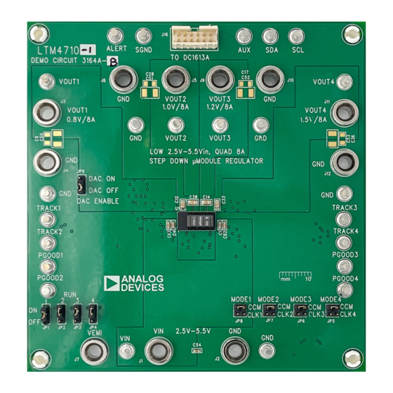
DESCRIPTION
Demonstration circuit 3164A-B features the
a quad DC/DC step-down µModule
output, packaged in a compact (6mm × 12mm × 3.54mm)
land grid array (LGA) with pre-made solder balls.
DC3164A-B has an operating input range of 2.5V to 5.5V.
The outputs of the four channels are 0.8V, 1.0V, 1.2V, and
1.5V with 8A per output, respectively. All outputs volt-
ages are programmable from 0.5V up to 3.6V (step-down
only). DC3164A-B operates by default at 1.5MHz and can
be adjusted by an external resistor from 1MHz to 5MHz or
by being synchronized to an external clock from 1.2MHz
to 2.6MHz. DC3164A-B also allows for the channels to be
paralleled up to 32A load current.
BOARD PHOTO
Low V
LTM
4710-1,
®
regulator with 8A per
®
Part marking is either ink mark or laser mark
DEMO MANUAL DC3164A-B
, Quad 8A Silent Switcher
IN
µModule Regulator
LTM4710-1 integrates four separate constant-frequency
peak current mode control regulators, power MOSFETs,
inductors, and other supporting discrete components.
It employs the second-generation Silent Switcher
technologyin which it allows fast switching edges for high
efficiency at high switching frequencies, while simulta-
neously achieving good EMI performance. Refer to the
LTM4710-1 data sheet for more detailed information.
It is recommended to read the data sheet of the LTM4710-1
prior to making any changes to the DC3164A-B board.
Design files for this circuit board are
All registered trademarks and trademarks are the property of their respective owners.
LTM4710-1
®
available.
Rev. 0
1
Advertisement

Subscribe to Our Youtube Channel
Related Manuals for Analog Devices DC3164A-B


Summary of Contents for Analog Devices DC3164A-B
- Page 1 (LGA) with pre-made solder balls. It employs the second-generation Silent Switcher ® DC3164A-B has an operating input range of 2.5V to 5.5V. technologyin which it allows fast switching edges for high The outputs of the four channels are 0.8V, 1.0V, 1.2V, and efficiency at high switching frequencies, while simulta- 1.5V with 8A per output, respectively.
- Page 2 DEMO MANUAL DC3164A-B PERFORMANCE SUMMARY Specifications are at T = 25°C, no forced-air cooling PARAMETER CONDITIONS UNITS Input Voltage Range V Default Switching Frequency Maximum Output Current For Each Channel Output Voltage of Channel 1, V OUT1 Output Voltage of Channel 2, V...
- Page 3 DEMO MANUAL DC3164A-B QUICK START PROCEDURE Figure 1. Proper Measurement Equipment Setup – Figure 2. Measuring Output Voltage Ripple Rev. 0...
- Page 4 DEMO MANUAL DC3164A-B MULTIPHASE CONFIGURATION For output loads that demand more than 8A of current, the MODE pin to become clock output used to drive the multiple LTM4710-1 channels can be paralleled to run out MODE pin of the subordinary phase(s).
- Page 5 DEMO MANUAL DC3164A-B TYPICAL PERFORMANCE CHARACTERISTICS = 2.5V = 2.5V = 3.3V = 3.3V = 5.0V = 5.0V = 5.5V = 5.5V LOAD CURRENT (A) LOAD CURRENT (A) dc3164ab F04b dc3164ab F04a (a) V = 0.8V (b) V = 1.0V...
- Page 6 DEMO MANUAL DC3164A-B TYPICAL PERFORMANCE CHARACTERISTICS 50mV/DIV 50mV/DIV LOAD STEP LOAD STEP 5A/DIV 5A/DIV dc3164ab F06a dc3164ab F06b 50 s/DIV 50 s/DIV (a) V = 0.8V (b) V = 1.0V OUT1 OUT2 50mV/DIV 50mV/DIV LOAD STEP LOAD STEP 5A/DIV 5A/DIV...
- Page 7 DEMO MANUAL DC3164A-B TYPICAL PERFORMANCE CHARACTERISTICS 50mV/DIV 50mV/DIV LOAD STEP LOAD STEP 5A/DIV 5A/DIV dc3164ab F07b dc3164ab F07a 50 s/DIV 50 s/DIV (a) V = 0.8V (b) V = 1.0V OUT1 OUT2 50mV/DIV 50mV/DIV LOAD STEP LOAD STEP 5A/DIV 5A/DIV...
- Page 8 DEMO MANUAL DC3164A-B TYPICAL PERFORMANCE CHARACTERISTICS 10mV/DIV 10mV/DIV dc3164ab F08a dc3164ab F08b 500ns/DIV 500ns/DIV (a) V = 0.8V, I = 8A (b) V = 1.0V, I = 8A OUT1 OUT1 OUT2 OUT2 10mV/DIV 10mV/DIV dc3164ab F08c dc3164ab F08d 500ns/DIV 500ns/DIV (c) V = 1.2V, I...
- Page 9 DEMO MANUAL DC3164A-B PARTS LIST ITEM REFERENCE PART DESCRIPTION MANUFACTURER/PART NUMBER Required Circuit Components C1, C3-C5, C18-C19, C47-C49, CAP ., 22µF, X5R, 10V, 20%, 0603 SAMSUNG, CL10A226MP8NUNE C54, C62-C63 CAP ., 150µF, ALUM POLY, OS-CON, 10V, 20%, PANASONIC, 10SVP150MX 8mm × 6.9mm, E7, SMD, RADIAL, SVP C8, C25-C26, C45-C46 CAP ., 0.1µF, X7R, 50V, 10%, 0603...
- Page 10 DEMO MANUAL DC3164A-B PARTS LIST ITEM REFERENCE PART DESCRIPTION MANUFACTURER/PART NUMBER Hardware for Demo Board Only E1-E18, E20-E23, E25 TEST POINT, TURRET, 0.094" MTG. HOLE, MILL-MAX, 2501-2-00-80-00-00-07-0 PCB 0.062" THK J1-J7, J9-J12 CONN., BANANA JACK, FEMALE, THT, NON-INSULATED, KEYSTONE, 575-4 SWAGE, 0.218"...
- Page 11 DEMO MANUAL DC3164A-B SCHEMATIC DIAGRAM Rev. 0...
- Page 12 DEMO MANUAL DC3164A-B SCHEMATIC DIAGRAM Rev. 0...
- Page 13 Devices for its use, nor for any infringements of patents or other rights of third parties that may result from its use. Specifications subject to change without notice. No license is granted by implication or otherwise under any patent or patent rights of Analog Devices.
- Page 14 Board until you have read and agreed to the Agreement. Your use of the Evaluation Board shall signify your acceptance of the Agreement. This Agreement is made by and between you (“Customer”) and Analog Devices, Inc. (“ADI”), with its principal place of business at One Technology Way, Norwood, MA 02062, USA. Subject to the terms and conditions of the Agreement, ADI hereby grants to Customer a free, limited, personal, temporary, non-exclusive, non-sublicensable, non-transferable license to use the Evaluation Board FOR EVALUATION PURPOSES ONLY.
Need help?
Do you have a question about the DC3164A-B and is the answer not in the manual?
Questions and answers