Yamaha MODX6 Service Manual
Hide thumbs
Also See for MODX6:
- Reference manual (218 pages) ,
- Supplementary manual (7 pages) ,
- Supplementary manual (46 pages)
Advertisement
Quick Links
MODX7
■ CONTENTS(目次)
SPECIFICATIONS(総合仕様) ...............................3/4
PANEL LAYOUT(パネルレイアウト) .......................5
CIRCUIT BOARD LAYOUT(ユニットレイアウト) ..8
DISASSEMBLY PROCEDURE(分解手順) .............10
CIRCUIT BOARDS(シート基板図) ........................20
TEST PROGRAM(テストプログラム) ..............36/53
INITIAL SETTING(出荷時の設定) ..........................69
FIRMWARE UPDATING PROCEDURES
(ファームウェアバージョンアップ) ...................70/72
SYSTEM BOOTING FLOWCHART
(起動フローチャート) ..............................................74
SY
012238
MUSIC SYNTHESIZER
MODX6
Copyright (c) Yamaha Corporation. All rights reserved. PDF TM
SERVICE MANUAL
SERVICE MANUAL
DM CIRCUIT BOARD CHECK METHOD
(DM シートチェック方法) ..................................75/76
SAVING/LOADING DATA
(本体の設定をセーブ / ロードする) ....................77/78
RESTORING THE INITIAL FACTORY SETTINGS
(工場出荷時の状態に戻す) ......................................80
DISPLAY MESSAGES(メッセージリスト) ......81/84
PARTS LIST
BLOCK DIAGRAM(ブロックダイアグラム)
WIRING(基板結線図)
CIRCUIT DIAGRAM(回路図)
HAMAMATSU, JAPAN
'18.06
Advertisement
Chapters

Related Manuals for Yamaha MODX6


Summary of Contents for Yamaha MODX6
- Page 1 (工場出荷時の状態に戻す) ........80 TEST PROGRAM(テストプログラム) ....36/53 DISPLAY MESSAGES(メッセージリスト) ..81/84 INITIAL SETTING(出荷時の設定) ......69 PARTS LIST FIRMWARE UPDATING PROCEDURES BLOCK DIAGRAM(ブロックダイアグラム) (ファームウェアバージョンアップ) ....70/72 WIRING(基板結線図) SYSTEM BOOTING FLOWCHART CIRCUIT DIAGRAM(回路図) (起動フローチャート) ..........74 012238 HAMAMATSU, JAPAN Copyright (c) Yamaha Corporation. All rights reserved. PDF TM ’18.06...
- Page 2 IMPORTANT NOTICE This manual has been provided for the use of authorized Yamaha Retailers and their service personnel. It has been assumed that basic service procedures inherent to the industry, and more specifically Yamaha Products, are already known and understood by the users, and have therefore not been restated.
- Page 3 MODX7: 1,144 (W) × 331 (D) × 134 (H) mm (45-1/16" x 13-1/16" x 5-1/4"), 7.4 kg (16 lbs 5 oz) MODX6: 937 (W) × 331 (D) × 134 (H) mm (36-7/8" x 13-1/16" x 5-1/4"), 6.6 kg (14 lbs 9 oz) Accessories AC adaptor (PA-150B or an equivalent recommended by Yamaha*), Owner’s Manual, Cubase AI...
- Page 4 16W ( 電源アダプター PA-150B 使用時 ) 寸法・質量 MODX7: 1,144 (W) × 331 (D) × 134 (H) mm、7.4kg MODX6: 937 (W) × 331 (D) × 134 (H) mm、6.6kg 付属品 電源アダプター (PA-150B またはヤマハ推奨の同等品 )、取扱説明書、保証書、 CUBASE AI DOWNLOAD INFORMATION (CUBASE AI ダウンロードについて )
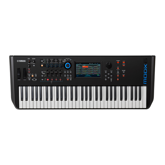
- Page 5 MODX6/MODX7 ■ PANEL LAYOUT(パネルレイアウト) Top Panel (フロントパネル) !2 !3 !2 !3 @6 @7 @6 @7 C0 D0 F0 G0 A0 B0 q Keyboard q 鍵盤 w Pitch Bend wheel w ピッチベンドホイール e Modulation wheel e モジュレーションホイール r [MASTER VOLUME] knob r [MASTER VOLUME] ( マスターボリューム...
- Page 6 MODX6/MODX7 The illustration shows a MODX8, but the information applies to all models. (イラス トは代表して MODX8 を掲載していますが、内容は同一です。 ) @3 KNOB POSITION [1] and [2] buttons @3 KNOB POSITION ( ノブポジション ) [1]、[2] ボタン @4 Super Knob @4 スーパーノブ @5 SEQ TRANSPORT button @5 シーケンサートランスポートボタン...
- Page 7 MODX6/MODX7 The illustration shows a MODX8, but the information applies to all models. Rear Panel (リアパネル) (イラス トは代表して MODX8 を掲載していますが、内容は同一です。 ) Left side of Rear Panel (リアパネル左寄り) I Right side of Rear Panel (リアパネル右寄り) •■ リアパネル左寄り •■ Left side of Rear Panel q [USB TO HOST] terminal q [USB TO HOST] 端子...
- Page 8 MODX6/MODX7 ■ CIRCUIT BOARD LAYOUT(ユニットレイアウト) MODX6 ● <UPPER CASE ASSEMBLY / 上ケース Ass y> PNL1 TOME1 TOME1 TPBZ PNL2 WHEEL ASSEMBLY SIDE PAD R SIDE PAD L (ホイール Ass y) (サイドパッド R) (サイドパッド L) <LOWER CASE ASSEMBLY / 下ケース Ass y>...
- Page 9 MODX6/MODX7 MODX7 ● <UPPER CASE ASSEMBLY / 上ケース Ass y> PNL1 TOME1 TOME1 TPBZ PNL2 WHEEL ASSEMBLY SIDE PAD R SIDE PAD L (ホイール Ass y) (サイドパッド R) (サイドパッド L) <LOWER CASE ASSEMBLY / 下ケース Ass y> KEY-IF TOME3 TOME1 TOME1 DM UPPER ANGLE (DM 上金具)...
-
Page 10: Table Of Contents
MODX6 Disassembling the Keyboard Assembly ..16 MODX6 鍵盤 Ass’ y の分解 ..... . 16 MODX7 Disassembling the Keyboard Assembly ..18 MODX7 鍵盤... - Page 11 LOWER CASE ASSEMBLY (下ケース Ass y) <Bottom view / 下面> [180] x 7 [180] x 3 [180] x 3 * This figure shows the MODX6 (この図は MODX6 です。 ) [170] x 5 Fig. 1 ( 図 1) [160] S FLEXIBLE FLAT CABLE TOME4 (S カード電線)...
-
Page 12: Circuit Boards And Assemblies (Lower Case Section)
350B PUSH KNOB(プッシュツマミ) TOME2 350C KEY-IF 350D DCIN 350E Table 1 ( 表 1) KEY-IF * This figure shows the MODX6 TOME1 TOME1 (この図は MODX6 です。 ) [80] [370D] x 2 [370A] x 2 [350E] x 2 DCIN [350B] x 9 [350D] x 4 DM UPPER ANGLE (DM 上金具)... -
Page 13: Circuit Boards And Assemblies (Upper Case Section)
[570A] x 2 [550C] x 4 [550B] x 6 [550E] x 7 TPBZ [570B] x 4 PNL2 * This figure shows the MODX6 [550D] x 7 (この図は MODX6 です。 ) WHEEL ASSEMBLY SIDE PAD R SIDE PAD L (ホイール Ass y)... -
Page 14: Pnr Circuit Board
(Fig. 6) PNC シート交換時には、新しい基板に取り付けてください。 The shade cushion is not part of the PNC circuit board. Install it to the new circuit board when replacing the PNC circuit board. * This figure shows the MODX6 [30] [50] [90] [70] (この図は MODX6 です。 )... -
Page 15: Lcd Display
MODX6/MODX7 LCD Display 液晶ディスプレイ (Time required: About 6 minutes) (所要時間:6 分) 6-1. 上ケース Ass’ y を外します。 (1 項参照) 6-1. Remove the upper case assembly. (See procedure 1) 6-2. TOME1 シートを外します。 (3 項参照) 6-2. Remove the TOME1 circuit board. (See procedure 3) 6-3. -
Page 16: Modx6 Disassembling The Keyboard Assembly
MODX6/MODX7 MODX6 Disassembling the Keyboard MODX6 鍵盤 Ass’ y の分解 Assembly 7-1. 下ケース Ass’ y を外します。 (1 項参照) 7-1. Remove the lower case assembly. (See procedure 1) 7-2. 7-2. White Keys and Black Keys 白鍵、黒鍵 7-2-1. [120A] のネジ 4 本を外して、鍵盤補強金具 2 個を... - Page 17 MODX6/MODX7 KEYBOARD ANGLE KEYBOARD ANGLE (鍵盤補強金具) (鍵盤補強金具) [120A] x 2 [120B] [120A] x 2 [120B] x 2 [120B] x 4 [120B] x 3 [120B] x 3 [120B] x 4 B1 C2 B2 C3 B3 C4 B4 C5 ONE OCTAVE ONE OCTAVE...
-
Page 18: Modx7 Disassembling The Keyboard Assembly
MODX6/MODX7 Fig. 11 ( 図 11) MODX7 Disassembling the Keyboard MODX7 鍵盤 Ass’ y の分解 8-1. 下ケース Ass’ y を外します。 (1 項参照) Assembly 8-1. Remove the lower case assembly. (See procedure 1) 8-2. 白鍵、黒鍵 8-2. White Keys and Black Keys 8-2-1. [240A] のネジ 4 本を外して、鍵盤補強金具 2 個を... - Page 19 MODX6/MODX7 KEYBOARD ANGLE KEYBOARD ANGLE (鍵盤補強金具) (鍵盤補強金具) [240A] x 2 [240A] x 2 [240B] x 2 [240B] x 3 [240B] x 4 [240B] x 3 [240B] x 3 [240B] x 4 [240B] x 3 B1 C2 B2 C3 B3 C4 B4 C5 (E0–B0)
- Page 20 MODX6/MODX7 ■ CIRCUIT BOARDS(シート基板図) 61H Circuit Board (X2335D0) ....................33 61L Circuit Board (X2336C0) ....................32 76H Circuit Board (XJ095B0) ....................35 76L Circuit Board (XJ096B0) ....................34 DCIN Circuit Board (YJ417D0) ....................30 DM Circuit Board (YJ337C0) ....................22/23 JK Circuit Board (YJ417D0) .....................
- Page 21 MODX6/MODX7 JK Circuit Board to PNC-CB100 to DM-CB605 -CB605 to PNL1-CB109 to PNL1-CB110 Component side(部品側) 2NA-ZX99470...
- Page 22 MODX6/MODX7 DM Circuit Board to JK-CB102 to LCD Component side(部品側) 2NA-ZW84620...
- Page 23 MODX6/MODX7 DM Circuit Board Pattern side(パターン側) 2NA-ZW84620...
- Page 24 MODX6/MODX7 PNC Circuit Board Component side(部品側) 2NA-ZX42110...
- Page 25 MODX6/MODX7 PNC Circuit Board to JK-CB401 to PNL1-CB108 to PB & MW to PNL2-CB111 Pattern side(パターン側) 2NA-ZX42110...
- Page 26 MODX6/MODX7 PNL1 Circuit Board to PNC-CB102 to JK-CB301 to JK-CB201 Component side(部品側) Pattern side(パターン側) KEY-IF Circuit Board MODX6: to 61H-CN2 MODX7: N.C. MODX6: to 61L-CN5 MODX6: to 61H-CN1 MODX7: N.C. MODX7: to 76L-CN4 MODX6: N.C. MODX6: N.C. MODX7: to 76L-CN5 MODX7: to 76H-CN1 Component side(部品側)...
- Page 27 MODX6/MODX7 PNL2 Circuit Board TPBZ Circuit Board to LCD to DM-CB101 Component side(部品側) Component side(部品側) to PNC-CB103 Pattern side(パターン側) PNL2: 2NA-ZX42110 TPBZ: 2NA-ZX99490 (MODX6) 2NA-ZX99480 (MODX7)
- Page 28 MODX6/MODX7 PNR Circuit Board Component side(部品側) 2NA-ZX42110...
- Page 29 MODX6/MODX7 PNR Circuit Board to PNC-CB107 Pattern side(パターン側) 2NA-ZX42110...
- Page 30 MODX6/MODX7 DCIN Circuit Board TOME1 Circuit Board Component side(部品側) to JK-CB101 Component side(部品側) TOME2 Circuit Board TOME3 Circuit Board Component side(部品側) Component side(部品側) DCIN, TOME1, TOME2, TOME3: 2NA-ZX99490 (MODX6) 2NA-ZX99480 (MODX7)
- Page 31 MODX6/MODX7 TOME4 Circuit Board Pattern side(パターン側) Component side(部品側) 2NA-ZX42110...
- Page 32 MODX6/MODX7 61L Circuit Board ● ● 2NAK8-V869520...
- Page 33 MODX6/MODX7 61H Circuit Board ● ● to KEY-IF-CB503 to 61L-CN4 to KEY-IF-CB505 E’ E’ to KEY-IF-CB505 Component side(部品側) 2NAK8-V869540...
- Page 34 MODX6/MODX7 76L Circuit Board ● ● F’ F’ Component side(部品側) 2NAK8-ZW58970...
- Page 35 MODX6/MODX7 76H Circuit Board ● ● to 76L-CN3 G’ to KEY-IF-CB508 H’ G’ H’ Component side(部品側) 2NAK8-ZW58960...
- Page 36 MODX6/MODX7 ■ TEST PROGRAM * If you execute Test No. 24 Factory Set, the setting data and user data will be lost. Be sure to save these data for backup in advance. (See page 77.) 1. Measurement condition 1-1. Environment Perform tests under following conditions.
- Page 37 MODX6/MODX7 2. Test mode 2-1. Starting up Test mode There are two methods to start up Test mode. Method 1 While pressing keys [C#2], [F2], [G#2] (C#2 major chord) simultaneously, turn on the [ ] (Standby/On) switch. Method 2 While pressing the buttons [KNOB POSITION 1] and [CONTROL ASSIGN] simultaneously, turn on the [ ] (Standby/On) switch.
- Page 38 MODX6/MODX7 2-2. Start-up screen When the Test mode is started, the start-up screen appears on the LCD which enables to check the Firmware version. TEST MODX Test Program Firm X.XX.X Kernel X.XX.XX-XXXXXX.XX.X [ENTER] : Test Start [STORE] : Factory Set [EXIT] : Exit Pressing the [ENTER] button: to enter the test item selection mode.
- Page 39 MODX6/MODX7 3. Test program list LCD display Test items and judging conditions 01 : EBUS ID Check Checks the connection condition and the key type of each EBUS IC (PNC: IC101, KEY). 1) Press the [ENTER] button, and then the result is shown on the LCD.
- Page 40 MODX6/MODX7 LCD display Test items and judging conditions 05 : Knob Checks whether USB Volume, AsgnKnobs 1 to 4 and SuperKnob work properly or not. 1) Press the [ENTER] button. The target value of each knob are shown on the LCD.
- Page 41 MODX6/MODX7 LCD display Test items and judging conditions 06 : Slider Checks whether the Sliders (Control Sliders) 1 to 4 work properly or not. 1) Press the [ENTER] button. The target value “ <127> ” of each sliders are shown on the LCD.
- Page 42 MODX6/MODX7 LCD display Test items and judging conditions 08 : FC1/2, Sus/FS Checks whether [FOOT CONTROLLER 1,2], FOOT SWITCH [ASSIGNABLE] and FOOT SWITCH [SUSTAIN] jacks work properly or not. 1) Connect the foot controller 1 (FC7) to the [FOOT CONTROLLER 1] and/or the [FOOT CON- TROLLER 2] jack.
- Page 43 MODX6/MODX7 LCD display Test items and judging conditions 11 : USB (to DEVICE) Checks whether the USB TO DEVICE terminal works properly or not. 1) Press the [ENTER] button first. “ Insert USB Memory! ” is shown on the LCD.
- Page 44 MODX6/MODX7 LCD display Test items and judging conditions 14 : OUTPUT-R (-12dB) Checks each output level from the R channel of the jacks. 1) Connect the frequency counter to the PHONES jack at R. 2) Connect the level meter to an output jack.
- Page 45 MODX6/MODX7 LCD display Test items and judging conditions 16 : A/D -> D/A (LINE) Checks the signal path from the A/D input to D/A output. (Gain is set to LINE due to Default.) 1) Connect the level meter to [OUTPUT] jack.
- Page 46 MODX6/MODX7 LCD display Test items and judging conditions 19 : ROM Checks eMMC (IC403), SUB CPU ROM (IC502) and WAVE ROM (IC601, IC604, IC605, IC607). (This check takes about 11 seconds.) 1) Press the [ENTER] button, and then the result is shown on the LCD.
- Page 47 MODX6/MODX7 LCD display Test items and judging conditions 24 : Factory Set Sets to the factory default data. (It takes about 8 seconds.) After writing the initial value of each parameter in the SDRAM, those data is written to the eMMC (IC403).
- Page 48 MODX6/MODX7 LCD display Test items and judging conditions 29 : OUTPUT-L (-6dB) Checks each output level from the L channel of the jacks. 1) Connect the level meter to an output jack. 2) Set the [MASTER VOLUME] control to the maximum position.
- Page 49 MODX6/MODX7 LCD display Test items and judging conditions 33 : Panel C Check (SW, Checks whether switches and LEDs on the PNC circuit board work properly or not. LED) 1) Press the [ENTER] button, and “ Press KNOB FUNCTION / LED=ORANGE ” is shown on the LCD.
- Page 50 MODX6/MODX7 4. Other Inspections (Check in Usual mode) Test Item Instructions Popping noise Checks whether the popping noise is output properly or not when the power is turning on and off. 1) Connect the Oscilloscope to the output jacks. (Connect the plugs to both L and R output jacks at the same time.) 2) Set the [MASTER VOLUME] to the maximum position.
- Page 51 MODX6/MODX7 03: Panel Switch, LED (Switch Test Sequence) ● Order SW Name LED Name Order SW Name LED Name color color STORE ORANGE STORE ASSIGN 1 ASSIGN 1 AUDITION ORANGE AUDITION ASSIGN 2 ASSIGN 2 SHIFT ORANGE SHIFT MS HOLD...
- Page 52 MODX6/MODX7 33: Panel C Check (SW, LED) (Switch Test Sequence) 34: Panel R Check (SW, LED) (Switch Test Sequence ) ● ● Order SW Name LED Name Order SW Name LED Name color color KNOB FUNCTION ORANGE KNOB FUNCTION DEC/NO...
- Page 53 MODX6/MODX7 ■ テストプログラム ※テストナンバー 24 の Factory Set を実行すると、設定データ及びユーザーデータが失われます。 事前にデータバックアップを行ってください。 (78 ページ参照) 1. 測定条件 1-1. 環境 以下の状態で行います。 常温 (温度 5℃~ 40℃) 常湿 (湿度 20% ~ 90%) 但し、検査基準をはずれた場合は常温 (温度 5℃~ 40℃) 、常湿 (相対湿度 30% ~ 90%)で再測定して ください。 1-2. 電源電圧 AC アダプターは、PA-150B を使用します。...
- Page 54 MODX6/MODX7 1-7. 測定単位 アナログ入出力レベル単位は、0 dBu = 0.775Vrms とします。 2. テストモード 2-1. テストモードの起動 テス トモードの起動方法は 2 種類あります。 方法 1 1) 鍵盤の [C#2]、[F2]、[G#2] ( C#2 メジャーコード)を押しながら [ ] ( スタンバイ/ オン ) スイ ッチをオンにします。 方法 2 1) [KNOB POSITION 1] ボタンと [CONTROL ASSIGN] ボタンを同時に押しながら [ ] ( スタンバイ/ オン...
- Page 55 MODX6/MODX7 2-2. スタート画面 1) テストモードが起動されると、 LCD に “TEST”モード起動画面が表示されます。ファームウェアのバージョンが確認で きます。 TEST MODX Test Program Firm X.XX.X Kernel X.XX.XX-XXXXXX.XX.X [ENTER] : Test Start [STORE] : Factory Set [EXIT] : Exit [ENTER] ボタンを押すとテス ト項目選択画面に移動します。 [STORE] ボタンを押すと Factory Set テス ト選択画面に移動します。 [EXIT] ボタンを押すと Exit テス ト選択画面に移動します。...
- Page 56 MODX6/MODX7 3. テスト一覧 LCD 表示 テスト項目及び判定条件 01 : EBUS ID Check 各 EBUS IC (PNC: IC101, KEY) の接続状態と Key Type をチェックします。 1) [ENTER] ボタンを押すと LCD に結果が表示されます。 OK の場合: OK NG の場合: NG 2) LCD に“OK”が表示されることを確認します。 3) テスト結果の OK/NG が表示された時点で、テストが終了して項目選択状態となります。 02 : LCD, LED LCD、全...
- Page 57 MODX6/MODX7 LCD 表示 テスト項目及び判定条件 05 : Knob USB Volume, AsgnKnob 1-4, SuperKnob が正常に動作することを確認します。 1) [ENTER] ボタンを押すと LCD に各ノブの目標値が表示されます。 チェックする Knob の順番に指定はありません。 USB Volume 2) LCD に USB Volume の目標値“< 127 >”が表示されます。 3) LCD の表示に従って、目標値(127)までゆっくりと上げます。 現在値が 0 から 127 までスムーズに増えることを確認します。 4) 現在値 125 ~ 127 を検知すると、表示が目標値“< 0 >”に切替ります。...
- Page 58 MODX6/MODX7 LCD 表示 テスト項目及び判定条件 06 : Slider Slider(コントロールスライダー)1 ~ 4 が正常に動作することを確認します。 1) [ENTER] ボタンを押すと LCD に各 slider の目標値“< 127 >”が表示されます。 チェックする Slider の順番に指定はありません。 2) Slider 1 から Slider 4 を LCD の表示に従って、目標値(127)までゆっくりと上げます。 現在値が 0 から 127 までスムーズに増えることを確認します。 3) 現在値 125 ~ 127 を検知すると、表示が目標値“< 0 >”に切替ります。...
- Page 59 MODX6/MODX7 LCD 表示 テスト項目及び判定条件 08 : FC1/2, Sus/FS [FOOT CONTROLLER 1, 2]、FOOT SWITCH [ASSIGNABLE]、FOOT SWITCH [SUSTAIN] 端子が 正常に動作することを確認します。 1) フットコントローラー (FC7) のペダルを踏み込んだ状態で、[FOOT CONTROLLER 1] 及び [FOOT CONTROLLER 2] 端子に接続します。 2) FOOT SWITCH [SUSTAIN] 端子は接続しません。 3) FOOT SWITCH [ASSIGNABLE] 端子にフットスイッチペダル (FC4A/FC5) を接続します。...
- Page 60 MODX6/MODX7 LCD 表示 テスト項目及び判定条件 11 : USB (to DEVICE) USB TO DEVICE 端子が正常に動作することを確認します。 1) [ENTER] ボタンを押すと LCD に“Insert USB Memory!”が表示されます。 フラッシュメモリー 2) USB を挿入します。 3) LCD に“OK”が表示されることを確認します。 4) テスト結果の OK/NG が表示された時点で、テストが終了して項目選択状態となります。 フラッシュメモリー 5) USB を外します。 12 : USB (to HOST) USB TO HOST 端子が正常に動作することを確認します。...
- Page 61 MODX6/MODX7 LCD 表示 テスト項目及び判定条件 15 : A/D -> D/A (MIC) A/D 入力から D/A 出力までの信号経路をテストします。(Default で Gain は LINE になっています ) 1) [OUTPUT] 端子にレベルメーターを接続します。 (L/MONO 及び R の両端子にプラグを接続す ること。 ) 2) [MASTER VOLUME] を最大にします。 3) [ENTER] ボタンを押すと、LCD に“L-Channel input OFF”が表示されます。 4) A/D INPUT [R] 端子に残留ノイズ測定用モノプラグ(150 Ω抵抗終端)を挿入します。...
- Page 62 MODX6/MODX7 LCD 表示 テスト項目及び判定条件 17 : MUTE (Analog) アナログ回路の MUTE 機能をチェックします。 1) 測定する出力端子にレベルメーターを接続します。 2) [MASTER VOLUME] を最大にします。 3) [ENTER] ボタンを押すと、正弦波が L, R チャンネル同レベルで発音され、LCD に“OFF”が 表示されます。 4) [ENTER] ボタンを押すとミューティング回路が動作し、LCD が“ON”に切替ります。 全出力端子がミュートされることを確認します。 5) [ENTER] ボタンを押すとミューティング回路が切れ、LCD が“OFF”に切替ります。 全出力端子のミュートが外れることを確認します。 6) MUTE ON 時の出力レベルをチェックします。 出力レベルを測定し、規定範囲内であることを確認します。...
- Page 63 MODX6/MODX7 LCD 表示 テスト項目及び判定条件 21 : Internal Audio SWP70 - SSP2 間の Audio 用信号線に正常な信号が出力されていることを確認します。 本体より Audio 出力 8 系統に対してフルスケールの 441Hz 正弦波を全 ch 出力し、 SSP2 で 2ch ごと、 2 通りの結線(全 4 パターン)を順次切り替えます。 1) [ENTER] ボタンを押すと、 LCD に“Audio 1 ON”が表示され、 441 Hz の正弦波が発音します。...
- Page 64 MODX6/MODX7 LCD 表示 テスト項目及び判定条件 26 : Exit テストモードから抜けて、電源を OFF します。 1) [ENTER] ボタンを押すと、LCD に“[NO] or [YES]”が表示されます。 2) [INC/YES] ボタンを押すと、テストが終了して電源を OFF します。 ※ [DEC/NO] ボタンを押すと、TEST モード起動画面に戻ります。 3) [STANDBY/ON] スイッチを ON にして、再起動します。 通常モードのライブセット画面が表示されることを確認します。 注:ライブセット画面が表示されるまでは電源を切らないでください。 27 : OUTPUT-L (0dB) 出力端子の L チャンネルに信号を出力します。出力レベルを測定します。 1) 測定する出力端子にレベルメーターを接続します。...
- Page 65 MODX6/MODX7 LCD 表示 テスト項目及び判定条件 31 : Panel L1 Check (SW, PNL1 シートの SW および LED が正常に動作することを確認します。 LED) 1) [ENTER] ボタンを押すと LCD に “Press AD INPUT ON/OFF / LED=ORANGE” が表示されます。 2) 該当するボタンを押すと、押している間正弦波が発音します 。 ボタンに LED がある場合は LED が点灯します。 ※指定以外のボタンを押したときは“NG”が表示され発音しません。 3) ボタンを離すと、 “OK”が表示されます。...
- Page 66 MODX6/MODX7 4. その他のテスト項目 (通常モードにて確認) テスト項目 手順 Popping noise 電源 ON/OFF によるポップノイズをチェックします。 1) 測定する出力端子にオシロスコープを接続します。 (各出力端子とも、L, R 両出力端子同時に プラグを接続する。 ) 2) [MASTER VOLUME] を最大にします。 3) [STANDBY/ON] スイッチをオン/オフさせて、ノイズレベルをオシロスコープで確認します。 各出力端子のノイズが下記規定範囲内であることをチェックします。 [PHONES] (33 Ω負荷) PHONES L :≦ 500 mVp-p PHONES R :≦ 500 mVp-p [OUTPUT] (10k Ω負荷)...
- Page 67 MODX6/MODX7 03 : Panel Switch, LED(スイッチテスト順) ● 順番 スイッチ名 LED の色 LED 名前 順番 スイッチ名 LED の色 LED 名前 AUDITION ORANGE AUDITION ASSIGN 1 ASSIGN 1 SHIFT ORANGE SHIFT ASSIGN 2 ASSIGN 2 MS HOLD MS HOLD ARP ON/OFF ORANGE ARP ON/OFF...
- Page 68 MODX6/MODX7 33 : Panel C Check (SW,LED) ( スイッチテスト順) 34 : Panel R Check (SW,LED) ( スイッチテスト順) ● ● 順番 スイッチ名 LED の色 LED 名前 順番 スイッチ名 LED の色 LED 名前 KNOB FUNCTION ORANGE KNOB FUNCTION DEC/NO KNOB FUNCTION GREEN...
- Page 69 MODX6/MODX7 ■ INITIAL SETTING(出荷時の設定) • [STANDBY/ON] SW: • [MASTER VOLUME]: • A/D INPUT [GAIN]: • [USB MONITOR LEVEL]: Min • SLIDER 1~4: • Pitch Bend Wheel: Center • Modulation Wheel:...
- Page 70 When an error occurred while installing and if the instrument does not operate even if re-installation is executed, re- placement of the DM circuit board may be necessary. Download the version upgrade program from the Yamaha website. • File Name 8Q86OS_.PGM Copy the above file in the top directory of the USB flash drive in advance.
- Page 71 MODX6/MODX7 Once “Searching for the updater...OK” appears on the screen, installation startes. Also the Super Knob flickers in red during installation. Super Knob When installation is completed, the Super Knob flickers in blue. Also “Finish./Please turn off.” appears on the screen.
- Page 72 MODX6/MODX7 ■ ファームウェアバージョンアップ • 作業上の注事事項 1) 作業前にバージョンアッププログラムに付属する手順及びリリースノートの内容を確認し、その手順に従って作業を行っ て ください。 2) バージョンア ップにより現在機器内に保存されているデーターが消去されますので、データーを事前にバックア ップしてお いて ください。 3) インス トール中に USB フラッシュメモリーを抜かないでください。 4) インス トール中に電源を切らないでください。特に、インス トール開始直後に電源を切るとブー ト プログラムが破損するお それがあります。 5) インス トールに失敗したときは、画面に “Press [INC/YES] to retry.”と表示されます。[INC/YES] ボタンを押し、再 度インス トール作業を行って ください。 6) インス トール途中にエラーが発生し、再度インス トールを行っても正常に完了しない場合は DM シートの交換が必要な場...
- Page 73 MODX6/MODX7 3) 画面に “Searching for the updater...”が表示されたらボタン より手を離します。 4) “Searching for the updater...OK”の表示でインス トールが開始されます。インス トール中は [ スーパー ノブ ] が赤色で点 滅します。 スーパーノブ 5) [ スーパー ノブ ] が青色の点滅に変わり、画面に “Finish. / Please turn off.”が表示されたらインス トール完了です。 6) 電源を切り、USB フラッシュメモリーを取り外します。 7) テス ト プログラムを起動して、ファームウェアのバージョンを確認し、ファク ト リーセッ トを実施します。...
- Page 74 MODX6/MODX7 ■ SYSTEM BOOTING FLOWCHART(起動フローチャート)...
- Page 75 MODX6/MODX7 ■ DM CIRCUIT BOARD CHECK METHOD The DM Circuit Board is provided with test points for service check purposes. Check the test points on the DM Circuit Board if the following symptoms appear. Symptoms and check items Test Point ① to ④ and ⑥ sequentially No LCD display with Power SW ON -->...
- Page 76 MODX6/MODX7 ■ DM シートチェック方法 DM シートにはサービスチェック用のテストポイントを設けてあります。 下記の症状により DM シートのテストポイントを確認してください。 症状により以下の箇所を確認します。 電源を入れても LCD が点灯しない ⇒ ①~④及び⑥を順番に確認します。 テストポイントチェック NO. テストポイント 回路 判定基準 測定 GND 測定器具 不良が疑われる部品 ① デジタル回路用 5V 電源 5.0V ± 0.5V DGND テスター IC010 ② +3.3D デジタル回路用 3.3V 電源 3.3V ± 0.3V DGND テスター...
- Page 77 MODX6/MODX7 ■ SAVING/LOADING DATA Saving/Loading Data The Utility display provides tools for transferring the entire system setting and data (such as Performances and Live Sets) between the MODX and a USB flash drive connected to the [USB TO DEVICE] terminal.
- Page 78 MODX6/MODX7 ■ 本体の設定をセーブ / ロードする 本体の設定をセーブ/ロードする ユーティリティー画面では、システム全体の設定の他に本体で作成したパフォーマンス、ライブセットなどのデータをUSBフ ラッシュメモリーに保存(セーブ)したり、USBフラッシュメモリーからデータを読み込んだり(ロード)します。 ここでは、MODXのユーザーメモリー上のすべてのデータを保存(セーブ)する方法と、再度本体に読み込む(ロード)方法を説 明します。 本体の設定をUSBフラッシュメモ [Save As New File]の「+」をタッチします。 リーにセーブする NOTE すでに保存されているファイルを上書きする場合はそのファイル名 をタッチします。 USBフラッシュメモリーをMODXの[USB TO DEVICE]端子に接続します。 文字入力画面が表示され、保存するファイルの名 前を設定します。 [UTILITY]ボタンを押してユーティリティー画面 を開いたあと、画面左の[Contents]タブ → [Store/Save]タブをタッチします。 文字入力画面の「Done」を選択すると、セーブ 「Content Type」で「Backup File (バック が実行されます。 アップファイル)」を選択します。 NOTE すでに保存されているファイルを上書きする場合は、手順5のあとに コンテンツタイプを選択 実行確認の画面が表示されるので、 「YES」を選択するとセーブが実 行されます。 USBフラッシュメモリーにセーブ した本体の設定をロードする 注記 ロードを実行すると、本体に保存されていたデータは消えてしまいます。 大切なデータは、あらかじめUSBフラッシュメモリーに保存(セーブ)し ておくことをおすすめします。 保存先のUSBフラッシュメモリー、フォルダーを...
- Page 79 MODX6/MODX7 本体の設定をセーブ/ロードする USBフラッシュメモリーの取り扱いにつ USBフラッシュメモリー内のファイル(拡張子: いて .X8A)を選択して、ロードを実行します。 本機にUSBフラッシュメモリーを接続すると、楽器本体で 制作したデータをUSBフラッシュメモリーに保存したり、 USBフラッシュメモリーのデータを楽器本体で再生したり できます。 ■ 接続できるUSBフラッシュメモリーの数 同時に使用できるUSBフラッシュメモリーは、1つです。 ■ USBフラッシュメモリーのフォーマット USBフラッシュメモリーは本機でフォーマットすることを おすすめします。他の機器でフォーマットしたUSBフラッ シュメモリーは、本機で正しく動作しない場合があります。 ロード元のUSBフラッシュメモリー 注記 USBフラッシュメモリー内のロード元として、現在 フォーマットを実行すると、そのUSBフラッシュメモリーの中身は消去 設定されているフォルダー名 されます。必要なデータが入っていないのを確認してからフォーマット してください。 すでに保存されているファイルの一覧 NOTE フォーマットの方法は、リファレンスマニュアルをご参照ください。 [USB TO DEVICE]端子 ■ 誤消去防止 ご使用上の注意 USBフラッシュメモリーには、誤ってデータを消してしま わないようライトプロテクト機能のついたものがあります。 本機には[USB TO DEVICE]端子があります。[USB TO 大切なデータが入っている場合は、ライトプロテクトで書き DEVICE]端子にUSB機器を接続する場合は、以下のことを 込みができないようにしましょう。逆にデータを保存する場 お守りください。 合などは、ご使用の前にお使いのUSBフラッシュメモリー NOTE のライトプロテクトが解除されていることをご確認くださ USB機器の取り扱いについては、お使いのUSB機器の取扱説明書もご参...
- Page 80 Do not listen with the headphones at high volume for long periods of time. Doing so may cause hearing loss. age appears MODX6/MODX7 ing is retained Restoring the initial factory ■ RESTORING THE INITIAL FACTORY SETTINGS (Initialize All Data)
- Page 81 MODX6/MODX7 Display Messages ■ DISPLAY MESSAGES LCD indication Description ** will be deleted. This message appears when the specified operation you are about to execute will cause the specified data to be deleted. ** will be overwritten. This message appears when a file/folder having the same name as the one you are about to save already exists.
- Page 82 MODX6/MODX7 Display Messages LCD indication Description Library full. The maximum overall number of Libraries has been exceeded when executing the related operations. MIDI buffer full. Failed to process the MIDI data because too much data was received at one time.
- Page 83 MODX6/MODX7 Display Messages LCD indication Description USB device is full. The USB flash drive is full and no more data can be saved. Use a new USB flash drive, or make space by erasing unwanted data from the storage device.
- Page 84 MODX6/MODX7 メッセージリスト ■ メッセージリスト メッセージ 説明 ** will be deleted. 操作を実行することによりデータが削除される場合に表示されます。 セーブ時に同じ名前のファイル/フォルダ―がすでに存在している場合に表示されます。セー ** will be overwritten. ブを実行するとデータは上書きされます。**にはセーブしようとしているファイル/フォル ダー名が表示されます。 今から操作するコントローラーにパラメーターを割り当てることができます。割り当てを希 Activate the source controller to assign. 望するコントローラーを操作してください。 Advanced settings will be initialized. [Advanced]タブで行なわれた設定を初期化します。 All data and libraries will be initialized. Unsaved 工場出荷時の設定に戻します。必要なデータは、前もってUSBフラッシュメモリーに保存す...
- Page 85 MODX6/MODX7 メッセージリスト メッセージ 説明 選択したトラックや設定した範囲にデータがないときに表示されます。範囲を選びなおして No data. ください。 No read/write authority to the file. ファイルの読み取り権限および書き込み権限がありません。 工場出荷時の設定に書き換え中です。 Now initializing all data… 一部のデータ初期化中に表示されます。 Now initializing… Now loading... ファイルロード中に表示されます。 MIDIバルクデータ受信中に表示されます。 Now receiving MIDI bulk data... Now saving... ファイルセーブ中に表示されます。 Now transmitting MIDI bulk data...
- Page 86 ■ CONTENTS (目次) MODX6 OVERALL ASSEMBLY (総組立) ..........2 MODX7 OVERALL ASSEMBLY (総組立) ..........4 MODX6 UPPER CASE ASSEMBLY (上ケース Ass’ y) ......6 MODX7 UPPER CASE ASSEMBLY (上ケース Ass’ y) ......8 MODX6 LOWER CASE ASSEMBLY (下ケース Ass’ y) ......10 MODX7 LOWER CASE ASSEMBLY (下ケース...
-
Page 87: Modx6 Overall Assembly (総組立
MODX6/MODX7 ■ MODX6 OVERALL ASSEMBLY(総組立) UPPER CASE 6 ASSEMBLY: See page 6. (上ケース 6 Ass y) LOWER CASE 6 ASSEMBLY: See page 12. (下ケース 6 Ass y)... - Page 88 PART NO. DESCRIPTION 部 品 名 REMARKS REF NO. OVERALL ASSEMBLY 総 組 立 MODX6 OVERALL ASSEMBLY 総 組 立 E,B,U,Y,K,P,J,O,C (ZY79870) UPPER CASE 6 ASSEMBLY 上 ケ ー ス 6 A s s ’ y (ZY79630) LOWER CASE 6 ASSEMBLY 下...
-
Page 89: Modx7 Overall Assembly(総組立
MODX6/MODX7 ■ MODX7 OVERALL ASSEMBLY(総組立) UPPER CASE 7 ASSEMBLY: See page 8. (上ケース7Ass y) LOWER CASE 7 ASSEMBLY: See page 12. (下ケース7Ass y)... - Page 90 MODX6/MODX7 PART NO. DESCRIPTION 部 品 名 REMARKS REF NO. OVERALL ASSEMBLY 総 組 立 MODX7 OVERALL ASSEMBLY 総 組 立 E,B,U,Y,K,P,J,O,C (ZY79860) UPPER CASE 7 ASSEMBLY 上 ケ ー ス 7 A s s ’ y (ZY79620) LOWER CASE 7 ASSEMBLY 下...
-
Page 91: Modx6 Upper Case Assembly(上ケースAss' Y
MODX6/MODX7 ■ MODX6 UPPER CASE ASSEMBLY(上ケースAss’ y) WHEEL ASSEMBLY: See page 18. (ホイールAss y)... - Page 92 品 名 REMARKS REF NO. UPPER CASE ASSEMBLY 上 ケ ー ス A s s ’ y MODX6 UPPER CASE 6 ASSEMBLY 上 ケ ー ス 6 A s s ’ y (ZY79630) ZY809000 UPPER CASE 6 上 ケ ー ス 印 刷 品 6...
-
Page 93: Modx7 Upper Case Assembly(上ケースAss' Y
MODX6/MODX7 ■ MODX7 UPPER CASE ASSEMBLY(上ケースAss’ y) WHEEL ASSEMBLY: See page 18. (ホイールAss y)... - Page 94 MODX6/MODX7 PART NO. DESCRIPTION 部 品 名 REMARKS REF NO. UPPER CASE 7 ASSEMBLY 上 ケ ー ス A s s ’ y MODX7 UPPER CASE 7 ASSEMBLY 上 ケ ー ス 7 A s s ’ y (ZY79620) ZY808800 UPPER CASE 7 上...
-
Page 95: Modx6 Lower Case Assembly(下ケースAss' Y
MODX6/MODX7 ■ MODX6 LOWER CASE ASSEMBLY(下ケースAss’ y) 16N-C61 KEYBOARD: See page 14. (16N-C61鍵盤)... - Page 96 品 名 REMARKS REF NO. LOWER CASE ASSEMBLY 下 ケ ー ス A s s ’ y MODX6 LOWER CASE6 ASSEMBLY 下 ケ ー ス 6 A s s ’ y (ZY79790) ZY809400 LOWER CASE 6 下 ケ ー ス 印 刷 品 6...
-
Page 97: Modx7 Lower Case Assembly(下ケースAss' Y
MODX6/MODX7 ■ MODX7 LOWER CASE ASSEMBLY(下ケースAss’ y) 16N-E76 KEYBOARD: See page 16. (16N-E76鍵盤)... - Page 98 MODX6/MODX7 PART NO. DESCRIPTION 部 品 名 REMARKS REF NO. LOWER CASE ASSEMBLY 下 ケ ー ス A s s ’ y MODX7 LOWER CASE7 ASSEMBLY 下 ケ ー ス 7 A s s ’ y (ZY79780) ZY809300 LOWER CASE 7 下...
-
Page 99: Modx6 Keyboard Assembly(鍵盤Ass' Y
MODX6/MODX7 ■ MODX6 KEYBOARD ASSEMBLY(鍵盤Ass’ y)... - Page 100 品 名 REMARKS REF NO. KEYBOARD ASSEMBLY 鍵 盤 A s s ’ y MODX6 16N-C61 KEYBOARD 16N C61 D2 I 1 6 N - C 6 1 鍵 盤 (ZY34290) V 9 3 3 8 5 0 0 WHITE KEY 16NW C,E,G,B CEGB 白...
-
Page 101: Modx7 Keyboard Assembly(鍵盤Ass' Y
MODX6/MODX7 ■ MODX7 KEYBOARD ASSEMBLY(鍵盤Ass’ y)... - Page 102 MODX6/MODX7 PART NO. DESCRIPTION 部 品 名 REMARKS REF NO. KEYBOARD ASSEMBLY 鍵 盤 A s s ’ y MODX7 16N-E76 KEYBOARD 16N E76 D2 I 1 6 N - E 7 6 鍵 盤 (ZY34270) V 9 3 3 8 5 0 0 WHITE KEY 16NW C,E,G,B CEGB 白...
-
Page 103: Modx6/Modx7 Wheel Assembly(ホイールAss' Y
VN24540R ROTARY VARIABLE RESISTOR TOKU 10.0K RK16311 ロ ー タ リ ー V R CONNECTOR ASSEMBLY PNC-PBMW P N C - P B M W 束 線 MODX6 (ZX75870) CONNECTOR ASSEMBLY PNC-PBMW P N C - P B M W 束 線 MODX7... -
Page 104: Modx6/Modx7 Electrical Parts(電気部品
K シ ー ト MODX7 (ZX99480)(YJ417D0) VAM96100 CIRCUIT BOARD KEY-IF K E Y - I F シ ー ト MODX6 (ZX99490)(YJ417D0) VAM93900 CIRCUIT BOARD KEY-IF K E Y - I F シ ー ト MODX7 (ZX99480)(YJ417D0) VAM96200 CIRCUIT BOARD TPBZ T... - Page 105 K シ ー ト MODX7 (ZX99480)(YJ417D0) VAM96100 CIRCUIT BOARD KEY-IF K E Y - I F シ ー ト MODX6 (ZX99490)(YJ417D0) VAM93900 CIRCUIT BOARD KEY-IF K E Y - I F シ ー ト MODX7 (ZX99480)(YJ417D0) VAM96200 CIRCUIT BOARD TPBZ T...
- Page 106 N R シ ー ト MODX6/7 (ZX42110)(YJ383C0) VAM91400 CIRCUIT BOARD TOME4 T O M E 4 シ ー ト MODX6/7 (ZX42110)(YJ383C0) ZX747900 SPACER FOR LED LH-5-7.5 SHINAGAWA L E D ス ペ ー サ ー D179 ZX391100 LED GREEN SLI-343MGT32 L...
- Page 107 MODX6/MODX7 PNC/PNL1/PNL2/PNR PART NO. DESCRIPTION 部 品 名 REMARKS REF NO. SW124 WG31840R TACT SWITCH SKRGAMD010 タ ク ト S W ASSIGN2 SW125 WG31840R TACT SWITCH SKRGAMD010 タ ク ト S W MOTION SEQ HOLD SW126 WG31840R TACT SWITCH SKRGAMD010 タ...
- Page 108 RD15518R CARBON RESISTOR (CHIP) 180.0 1/4 J TP チ ッ プ 抵 抗 V869530R CIRCUIT BOARD 6 1 L シ ー ト MODX6 (V869520)(X2336C0) D001 VB941201 DIODE 1SS133,1SS176 TE-5 ダ イ オ ー ド VB941201 DIODE 1SS133,1SS176 TE-5 ダ イ...
- Page 109 MODX6/MODX7 76L and 76H PART NO. DESCRIPTION 部 品 名 REMARKS REF NO. D001 DIODE 1SS133,1SS176 TE-5 ダ イ オ ー ド (VB94121) DIODE 1SS133,1SS176 TE-5 ダ イ オ ー ド (VB94121) ZW589600 CIRCUIT BOARD 7 6 H シ ー...
- Page 110 MUSIC SYNTHESIZER CIRCUIT DIAGRAM ■ CONTENTS (目次) BLOCK DIAGRAM (ブロックダイアグラム) ..........3 WIRING (基板結線図) ................4 CIRCUIT DIAGRAM (回路図) DM (001–007) ................5–11 JK (001–004) ................12–15 KEY-IF ....................16 TPBZ, DCIN ..................17 PNC ..................... 18 PNL1, PNL2 ..................19 PNR .....................
- Page 111 MODX6/MODX7 Notation for Circuit Diagrams(回路図表記上の注意) 1. How to identify inter-sheet connectors(シート間コネクタの読み方について) C P L D _ R E S 0 0 2 : I 6 This indicates the location of the counter inter-sheet connector. (The alphabet indicates horizontal direction and the number indicates vertical direction.)
-
Page 112: Block Diagram (ブロックダイアグラム
■ BLOCK DIAGRAM(ブロックダイアグラム)(MODX6/MODX7) MODX6/MODX7 CB100 (5P) MODX6 MODX7 +3.3PN CB101 (4P) SW&LED MASTER Touch Panel MONITOR debug only INITX VOLUME SW103–121 port LEVEL (self) D145–150 VR111 SW&LED D151–155 IC101 (100P) SW132–140 KEY-IF KEY-IF CB109 (6P) D165–167 MB9AF141NA SW142–148 VR109 D177,179–208... -
Page 113: Key-If
■ WIRING(基板結線図)(MODX6/MODX7) MODX6/MODX7 * This figure shows the MODX6 (この図は MODX6 です。 ) TPBZ TOME1 MODX6 ● TOME1 WHEEL ASSEMBLY <LOWER CASE ASSEMBLY / 下ケース Ass y> (ホイール Ass y) [70] [310] [320] [U300] [350] [380] [370] 1 PIN MARK SIDE (1PIN マーク側です。 )... - Page 114 ■ DM 001 CIRCUIT DIAGRM (MODX6/MODX7) MODX6/MODX7 MICROPROCESSOR (MPU) R E S I S T O R C A P A C I T O R I C 0 0 1 P I O _ 3 . 3 V A M 3 3 5 2 B Z C Z 8 0...
- Page 115 ■ DM 002 CIRCUIT DIAGRM (MODX6/MODX7) MODX6/MODX7 S W P M _ C S N 0 0 5 : B 6 S W P S _ C S N 0 0 7 : B 6 n o _ u s e R 2 2 4 0 .
- Page 116 ■ DM 003 CIRCUIT DIAGRM (MODX6/MODX7) MODX6/MODX7 eMMC ROM 32G MAIN F I 4 0 4 V M M C R E S I S T O R R 3 4 0 9 N F E 3 1 P T 2 2 2 Z 1 E 9 L...
- Page 117 ■ DM 004 CIRCUIT DIAGRM (MODX6/MODX7) MODX6/MODX7 NOR FLASH ROM 16M REGULATOR +1.5V + 3 . 3 D + 3 . 3 D 0 . 0 1 / 1 6 ( B ) A 1 0 3 7 A K ( Q / R / S ) 0 .
- Page 118 ■ DM 005 CIRCUIT DIAGRM (MODX6/MODX7) MODX6/MODX7 NAND FLASH ROM 8G NAND FLASH ROM 8G NAND FLASH ROM 8G NAND FLASH ROM 8G SWP70 (TG MASTER) SWP70 (TG MASTER) WAVE CS0-L WAVE CS0-H WAVE CS1-L WAVE CS1-H I C 8 0 0...
- Page 119 ■ DM 006 CIRCUIT DIAGRM (MODX6/MODX7) MODX6/MODX7 R E S I S T O R C A P A C I T O R REGULATOR +1.0V R E M A R K S P A R T S N A M E...
- Page 120 ■ DM 007 CIRCUIT DIAGRM (MODX6/MODX7) MODX6/MODX7 + 3 . 3 D R P 1 3 2 S 0 0 1 D - E 2 - F not installed n o _ u s e + 1 . 0 S...
- Page 121 POWER SW CIRCUIT ■ JK 001 CIRCUIT DIAGRM (MODX6/MODX7) MODX6/MODX7 Q 1 0 2 REGULATOR +9V R R H 1 0 0 P 0 3 F I 1 0 1 D S S 1 N B 3 2 A 2 2 2 Q 9 3...
- Page 122 ■ JK 002 CIRCUIT DIAGRM (MODX6/MODX7) MODX6/MODX7 A D I N L - I N S 0 0 1 : C 6 OP AMP OP AMP J K 2 0 1 4 7 . 0 0 1 6 . 0 V R X T P...
- Page 123 ■ JK 003 CIRCUIT DIAGRM (MODX6/MODX7) MODX6/MODX7 C 3 0 1 O U T P U T - L OP AMP 0 0 1 : C 7 1 0 0 / 1 6 C B 3 0 1 N J M 4 5 8 0 M - D ( T E 2 )
- Page 124 ■ JK 004 CIRCUIT DIAGRM (MODX6/MODX7) MODX6/MODX7 + 3 . 3 P N + 3 . 3 P N J K 4 0 1 L 4 0 1 Y K F 5 1 - 5 0 6 6 V Z 4 0 1...
- Page 125 ■ KEY-IF CIRCUIT DIAGRM (MODX6/MODX7) MODX6/MODX7 5 2 1 4 7 K e y t y p e P [ 7 7 ] M K 2 3 6 1 k e y s 7 6 k e y s 8 8 k e y s...
- Page 126 ■ TPBZ, DCIN CIRCUIT DIAGRM (MODX6/MODX7) MODX6/MODX7 DCIN TPBZ + 1 2 V C B 7 0 1 J K 7 0 1 C B 6 0 1 C B 6 0 2 T H 7 0 1 0 7 F M N - S M T - A - T F (...
-
Page 127: Pnc
■ PNC CIRCUIT DIAGRM (MODX6/MODX7) MODX6/MODX7 B K 1 0 0 5 H M 6 0 1 - T C B 1 0 7 L 1 2 4 D [ 0 ] D [ 0 ] C 1 7 9... - Page 128 ■ PNL1, PNL2 CIRCUIT DIAGRM (MODX6/MODX7) MODX6/MODX7 PNL1 PNL2 D [ 4 - 8 ] L [ 4 - 5 ] C B 1 0 8 + 3 . 3 A S [ 4 - 5 ] U S B M o .
-
Page 129: Pnr
■ PNR CIRCUIT DIAGRM (MODX6/MODX7) MODX6/MODX7 D _ r e L [ 0 - 1 ] S [ 0 , 1 , 6 ] P E R F O R M A N C E L I V E S E T... -
Page 130: 61H
■ 61L, 61H CIRCUIT DIAGRM (MODX6) MODX6/MODX7 (C4 – C6) to KEY-IF-CB503 (Page 16: L-1) to KEY-IF-CB505 (Page 16: J-4) 28CC1-2001136720 (C1 – B3) to KEY-IF-CB504 (Page 16: J-3) 28CC1-2001136719 ■ 61L, 61H CIRCUIT DIAGRM (MODX6) - Page 131 ■ 76L CIRCUIT DIAGRM (MODX7) MODX6/MODX7 to 76H-CN2 (Page 23: O-8) (E0 – C3) to KEY-IF-CB503 (Page 16: L-1) 52147-1210 SW10 SW11 SW12 SW13 SW14 SW15 SW16 SW17 SW18 SW19 SW20 SW21 SW22 SW23 SW24 SW25 SW26 SW27 SW28 SW29...
- Page 132 ■ 76H CIRCUIT DIAGRM (MODX7) MODX6/MODX7 (C#3 – G6) SW34 SW35 SW36 SW37 SW38 SW39 SW40 SW41 SW42 SW43 SW44 SW45 SW46 SW47 SW48 SW49 SW50 SW51 SW52 SW53 SW54 SW55 SW56 SW57 SW58 SW59 SW60 SW61 SW62 SW63 SW64...
Need help?
Do you have a question about the MODX6 and is the answer not in the manual?
Questions and answers