Table of Contents
Advertisement
Quick Links
AT-SURF-F437 User Manual
Evaluation board with AT32F437ZMT7 MCU
Introduction
AT-SURF-F437 evaluation board with a complete set of features helps the user to explore the high
®
®
performance of the 32-bit ARM
Cortex
-M4 microcontroller AT32F437 with FPU and expedite his
application development.
AT-SURF-F437 evaluation board is based on AT32F437ZMT7 microcontroller and includes large-
capacity SDRAM, QSPI Flash and RAM, and rich peripherals (three-color LEDs, buttons, two USB
micro-B, type A connector, Ethernet RJ45 connector, digital camera moduel, microphone and audio
input and outputs, microSD card interface) and communication interfaces such as RS-232, RS-485,
two CAN transceivers, 3.5 inch TFT-LCD touch screen. All this is aimed at enabling users to
experience all the features of the AT32F437 device.
The evaluation board comes with an embedded AT-Link-EZ for debugging/programming without
the need of other development tools.
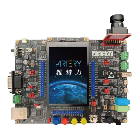
Figure 1. AT-SURF-F437 evaluation board
2022.3.24
1
Rev 1.10
Advertisement
Table of Contents

Subscribe to Our Youtube Channel
Related Manuals for ARTERY AT-SURF-F437


Summary of Contents for ARTERY AT-SURF-F437
-
Page 1: Figure 1. At-Surf-F437 Evaluation Board
AT-SURF-F437 User Manual Evaluation board with AT32F437ZMT7 MCU Introduction AT-SURF-F437 evaluation board with a complete set of features helps the user to explore the high ® ® performance of the 32-bit ARM Cortex -M4 microcontroller AT32F437 with FPU and expedite his application development. -
Page 2: Table Of Contents
AT-SURF-F437 User Manual Contents Overview ......................... 6 Features ........................6 Conventional terms ....................7 Quick start ......................8 Get started........................ 8 Hardware layout ..................... 9 Power supply ......................11 Embedded AT-Link-EZ for programming and debugging ......... 11 Boot mode selection ....................11 External clock sources ..................... - Page 3 AT-SURF-F437 User Manual 3.16.3 InfraRed receiver ......................15 3.17 Extension connector ....................15 3.18 0 Ω resistors ......................15 Pin assignment ....................16 Schematics ......................22 Revision history ....................31 2022.3.24 Rev 1.10...
- Page 4 AT-SURF-F437 User Manual List of tables Table 1. Boot mode related jumpers ....................11 Table 2. 0 Ω resistor settings ......................15 Table 3. AT32F437ZMT7 pin assignment ..................16 Table 4. Document revision history ....................31 2022.3.24 Rev 1.10...
- Page 5 AT-SURF-F437 User Manual List of figures Figure 1. AT-SURF-F437 evaluation board ..................1 Figure 2. Hardware block diagram ...................... 9 Figure 3. Top layout ........................... 10 Figure 4. Bottom layout ........................10 Figure 5. Schematic for AT-Link-EZ and power ................22 Figure 6.
-
Page 6: Overview
On-board AT-Link-EZ for programming and debugging, without the need of an emulator Power supply options: − AT-LIink-EZ USB bus − AT-SURF-F437 OTG1 or OTG2 bus (V or V BUS1 BUS2 − V can be supplied through a coin cell battery ... -
Page 7: Conventional Terms
AT-SURF-F437 User Manual Audio − Full-duplex I S2 is connected to audio codec WM8988 − Audio power amplifier-driven speaker (on the back of the board) and 3.5 mm LINE_OUT − Microphone and 3.5 mm LINE_IN Video − Digital camera module is connected to DVP interface −... -
Page 8: Quick Start
AT-SURF-F437 User Manual Quick start Get started Configure the AT-SURF-F437 evaluation board in the following order: 1. Insert camera module into the digital camera module connector CN3 with lens facing forward 2. Check the Jumper positions on the board JP2 is connected to GND or OFF (BOOT0=0. BOOT0 has a pull-down resistor in the... -
Page 9: Hardware Layout
AT-SURF-F437 User Manual Hardware layout The AT-SURF-F437 evaluation board is designed around the AT32F437ZMT7 microcontroller in a 144-pin LQFP package. Figure 2 Figure 3 illustrates the connections between the AT32F437ZMT7 and peripherals. Figure 4 Show the locations of these features on the AT-SURF-F437 evaluation board. -
Page 10: Figure 3. Top Layout
AT-SURF-F437 User Manual Figure 3. Top layout CR1220 coin microSD card slot SPI4 battery cell Camera module Exte nsion AT32F437ZMT7 AT-Link-EZ connector connector Power switch CAN2 Extension interface connector Power LED CAN1 interface C EEPROM RS-232 connector USB Type-A connector... -
Page 11: Power Supply
AT-SURF-F437 User Manual Power supply The AT-SURF-F437 evaluation board is designed to be powered by a 5 V power supply via a USB cable. It is also possible to configure the evaluation board to use the following three sources for 5 V power supply: USB connector (CN1, power switch SW1 ON) on the AT-Link-EZ;... -
Page 12: Leds
AT-SURF-F437 User Manual LEDs Power LED1 Red LED: indicates that the AT-SATRT-F437 evaluation board is being powered by 3.3 V. User LED2(RGB_LED) The Three-color LED, red, green and blue, is connected to PB10, PD13 and PB5 of the AT32F437ZMT7 respectively that adjust color change and brightness by controlling PWM duty cycle of each color. -
Page 13: Rs-232 Communication
C2. The I C address of WM8988 is 0b0011010. A 3.5 mm stereo LINE_OUT interface (CN14, light green) mounted on the AT-SURF-F437 board is linked to the output1 on the WM8988 and able to connect with a stereo playback device. A small speaker (connect to CN5 on the back of the board) is also available on the board, and it is driven by an audio power amplifier TC8002D (U17). -
Page 14: Otgfs Connector
AT32F437ZMT7 is directly connected to host via a USB micro-B cable, and either V BUS1 or V can be used to supply 5 V for the AT-SURF-F437 evaluation board. As a host, the BUS2 AT32F437ZMT7 is connected to an external device through a USB OTG cable, and the OTGFS1 and OTGFS2 provide power to the device via the USB micro-B connector by controlling SI2301 switch through IO1_5 and IO1_6 of the I/O extension connector (U21) respectively. -
Page 15: Infrared Receiver
Extension connector 3.17 The P4 and P5 of extension connector are connected to GPIOs of the AT-SURF-F437 microcontroller and can be measured through oscilloscope, logic analyzer or voltmeter. As the P6 of extension connector corresponds to CN2, it is also possible to measure and debug LCD pins via P6 when LCD is connected to CN2. -
Page 16: Pin Assignment
AT-SURF-F437 User Manual Pin assignment To offer a complete picture of the full-featured AT32F437 microcontroller, each of GPIOs on the microcontroller is presented with specific features and connected to one or more devices externally. If there is concern about the simultaneous operation of several devices controlled by the same pin, JPx or 0 Ω... - Page 17 AT-SURF-F437 User Manual Connection Connection Connection Connection Jumper or Extension Pin name Function 0 Ω resistor device1 device2 device3 device4 connector HEXT_OUT 8 MHz crystal (X2) XMC_SDNWE W9825G6KH (U6) P4[19] EMAC_MDC DM9162 (U9) P4[20] XMC_SDCS0 W9825G6KH (U6) P4[21] XMC_SDCKE0 W9825G6KH (U6)
- Page 18 AT-SURF-F437 User Manual Connection Connection Connection Connection Jumper or Extension Pin name Function 0 Ω resistor device1 device2 device3 device4 connector XMC_A11 W9825G6KH (U6) P5[38] TFT-LCD interface XMC_D4 W9825G6KH (U6) P6[10] (CN2) TFT-LCD interface XMC_D5 W9825G6KH (U6) P6[11] (CN2) TFT-LCD interface...
- Page 19 AT-SURF-F437 User Manual Connection Connection Connection Connection Jumper or Extension Pin name Function 0 Ω resistor device1 device2 device3 device4 connector TFT-LCD interface XMC_D13 W9825G6KH (U6) P6[19] (CN2) TFT-LCD interface XMC_D14 W9825G6KH (U6) P6[20] (CN2) TFT-LCD interface PD10 XMC_D15 W9825G6KH (U6)
- Page 20 AT-SURF-F437 User Manual Connection Connection Connection Connection Jumper or Extension Pin name Function 0 Ω resistor device1 device2 device3 device4 connector USART1_TX / AT-Link-EZ OTG1 interface JP1[3, 4] OTGFS1_VBUS (VCOM_RX) (CN9) R114 USART1_RX / AT-Link-EZ OTG1 interface PA10 JP1[1, 2]...
- Page 21 AT-SURF-F437 User Manual Connection Connection Connection Connection Jumper or Extension Pin name Function 0 Ω resistor device1 device2 device3 device4 connector TFT-LCD interface XMC_NE1 P6[1] (CN2) Camera interface DVP_VSYNC P5[9] (CN3) PG10 QSPI2_IO2 LY68L6400 (U8) P5[8] Camera interface PG11 DVP_D3 / PG11...
-
Page 22: Schematics
AT-SURF-F437 User Manual Schematics Figure 5. Schematic for AT-Link-EZ and power VBUS1 +3V3 DFLS130L-7 LED Red 0.1uF VBUS2 SY8120B1ABC LED Green DFLS130L-7 +3V3 SWPA6045S5R6MT LED Blue 100K 100K 20pF LED Yellow 100uF 10uF 0.1uF SMBJ5.0A Vout = 0.6v*(R1+R2)/R2 = 3.327V... -
Page 23: Figure 6. Schematic For At32F437Zmt7 Mcu
AT-SURF-F437 User Manual Figure 6. Schematic for AT32F437ZMT7 MCU U5.1 U5.2 PC0/XMC_SDNWE PD0/XMC_D2 PG0/XMC_A10 PC1/EMAC_MDC PD1/XMC_D3 PG1/XMC_A11 PC2/XMC_SDCS0 PD2/SDIO1_CMD/UART5_RX PG2/XMC_A12 NRST PC3/XMC_SDCKE0 PD3/DVP_D5 PG3/IO_EXP_INT NRST BOOT0 PC4/RMII_RXD0 PD4/XMC_NOE PG4/XMC_SDBA0 BOOT0 PC5/RMII_RXD1 PD5/XMC_NWE PG5/XMC_SDBA1 PC6/I2S2_MCK/DVP_D0 PD6/DVP_RST PG6/QSPI1_CS PC7/DVP_D1 PD7/XMC_NE1 PG7/TP_RES PC8/DVP_D2/IR_RX... -
Page 24: Figure 7. Schematic For Sdram And Tft-Lcd Connector
AT-SURF-F437 User Manual Figure 7. Schematic for SDRAM and TFT-LCD connector +3V3 PC3/XMC_SDCKE0 PG8/XMC_SDCLK PD7/XMC_NE1 PG0/XMC_A10 LCD_CS LCD_RS PC2/XMC_SDCS0 PD5/XMC_NWE PD4/XMC_NOE WR/CLK LCD_RD PC0/XMC_SDNWE NRST LCD_RST PD14/XMC_D0 PG15/XMC_SDNCAS PE0/XMC_SDDQML 470R PD15/XMC_D1 PD0/XMC_D2 DQML PF11/XMC_SDNRAS PE1/XMC_SDDQMH PD1/XMC_D3 PE7/XMC_D4 DQMH PE8/XMC_D5 PE9/XMC_D6... -
Page 25: Figure 8. Schematic For Qspi, Microsd Card Slot And Camera Module Connector
AT-SURF-F437 User Manual Figure 8. Schematic for QSPI, microSD card slot and camera module connector +3V3 0.1uF +3V3 PG9/DVP_VSYNC C2_SCL PA4/DVP_HSYNC C2_SDA 0.1uF PD6/DVP_RST 470R PC6/I2S2_MCK/DVP_D0 PG6/QSPI1_CS PC7/DVP_D1 PC8/DVP_D2/IR_RX PF9/QSPI1_IO1 PF6/QSPI1_IO3 DO(IO1) PG11/DVP_D3/SPI_EX_INT PB3/SWO/DVP_D4 PF7/QSPI1_IO2 PF10/QSPI1_SCK 11 12 PD3/DVP_D5 PE5/DVP_D6/SPI4_MISO... -
Page 26: Figure 9. Schematic For Ethernet Phy And Rj45 Connector
AT-SURF-F437 User Manual Figure 9. Schematic for Ethernet PHY and RJ45 connector +3V3 3V3_EMAC 600R@100Mhz PG14/RMII_TXD1 PG13/RMII_TXD0 47uF 0.1uF 0.1uF 0.1uF PB11/RMII_TX_EN PA1/RMII_REF_CLK 4.7K 3V3_EMAC PC1/EMAC_MDC LED_Y PA2/EMAC_MDIO PC5/RMII_RXD1 DM9162EP PC4/RMII_RXD0 3V3_EMAC 3V3_EMAC 1.5K LED_G MDIO LED1/OP1 Default: Powerdown mode... -
Page 27: Figure 10. Schematic For Audio
AT-SURF-F437 User Manual Figure 10. Schematic for audio AP3722AT AVDD LINPUT1 +3V3 +3V3_AUD RINPUT1 600R@100Mhz 0.1uF C2_SDA C2_SCL LINPUT2 WM8988 RINPUT2 CN13 PC6/I2S2_MCK/DVP_D0 MCLK RINPUT2 4.7uF +3V3_AUD DCVDD VMID 4.7uF DBVDD VREF 47uF 0.1uF DGND AGND AVDD +3V3_AUD BCLK AVDD... -
Page 28: Figure 11. Schematic For Otgfs, Can, Rs-485 And Rs-232 Connector
AT-SURF-F437 User Manual Figure 11. Schematic for OTGFS, CAN, RS-485 and RS-232 connector R108 R110 TJA1042T/3/1J TJA1042T/3/1J +3V3 +3V3 PB9/CAN1_TX CAN2_TX R118 R115 +3V3 +3V3 CAN1_H CAN2_H CANH CANH 120R 120R R119 R116 CANL CANL CAN1_RX CAN1_L CAN2_RX CAN2_L 470R... -
Page 29: Figure 12. Schematic For Other Devices
AT-SURF-F437 User Manual Figure 12. Schematic for other devices +3V3 +3V3 1.5K 1.5K +3V3 JP15 PH2/I C2_SCL C2_SCL 4.7K PH3/I C2_SDA C2_SDA PA15/PWM_DAC PWM_DAC PA5/ADC/DAC C102 (Default ON) (Default ON) 0.1uF C100 C101 1.5nF 150pF K24C02 Default I C Address: 1010 000... -
Page 30: Figure 13. Schematic For Extension Connectors
AT-SURF-F437 User Manual Figure 13. Schematic for extension connectors PB3/SWO/DVP_D4 PE0/XMC_SDDQML PB5/RGB_LED_B PB4/SDIO1_D0 PD7/XMC_NE1 PF0/XMC_A0 PE1/XMC_SDDQMH PE2/SPI4_SCK PG15/XMC_SDNCAS PG14/RMII_TXD1 PD5/XMC_NWE PD4/XMC_NOE PE4/SPI4_CS PE5/DVP_D6/SPI4_MISO PG13/RMII_TXD0 PG12/QSPI2_IO1 LCD_RST PD14/XMC_D0 PE6/DVP_D7/SPI4_MOSI PC13/KEY2 PG11/DVP_D3/SPI_EX_INT PG10/QSPI2_IO2 PD15/XMC_D1 PD0/XMC_D2 PF1/XMC_A1 PF2/XMC_A2 PG9/DVP_VSYNC PD6/DVP_RST PD1/XMC_D3 PE7/XMC_D4 PF3/XMC_A3... -
Page 31: Revision History
AT-SURF-F437 User Manual Revision history Table 4. Document revision history Date Revision Changes 2021.12.22 1.00 Initial release 1. Updated the U10 number as CN15 2. Swapped R115 and R116 2022.3.24 1.10 3. Chaned R118 to be OFF and R119 to be ON 4. - Page 32 No license, express or implied, to any intellectual property rights is granted under this document. If any part of this document deals with any third party products or services, it shall not be deemed a license grant by ARTERY for the use of such third party products or services, or any intellectual property contained therein, or considered as a warranty regarding the use in any manner whatsoever of such third party products or services or any intellectual property contained therein.
Need help?
Do you have a question about the AT-SURF-F437 and is the answer not in the manual?
Questions and answers