Table of Contents
Advertisement
Quick Links
Advertisement
Table of Contents

Related Manuals for GigaDevice Semiconductor GD32E503V-EVAL


Summary of Contents for GigaDevice Semiconductor GD32E503V-EVAL
- Page 1 GigaDevice Semiconductor Inc. GD32E503V-EVAL User Guide V1.1...
-
Page 2: Table Of Contents
User Guide GD32E503V-EVAL Tables of Contents TABLES OF CONTENTS ....................1 LIST OF FIGURES ......................4 LIST OF TABLES ......................5 1. SUMMARY ........................ 6 2. FUNCTION PIN ASSIGN ................... 6 3. GETTING STARTED ....................8 4. HARDWARE LAYOUT OVERVIEW ................8 4.1. - Page 3 User Guide GD32E503V-EVAL 5.5. USART_HyperTerminal_Interrupt ................17 5.5.1. DEMO purpose ........................17 5.5.2. DEMO running result ......................17 5.6. USART_DMA ......................17 5.6.1. DEMO purpose ........................17 5.6.2. DEMO running result ......................18 5.7. ADC_Temperature_Vrefint ..................18 5.7.1. DEMO purpose ........................18 5.7.2.
- Page 4 User Guide GD32E503V-EVAL 5.19.2. DEMO running result ......................28 5.20. PMU_Sleep_Wakeup ....................28 5.20.1. DEMO purpose ........................28 5.20.2. DEMO running result ......................28 5.21. RTC_Calendar ......................28 5.21.1. DEMO purpose ........................28 5.21.2. DEMO running result ......................29 5.22.
-
Page 5: List Of Figures
User Guide GD32E503V-EVAL List of Figures Figure 4-1. Schematic diagram of power supply ..................8 Figure 4-2. Schematic diagram of boot option ..................8 Figure 4-3. Schematic diagram of LED function ..................8 Figure 4-4. Schematic diagram of Key function ..................9 Figure 4-5. -
Page 6: List Of Tables
User Guide GD32E503V-EVAL List of Tables Table 2-1. Function pin assignment ......................6 Table 6-1. Revision history ........................32 5/33... -
Page 7: Summary
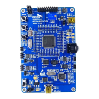
GD32E503V-EVAL Summary GD32E503V-EVAL uses GD32E503VET6 as the main controller. It uses GD-Link Mini USB interface to supply 5V power. Reset, Boot, K2, LED, I2S, I2C-EEPROM, LCD, NAND Flash, SPI-Flash, SDIO, USB and USART to USB interface are also included. For more details please refer to GD32E503V-EVAL-Rev1.0 schematic. - Page 8 User Guide GD32E503V-EVAL Function Description EXMC_D4 EXMC_D5 EXMC_D6 PE10 EXMC_D7 PD11 EXMC_A16 PD12 EXMC_A17 EXMC_NOE EXMC_NWE EXMC_NWAIT Nand_CS PD14 EXMC_D0 PD15 EXMC_D1 EXMC_D2 EXMC_D3 EXMC_D4 EXMC_D5 EXMC_D6 PE10 EXMC_D7 PE11 EXMC_D8 PE12 EXMC_D9 PE13 EXMC_D10 PE14 EXMC_D11 PE15 EXMC_D12 EXMC_D13...
-
Page 9: Getting Started
User Guide GD32E503V-EVAL Getting started The EVAL board uses GD-Link Mini USB connecter to get power DC +5V, which is the hardware system normal work voltage. A GD-Link on board is necessary in order to download and debug programs. Select the correct boot mode and then power on, the LEDPWR will turn on, which indicates the power supply is OK. -
Page 10: Key
User Guide GD32E503V-EVAL LED1 LED1 470Ω LED0603 LED2 LED2 470Ω LED0603 LED3 LED3 470Ω LED0603 LED4 LED4 470Ω LED0603 4.4. Figure 4-4. Schematic diagram of Key function +3V3 KEY_A KEY_Cet KEY_A 10KΩ 10KΩ 10KΩ 10KΩ 10KΩ KEY_B KEY_D PC13 KEY_B... -
Page 11: Usart
User Guide GD32E503V-EVAL 4.7. USART Figure 4-7. Schematic diagram of USART USART0 To USB +3V3 VBUS 50V/0.01uF RS232_TX RS232_RX PA10 RTS# +3V3 CTS# TNOW CH340E 50V/0.1uF Shield Mini_USB 1MΩ 50V/4700pF 4.8. Figure 4-8. Schematic diagram of I2C +3V3 50V/0.1uF 4.7KΩ... -
Page 12: Spi
User Guide GD32E503V-EVAL 4.10. Figure 4-10. Schematic diagram of SPI 4.11. NAND Figure 4-11. Schematic diagram of NAND Nand Flash +3V3 +3V3 EXMC_D7 VDD1 EXMC_D6 VDD2 EXMC_D5 50V/0.1uF 50V/0.1uF EXMC_D4 VSS1 EXMC_D3 VSS2 EXMC_D2 EXMC_D1 EXMC_D0 +3V3 R63 10KΩ EXMC_A16... -
Page 13: Lcd
User Guide GD32E503V-EVAL 4.12. Figure 4-12. Schematic diagram of LCD 4.13. SDIO Figure 4-13. Schematic diagram of SDIO SDIO +3V3 PC11 SDIO_DAT3 SDIO_CMD 10KΩ 10KΩ 10KΩ JP21 10KΩ PC12 SDIO_CLK SDIO_DAT0 SDIO_DAT1 +3V3 SDIO_DAT1 SDIO_DAT0 PC10 SDIO_DAT2 SDIO_CLK 16V/10uF,AVX +3V3... -
Page 14: Extension
User Guide GD32E503V-EVAL 4.15. Extension Figure 4-15. Schematic diagram of Extension Extension Pin JP10 JP11 PB12 PB13 PA14 PA15 PB14 PB15 PC10 PC11 VBAT PC12 PC13 PC14 PD10 PD11 PC15 PD12 PD13 PD14 PD15 +3.3V +3.3V +3.3V +3.3V OSC_IN OSC_OUT... -
Page 15: Mcu
User Guide GD32E503V-EVAL 4.17. Figure 4-17. Schematic diagram of MCU GDLink JTAG JNTRST PA0-WKUP L_TDI JTDI PA15 L_TMS/IO JTMS/SWDIO PA13 L_TCK/CLK JTCK/SWDCLK PA14 L_TDO/SWO JTDO L_TReset NRST +3V3 +3.3V VBAT PA10 PC10 PA10 PC10 +3V3 PA11 PC11 +3V3 PA11 PC11 表贴排阻... -
Page 16: Routine Use Guide
Learn to use SysTick to generate 1ms delay GD32E503V-EVAL-V1.0 board has five user keys and four LEDs. The keys are KEY_A, KEY_B, KEY_C, KEY_D and KEY_Cet. The LEDs are controlled by GPIO. This demo will show how to light the LEDs. -
Page 17: Exti_Key_Interrupt_Mode
Learn to use EXTI to generate external interrupt GD32E503V-EVAL-V1.0 board has five user keys and four LEDs. The keys are KEY_A, KEY_B, KEY_C, KEY_D, and KEY_Cet. The LEDs are controlled by GPIO. This demo will show how to use the EXTI interrupt line to control the LED2. When press down the KEY_B, it will produce an interrupt. -
Page 18: Usart_Hyperterminal_Interrupt
User Guide GD32E503V-EVAL 5.5. USART_HyperTerminal_Interrupt 5.5.1. DEMO purpose This demo includes the following functions of GD32 MCU: Learn to use the USART transmit and receive interrupts to communicate with the HyperTerminal. 5.5.2. DEMO running result Download the program <05_USART_HyperTerminal_Interrupt> to the EVAL board, connect serial cable to USART0. -
Page 19: Demo Running Result
Learn to get the value of inner channel 16(temperature sensor channel) and channel 17 (Vrefint channel) 5.7.2. DEMO running result Download the program <07_ADC_Temperature_Vrefint> to the GD32E503V-EVAL-V1.0 board. Connect serial cable to USART0, open the HyperTerminal. When the program is running, HyperTerminal display the value of temperature and internal voltage reference. -
Page 20: Adc0_Adc1_Follow_Up_Mode
Learn to use ADC0 and ADC1 follow-up mode 5.8.2. DEMO running result Download the program <08_ADC0_ADC1_Follow_up_mode> to the GD32E503V-EVAL-V1.0 board. Connect serial cable to USART0, open the HyperTerminal. PC3 and PC5 pin voltage access by external voltage. TIMER1_CH1 is the trigger source of ADC0 and ADC1. When the rising edge of TIMER1_CH1 coming, ADC0 starts immediately and ADC1 starts after a delay of several ADC clock cycles. -
Page 21: Adc0_Adc1_Regular_Parallel_Mode
User Guide GD32E503V-EVAL 5.9. ADC0_ADC1_Regular_Parallel_mode 5.9.1. DEMO purpose This demo includes the following functions of GD32 MCU: Learn to use the ADC to convert analog signal to digital data Learn to use ADC0 and ADC1 regular parallel mode 5.9.2. -
Page 22: Adc_Channel_Differential_Mode
Learn to use ADC channel differential mode 5.10.2. DEMO running result Download the program <10_ADC_Channel_Differential_mode > to the GD32E503V-EVAL- V1.0 board. Connect serial cable to USART0. Software is the trigger source of ADC0, and the continuous function is enabled. ADC0_IN12 (PC2) is configured in differential input mode. -
Page 23: Demo Running Result
User Guide GD32E503V-EVAL 5.11.2. DEMO running result Download the program <11_DAC_Output_Voltage_Value> to the EVAL board and run, all the LEDs will turn on and turn off for test. The DAC works in concurrent mode. The digital value of PA4 is 0x7FF0, its converted analog voltage should be 1.65V (VREF/2), and the digital value of PA5 is 0x1FF0, its converted... -
Page 24: Spi_Spi_Flash
User Guide GD32E503V-EVAL 5.13. SPI_SPI_Flash 5.13.1. DEMO purpose This demo includes the following functions of GD32 MCU: Learn to use the SPI unit to read and write NOR Flash with the SPI interface 5.13.2. DEMO running result The computer serial port line connected to the USART0 port of development board, set the baud rate of HyperTerminal software to 115200, 8 bits data bit, 1 bit stop bit. -
Page 25: I2S_Audio_Player
5.15.2. DEMO running result GD32E503V-EVAL board has EXMC module to control NAND flash. Before running the demo, P2 and P3 must be fitted to the EXMC port, JP24 must be fitted to the Nand port. Download the program <15_EXMC_NandFlash> to the EVAL board. This demo shows the write and read operation process of NAND flash memory by EXMC module. -
Page 26: Exmc_Touchscreen
5.16.2. DEMO running result GD32E503V-EVAL board has EXMC module to control LCD. Before running the demo, JP12 must be fitted to the SPI0 port, P2 and P3 must be fitted to the EXMC port, JP24 must be fitted to the Lcd port. Download the program <16_EXMC_TouchScreen> to the EVAL board. -
Page 27: Sdio_Sdcardtest
Learn to use SDIO to erase, lock and unlock a SD card GD32E503V-EVAL board has a secure digital input/output interface (SDIO) which defines the SD/SD I/O /MMC CE-ATA card host interface. This demo will show how to use SDIO to operate on SD card. -
Page 28: Rcu_Clock_Out
User Guide GD32E503V-EVAL LED2, LED4. Otherwise, turn on all the LEDs. Uncomment the macro DATA_PRINT to print out the data and display them through HyperTerminal. Set bus mode(1-bit or 4-bit) and data transfer mode(polling mode or DMA mode) by comment and uncomment the related statements. -
Page 29: Ctc_Calibration
User Guide GD32E503V-EVAL 5.19. CTC_Calibration 5.19.1. DEMO purpose This demo includes the following functions of GD32 MCU: Learn to use external low speed crystal oscillator (LXTAL) to implement the CTC calibration function Learn to use clock trim controller (CTC) to trim internal 48MHz RC oscillator (IRC48M) -
Page 30: Demo Running Result
User Guide GD32E503V-EVAL Learn to use RTC module to implement calendar function Learn to use USART module to implement time display 5.21.2. DEMO running result Download the program <21_RTC_Calender> to the EVAL board and run. Connect serial cable to USART0, open the HyperTerminal. After start-up, the program will ask to set the time on the HyperTerminal. -
Page 31: Usbd_Keyboard
Learn how to implement USB HID(human interface) device The GD32E503V-EVAL board is enumerated as an USB Keyboard, which uses the native PC Host HID driver, as shown below. The USB Keyboard uses Joystick to output three characters (‘b’, ‘a’ and ‘c’). In addition, the demo also supports remote wakeup which is the ability of a USB device to bring a suspended bus back to the active condition, and the ‘a’... -
Page 32: Demo Running Result
User Guide GD32E503V-EVAL Learn how to implement USB CDC device GD32E503V-EVAL board has one USBD interface. In this demo, the GD32E503V-EVAL board is enumerated as an USB virtual COM port, which was shown in device manager of PC as below. This demo makes the USB device look like a serial port, and loops back the contents of a text file over USB port. -
Page 33: Revision History
User Guide GD32E503V-EVAL Revision history Table 6-1. Revision history Revision No. Description Date Initial Release Sep.4, 2020 32/33... - Page 34 Important Notice This document is the property of GigaDevice Semiconductor Inc. and its subsidiaries (the "Company"). This document, including any product of the Company described in this document (the “Product”), is owned by the Company under the intellectual property laws and treaties of the People’s Republic of China and other jurisdictions worldwide.
Need help?
Do you have a question about the GD32E503V-EVAL and is the answer not in the manual?
Questions and answers