Table of Contents
Advertisement
Quick Links
Advertisement
Table of Contents

Related Manuals for GigaDevice Semiconductor GD32E503Z-EVAL


Summary of Contents for GigaDevice Semiconductor GD32E503Z-EVAL
- Page 1 GigaDevice Semiconductor Inc. GD32E503Z-EVAL User Guide V1.2...
-
Page 2: Table Of Contents
User Guide GD32E503Z-EVAL Tables of Contents TABLES OF CONTENTS ....................1 LIST OF FIGURES ......................4 LIST OF TABLES ......................5 1. SUMMARY ........................ 6 2. FUNCTION PIN ASSIGN ................... 6 3. GETTING STARTED ....................8 4. HARDWARE LAYOUT OVERVIEW ................8 4.1. - Page 3 User Guide GD32E503Z-EVAL 5.4.2. DEMO running result ......................16 5.5. USART_HyperTerminal_Interrupt ................17 5.5.1. DEMO purpose ........................17 5.5.2. DEMO running result ......................17 5.6. USART_DMA ......................17 5.6.1. DEMO purpose ........................17 5.6.2. DEMO running result ......................17 5.7.
- Page 4 User Guide GD32E503Z-EVAL 5.19.1. DEMO purpose ........................28 5.19.2. DEMO running result ......................28 5.20. CTC_Calibration ..................... 28 5.20.1. DEMO purpose ........................28 5.20.2. DEMO running result ......................29 5.21. PMU_Sleep_Wakeup ....................29 5.21.1. DEMO purpose ........................29 5.21.2. DEMO running result ......................29 5.22.
-
Page 5: List Of Figures
User Guide GD32E503Z-EVAL List of Figures Figure 4-1. Schematic diagram of power supply ..................8 Figure 4-2. Schematic diagram of boot option ..................8 Figure 4-3. Schematic diagram of LED function ..................9 Figure 4-4. Schematic diagram of Key function ..................9 Figure 4-5. -
Page 6: List Of Tables
User Guide GD32E503Z-EVAL List of Tables Table 2-1. Function pin assignment ......................6 Table 6-1. Revision history ........................32 5/33... -
Page 7: Summary
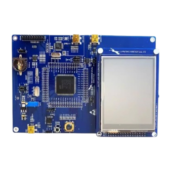
GD32E503Z-EVAL Summary GD32E503Z-EVAL uses GD32E503ZET6 as the main controller. It uses GD-Link Mini USB interface to supply 5V power. Reset, Boot, K2, LED, I2S, I2C-EEPROM, LCD, NAND Flash, SPI-Flash, SDIO, USB and USART to USB interface are also included. For more details please refer to GD32E503Z-EVAL-Rev1.0 schematic. - Page 8 User Guide GD32E503Z-EVAL Function Description EXMC_D3 EXMC_D4 EXMC_D5 EXMC_D6 PE10 EXMC_D7 PD11 EXMC_A16 PD12 EXMC_A17 EXMC_NOE EXMC_NWE EXMC_NWAIT EXMC_NCE1 PD14 EXMC_D0 PD15 EXMC_D1 EXMC_D2 EXMC_D3 EXMC_D4 EXMC_D5 EXMC_D6 PE10 EXMC_D7 PE11 EXMC_D8 PE12 EXMC_D9 PE13 EXMC_D10 PE14 EXMC_D11 PE15 EXMC_D12...
-
Page 9: Getting Started
User Guide GD32E503Z-EVAL Getting started The EVAL board uses GD-Link Mini USB connecter to get power DC +5V, which is the hardware system normal work voltage. A GD-Link on board is necessary in order to download and debug programs. Select the correct boot mode and then power on, the LEDPWR will turn on, which indicates the power supply is OK. -
Page 10: Led
User Guide GD32E503Z-EVAL 4.3. Figure 4-3. Schematic diagram of LED function LED1 LED1 470Ω LED0603 LED2 LED2 470Ω LED0603 LED3 LED3 470Ω LED0603 LED4 LED4 470Ω LED0603 4.4. Figure 4-4. Schematic diagram of Key function +3V3 10KΩ 10KΩ 10KΩ 10KΩ... -
Page 11: Can
User Guide GD32E503Z-EVAL PA5 is an AFIO, please refer to SPI Schematic for right config DAC_OUT1 DAC_OUT0 4.7. Figure 4-7. Schematic diagram of CAN 4.8. USART Figure 4-8. Schematic diagram of USART 4.9. Figure 4-9. Schematic diagram of I2C +3V3 50V/0.1uF... -
Page 12: I2S
User Guide GD32E503Z-EVAL 4.10. Figure 4-10. Schematic diagram of I2S 10KΩ I2S_MCK I2S_SD +3V3 C31 50V/0.1uF SDIN AOUTR PB12 I2S_WS I2S_CK SCLK 470Ω PB13 I2S_CK I2S_WS 16V/3.3uF,AVX LRCK PB15 I2S_SD I2S_MCK MCLK AOUTL FILT+ 470Ω HeadPhone 10KΩ CS4344 16V/3.3uF,AVX 50V/0.1uF... -
Page 13: Lcd
User Guide GD32E503Z-EVAL 4.13. Figure 4-13. Schematic diagram of LCD 4.14. SDIO Figure 4-14. Schematic diagram of SDIO +3V3 SDIO +3V3 10KΩ 10KΩ 10KΩ SDIO_CMD 10KΩ JP21 PC12 SDIO_CLK SDIO_DAT0 SDIO_DAT1 16V/10uF,AVX SDIO_DAT1 SDIO_DAT0 PC10 SDIO_DAT2 PC11 SDIO_DAT3 SDIO_CLK +3V3... -
Page 14: Extension
User Guide GD32E503Z-EVAL 4.16. Extension Figure 4-16. Schematic diagram of Extension 4.17. GD-Link Figure 4-17. Schematic diagram of GD-Link +3V3 JP100 PA0-WKUP L_SWDIO L_SWDCK PB2/BOOT1 PB3/JTDO L_TMS/IO PB4/JNTRST 4× 1P2.54 L_TCK/CLK L_TDO/SWO L_TDI L_USB_Ctr L_TReset L_LED1 LED0603 PA10 PB10 C100... -
Page 15: Mcu
User Guide GD32E503Z-EVAL 4.18. Figure 4-18. Schematic diagram of MCU +3.3V +3.3V +3.3V +3.3V +3.3V +3.3V GD32E503ZET6 PG10 PG10 PG11 PG11 PG12 PG12 PG13 PG13 PA10 PG14 PA10 PG14 PA11 PG15 PA11 PG15 PA12 PA12 PA13 PA13/JTMS-SWDIO PA14 PA14/JTCK-SWCLK PA15... -
Page 16: Routine Use Guide
Learn to use SysTick to generate 1ms delay GD32E503Z-EVAL-V1.0 board has five user keys and four LEDs. The keys are KEY_A, KEY_B, KEY_C, KEY_D and KEY_Cet. The LEDs are controlled by GPIO. This demo will show how to light the LEDs. -
Page 17: Exti_Key_Interrupt_Mode
Learn to use EXTI to generate external interrupt GD32E503Z-EVAL-V1.0 board has five user keys and four LEDs. The keys are KEY_A, KEY_B, KEY_C, KEY_D, and KEY_Cet. The LEDs are controlled by GPIO. This demo will show how to use the EXTI interrupt line to control the LED2. When press down the KEY_B, it will produce an interrupt. -
Page 18: Usart_Hyperterminal_Interrupt
User Guide GD32E503Z-EVAL 5.5. USART_HyperTerminal_Interrupt 5.5.1. DEMO purpose This demo includes the following functions of GD32 MCU: Learn to use the USART transmit and receive interrupts to communicate with the HyperTerminal. 5.5.2. DEMO running result Download the program <05_USART_HyperTerminal_Interrupt> to the EVAL board, connect serial cable to USART0. -
Page 19: Adc_Temperature_Vrefint
Learn to get the value of inner channel 16(temperature sensor channel) and channel 17 (Vrefint channel) 5.7.2. DEMO running result Download the program <07_ADC_Temperature_Vrefint> to the GD32E503Z-EVAL-V1.0 board. Connect serial cable to USART0, open the HyperTerminal. When the program is running, HyperTerminal display the value of temperature and internal voltage reference. -
Page 20: Adc0_Adc1_Follow_Up_Mode
Learn to use ADC0 and ADC1 follow-up mode 5.8.2. DEMO running result Download the program <08_ADC0_ADC1_Follow_up_mode> to the GD32E503Z-EVAL-V1.0 board. Connect serial cable to USART0, open the HyperTerminal. PC3 and PC5 pin voltage access by external voltage. TIMER1_CH1 is the trigger source of ADC0 and ADC1. When the rising edge of TIMER1_CH1 coming, ADC0 starts immediately and ADC1 starts after a delay of several ADC clock cycles. -
Page 21: Adc0_Adc1_Regular_Parallel_Mode
User Guide GD32E503Z-EVAL 5.9. ADC0_ADC1_Regular_Parallel_mode 5.9.1. DEMO purpose This demo includes the following functions of GD32 MCU: Learn to use the ADC to convert analog signal to digital data Learn to use ADC0 and ADC1 regular parallel mode 5.9.2. -
Page 22: Adc_Channel_Differential_Mode
Learn to use ADC channel differential mode 5.10.2. DEMO running result Download the program <10_ADC_Channel_Differential_mode > to the GD32E503Z-EVAL- V1.0 board. Connect serial cable to USART0. Software is the trigger source of ADC0, and the continuous function is enabled. ADC0_IN12 (PC2) is configured in differential input mode. -
Page 23: Demo Running Result
User Guide GD32E503Z-EVAL 5.11.2. DEMO running result Download the program <11_DAC_Output_Voltage_Value> to the EVAL board and run, all the LEDs will turn on and turn off for test. The DAC works in concurrent mode. The digital value of PA4 is 0x7FF0, its converted analog voltage should be 1.65V (VREF/2), and the digital value of PA5 is 0x1FF0, its converted... -
Page 24: Spi_Spi_Flash
User Guide GD32E503Z-EVAL 5.13. SPI_SPI_Flash 5.13.1. DEMO purpose This demo includes the following functions of GD32 MCU: Learn to use the SPI unit to read and write NOR Flash with the SPI interface 5.13.2. DEMO running result The computer serial port line connected to the USART0 port of development board, set the baud rate of HyperTerminal software to 115200, 8 bits data bit, 1 bit stop bit. -
Page 25: I2S_Audio_Player
5.15.2. DEMO running result GD32E503Z-EVAL board has EXMC module to control NAND flash. Before running the demo, JP13 must be fitted to USART0, P2 and P3 must be fitted to the EXMC port, JP22 must be fitted to the Nwait port. Download the program <15_EXMC_NandFlash> to the EVAL board. -
Page 26: Exmc_Touchscreen
5.16.2. DEMO running result GD32E503Z-EVAL board has EXMC module to control LCD. Before running the demo, JP12 must be fitted to the SPI0 port, P2 and P3 must be fitted to the EXMC port. Download the program <16_EXMC_TouchScreen> to the EVAL board. This demo displays GigaDevice logo and four green buttons on the LCD screen by EXMC module. -
Page 27: Sdio_Sdcardtest
Learn to use SDIO to erase, lock and unlock a SD card GD32E503Z-EVAL board has a secure digital input/output interface (SDIO) which defines the SD/SD I/O /MMC CE-ATA card host interface. This demo will show how to use SDIO to operate on SD card. -
Page 28: Can
User Guide GD32E503Z-EVAL LED2, LED4. Otherwise, turn on all the LEDs. Uncomment the macro DATA_PRINT to print out the data and display them through HyperTerminal. Set bus mode(1-bit or 4-bit) and data transfer mode(polling mode or DMA mode) by comment and uncomment the related statements. -
Page 29: Rcu_Clock_Out
User Guide GD32E503Z-EVAL 5.19. RCU_Clock_Out 5.19.1. DEMO purpose This demo includes the following functions of GD32 MCU: Learn to use GPIO control the LED Learn to use the clock output function of RCU Learn to communicate with PC by USART 5.19.2. -
Page 30: Demo Running Result
User Guide GD32E503Z-EVAL 5.20.2. DEMO running result Download the program <20_CTC_Calibration> to the EVAL board and run. If the clock trim is OK, LED2 will be on. Otherwise, LED2 will be turned off. 5.21. PMU_Sleep_Wakeup 5.21.1. DEMO purpose This Demo includes the following functions of GD32 MCU: ... -
Page 31: Shrtimer_Timer_Breath_Led
Learn how to implement USB HID(human interface) device The GD32E503Z-EVAL board is enumerated as an USB Keyboard, which uses the native PC Host HID driver, as shown below. The USB Keyboard uses Joystick to output three characters (‘b’, ‘a’ and ‘c’). In addition, the demo also supports remote wakeup which is the ability of a... -
Page 32: Demo Running Result
User Guide GD32E503Z-EVAL USB device to bring a suspended bus back to the active condition, and the ‘a’ key is used as the remote wakeup source. 5.24.2. DEMO Running Result Download the program <24_USBD_Keyboard> to the EVAL board and run. If you press the A key, will output ‘a’. -
Page 33: Revision History
User Guide GD32E503Z-EVAL Revision history Table 6-1. Revision history Revision No. Description Date Initial Release Jun.30, 2020 Module update Aug.26, 2020 Add CAN Mar.31, 2021 32/33... - Page 34 Important Notice This document is the property of GigaDevice Semiconductor Inc. and its subsidiaries (the "Company"). This document, including any product of the Company described in this document (the “Product”), is owned by the Company under the intellectual property laws and treaties of the People’s Republic of China and other jurisdictions worldwide.
Need help?
Do you have a question about the GD32E503Z-EVAL and is the answer not in the manual?
Questions and answers