Table of Contents
Advertisement
Quick Links
SERVICE MANUAL
Ver. 1.0 2013.03
• HCD-GPX33 is the amplifi er, USB, CD player,
Bluetooth, NFC and tuner section in MHC-GPX33.
• HCD-GPX55 is the amplifi er, USB, CD player,
Bluetooth, NFC and tuner section in MHC-GPX55.
• HCD-GPX77 is the amplifi er, USB, CD player,
Bluetooth, NFC and tuner section in MHC-GPX77.
• HCD-GPX88 is the amplifi er, USB, CD player,
Bluetooth, NFC and tuner section in MHC-GPX88.
"WALKMAN" and "WALKMAN" logo are registered trademarks of Sony Corporation.
MPEG Layer-3 audio coding technology and patents licensed from Fraunhofer IIS and Thomson.
Windows Media is either a registered trademark or trademark of Microsoft Corporation in the United States
and/or other countries.
This product is protected by certain intellectual property rights of Microsoft Corporation. Use or distribution
of such technology outside of this product is prohibited without a license from Microsoft or an authorized
Microsoft subsidiary.
The Bluetooth
®
word mark and logos are registered trademarks owned by Bluetooth SIG, Inc. and any use
of such marks by Sony Corporation is under license. Other trademarks and trade names are those of their
respective owners.
The N Mark is a trademark or registered trademark of NFC Forum, Inc. in the United States and in other
countries.
Android is a trademark of Google Inc.
All other trademarks and registered trademarks are of their respective holders. In this manual, ™ and ® marks
are not specified.
AUDIO POWER SPECIFICATIONS
POWER OUTPUT AND TOTAL HARMONIC
DISTORTION:
(USA model only)
With 4 ohm loads, both channels driven, from
120 – 10,000 Hz; rated 130 watts per channel
minimum RMS power, with no more than
0.7% total harmonic distortion from 250
milliwatts to rated output.
Amplifi er section
The following are measured at
USA model:
AC 120 V, 60 Hz
Mexican model:
AC 120 V – 240 V, 60 Hz
Other models:
AC 120 V – 240 V, 50/60 Hz
MHC-GPX88
Front speaker
Power Output (rated):
350 W + 350 W (at 4 ohms, 1 kHz,
1% THD)
RMS output power (reference):
600 W + 600 W (per channel at 4 ohms,
1 kHz)
Subwoofer
RMS output power (reference):
500 W + 500 W (per channel at 5 ohms,
100 Hz)
LBT-GPX77/MHC-GPX77
HIGH speakers
Power Output (rated):
350 W + 350 W (at 4 ohms, 1 kHz,
1% THD)
RMS output power (reference):
600 W + 600 W (per channel at 4 ohms,
1 kHz)
LOW speakers
RMS output power (reference):
300 W + 300 W (8 ohms, 100 Hz)
9-890-622-01
Sony Corporation
2013C80-1
©
2013.03
Published by Sony EMCS (Malaysia) PG Tec
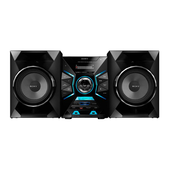
HCD-GPX33/GPX55/GPX77/
Photo: HCD-GPX88
SPECIFICATIONS
LBT-GPX55/MHC-GPX55
Front speaker
Power Output (rated):
350 W + 350 W (at 4 ohms, 1 kHz,
1% THD)
RMS output power (reference):
550 W + 550 W (per channel at 4 ohms,
1 kHz)
Subwoofer
RMS output power (reference):
500 W (5 ohms, 100 Hz)
MHC-GPX33
Front speaker
Power Output (rated):
350 W + 350 W (at 4 ohms, 1 kHz,
1% THD)
RMS output power (reference):
600 W + 600 W (per channel at
4 ohms, 1 kHz)
Inputs
TV/DVD/SAT (AUDIO IN) L/R
Voltage 2 V, impedance 47 kilohms
PC/GAME (AUDIO IN) L/R
Voltage 2 V, impedance 47 kilohms
MIC (MHC-GPX88 only)
Sensitivity 1 mV, impedance 10 kilohms
A (USB),
B (USB) port: Type A
USB section
Supported bit rate
WMA:
48 kbps – 192 kbps, VBR, CBR
AAC:
48 kbps – 320 kbps, VBR, CBR
Sampling frequencies
WMA: 44.1 kHz
AAC: 44.1 kHz
Supported USB device
Mass Storage Class
Maximum current
500 mA
HCD-GPX33/GPX55/GPX77/GPX88
Saudi Arabia Model
Model Name Using
Similar Mechanism
CD Section
CD Mechanism Type
Optical Pick-up Name
Disc/USB section
Supported bit rate
MPEG1 Layer-3:
32 kbps – 320 kbps, VBR
MPEG2 Layer-3:
8 kbps – 160 kbps, VBR
MPEG1 Layer-2:
32 kbps – 384 kbps, VBR
Sampling frequencies
MPEG1 Layer-3:
32 kHz/44.1 kHz/48 kHz
MPEG2 Layer-3:
16 kHz/22.05 kHz/24 kHz
MPEG1 Layer-2:
32 kHz/44.1 kHz/48 kHz
Disc player section
System
Compact disc and digital audio system
Laser Diode Properties
Emission Duration: Continuous
Laser Output*: Less than 44.6 W
* This output is the value measurement
at a distance of 200 mm from the
objective lens surface on the Optical
Pick-up Block with 7 mm aperture.
Frequency response
20 Hz – 20 kHz
Signal-to-noise ratio
More than 90 dB
Dynamic range
More than 88 dB
Tuner section
FM stereo, FM/AM superheterodyne tuner
Antenna:
FM lead antenna
AM loop antenna
FM tuner section
Tuning range
USA and Brazilian models:
87.5 MHz – 108.0 MHz
(100 kHz step)
Other models:
87.5 MHz – 108.0 MHz (50 kHz step)
COMPACT DISC RECEIVER
GPX88
US Model
HCD-GPX55/GPX77
E Model
Australian Model
HCD-GPX77
Mexican Model
HCD-GPX33/GPX77/GPX88
HCD-GPX33/GPX77
NEW
CDM90-DVBU202//M
CMS-S76RFS7G
AM tuner section
Tuning range
Pan American and Australia models:
531 kHz – 1,710 kHz (9 kHz step)
530 kHz – 1,710 kHz (10 kHz step)
Saudi Arabian model:
531 kHz – 1,602 kHz (9 kHz step)
Other models:
531 kHz – 1,602 kHz (9 kHz step)
530 kHz – 1,610 kHz (10 kHz step)
Bluetooth section
Communication system
Bluetooth Standard version 3.0 +
EDR (Enhanced Date Rate)
Output
Bluetooth Standard Power Class 2
Maximum communication range
Line of sight approx. 10 m
1)
Frequency band
2.4 GHz band (2.4000 GHz – 2.4835 GHz)
Modulation method
FHSS (Freq Hopping Spread Spectrum)
Compatible Bluetooth profiles
2)
A2DP (Advanced Audio Distribution
Profile)
AVRCP 1.3 (Audio Video Remote
Control Profile)
Supported codecs
SBC (Sub Band Codec)
AAC (Advanced Audio Coding)
1)
The actual range will vary depending on
factors such as obstacles between devices,
magnetic fields around a microwave oven,
static electricity, reception sensitivity,
antenna's performance, operating system,
software application, etc.
Bluetooth standard profiles indicate the
2)
purpose
of
Bluetooth
communication
between devices.
– Continued on next page –
Advertisement
Table of Contents

Related Manuals for Sony HCD-GPX33


Summary of Contents for Sony HCD-GPX33
- Page 1 ® word mark and logos are registered trademarks owned by Bluetooth SIG, Inc. and any use of such marks by Sony Corporation is under license. Other trademarks and trade names are those of their respective owners. The N Mark is a trademark or registered trademark of NFC Forum, Inc. in the United States and in other countries.
- Page 2 COMPONENTS IDENTIFIED BY MARK 0 OR DOTTED LINE WITH MARK 0 ON THE SCHEMATIC DIAGRAMS AND IN THE PARTS LIST ARE CRITICAL TO SAFE OPERATION. REPLACE THESE COMPONENTS WITH SONY PARTS WHOSE PART NUMBERS APPEAR AS SHOWN IN THIS MANUAL OR IN SUPPLEMENTS PUBLISHED BY SONY.
-
Page 3: Table Of Contents
HCD-GPX33/GPX55/GPX77/GPX88 TABLE OF CONTENTS SERVICING NOTES 6-20. Printed Wiring Board - MIC Board (GPX88) - ..... 43 ..........6-21. Schematic Diagram - MIC Board (GPX88) - ....43 DISASSEMBLY 6-22. Printed Wiring Board - VOLUME Board - ..... 44 6-23. Schematic Diagram - VOLUME Board - ....... 44 2-1. -
Page 4: Servicing Notes
HCD-GPX33/GPX55/GPX77/GPX88 SECTION 1 SERVICING NOTES MODEL IDENTIFICATION NOTES ON HANDLING THE OPTICAL PICK-UP – Back Panel – BLOCK OR BASE UNIT The laser diode in the optical pick-up block may suffer electro- static break-down because of the potential difference generated by the charged electrostatic load, etc. - Page 5 HCD-GPX33/GPX55/GPX77/GPX88 HOW TO OPEN THE TRAY WHEN POWER SWITCH TURN OFF Note 1: After the side panel (L, R) and top panel is removed, this work is done. Note 2: Please prepare the thin wire (clip etc. processed to the length of 8 cm or more).
- Page 6 HCD-GPX33/GPX55/GPX77/GPX88 CAPACITOR DISCHARGE FOR ELECTRIC SHOCK PREVENTION in checking the MB board, make a capacitor discharge of C1183 or C1020 or C1185 and C1021 for electrical shock prevention. C1021 C1185 C1020 C1183 MB board in checking the REGULATOR, SWITCHING board, make a capacitor discharge of C531 for electrical shock prevention.
- Page 7 – you may have to press N twice. Bluetooth device. – you may need to start playback of an audio source on the For example, select “SONY MHC-GPX88” (or LBT-GPX77/ Bluetooth device. GPX55/MHC-GPX77/GPX55/ GPX33). If passkey is required on the Bluetooth device, enter “0000”.
-
Page 8: Disassembly
HCD-GPX33/GPX55/GPX77/GPX88 SECTION 2 DISASSEMBLY • This set can be disassembled in the order shown below. 2-1. DISASSEMBLY FLOW 2-2. SIDE-L PANEL, SIDE-R PANEL, TOP PANEL (Page 9) 2-3. LOADING PANEL 2-4. FRONT PANEL SECTION 2-5. CD MECHANISM SECTION (Page 9) -
Page 9: Side-L Panel, Side-R Panel, Top Panel
HCD-GPX33/GPX55/GPX77/GPX88 Note: Follow the disassembly procedure in the numerical order given. 2-2. SIDE-L PANEL, SIDE-R PANEL, TOP PANEL 2 two screws (+BVTP 3 4 panel, side-L 0 panel, top 6 two screws (+BVTP 3 1 two screws (+BVTP 3 8 panel, side-R... -
Page 10: Front Panel Section
HCD-GPX33/GPX55/GPX77/GPX88 2-4. FRONT PANEL SECTION 6 flexible flat cable (14 core) (CN180) 5 wire (flat type) 3 one screw (8 core) (CN1507) (+BVTP 3 (GPX88) 0 front panel section 8 CN150 (4P) 4 one screw (+BVTP 3 7 wire (flat type) -
Page 11: Mb Board
HCD-GPX33/GPX55/GPX77/GPX88 2-6. MB BOARD (GPX33) (GPX55/GPX77/GPX88) 7 clamp, lead qd two screws qd three screws 8 panel, back (+PTPWH 2.6 (+PTPWH 2.6 (DIA8.0)) (DIA8.0)) 2 five screws qg heat sink (+BVTP 3 qg heat sink (GSX3) (GSX8) 5 bushing (FBS001), cord... -
Page 12: Service Optical Device, Wire (Flat Type)
HCD-GPX33/GPX55/GPX77/GPX88 2-8. SERVICE OPTICAL DEVICE, WIRE (FLAT TYPE) Note 1 : Before disconnecting the fl exible fl at cable (24 core) of optical pick-up block, solder the short-land. 2 chuck holder assy (T) 2 Solder the short-land. 1 six claws... -
Page 13: Test Mode
HCD-GPX33/GPX55/GPX77/GPX88 SECTION 3 TEST MODE [PANEL TEST MODE] [MODEL & DEST WRITE MODE] This mode is used to set software model & destination. This mode is used to check the fl uorescent indicator tube, LEDs, This mode is only available when no permanent model & destina- keys, [MASTER VOLUME / DJ CONTROL] jog, model, destina- tion is stored. - Page 14 HCD-GPX33/GPX55/GPX77/GPX88 [USER RESET] [CDM AGING MODE] The user reset clears all data including preset data stored in the data This mode is used for CDM aging. fl ash to initial conditions exclude history mode data. Procedure: 1. Press [ / STANDBY] button to turn on the system.
- Page 15 HCD-GPX33/GPX55/GPX77/GPX88 Display Item Protector Count ※ ※ Protector Type (refer PROTECTOR KIND CHECK TEST MODE) Protector type Protector Error Code AMPL PWR2 ※ ※ ※ ※ TEMP Single Power On Time ※ ※ ※ ※ ※ ※ ※ M Total Power On Time ※...
-
Page 16: Electrical Check
HCD-GPX33/GPX55/GPX77/GPX88 SECTION 4 ELECTRICAL CHECK CD SECTION 0 dB = 1 μV TUNER SECTION FM AUTO STOP CHECK Note: 1. CD Block is basically constructed to operate without adjustment. signal 2. Use YEDS-18 disc (Part No. 3-702-101-01) unless otherwise indicat- generator 3. -
Page 17: Troubleshooting
HCD-GPX33/GPX55/GPX77/GPX88 SECTION 5 TROUBLESHOOTING... - Page 18 HCD-GPX33/GPX55/GPX77/GPX88...
- Page 19 HCD-GPX33/GPX55/GPX77/GPX88...
- Page 20 HCD-GPX33/GPX55/GPX77/GPX88...
- Page 21 HCD-GPX33/GPX55/GPX77/GPX88...
- Page 22 HCD-GPX33/GPX55/GPX77/GPX88...
-
Page 23: Diagrams
HCD-GPX33/GPX55/GPX77/GPX88 SECTION 6 DIAGRAMS 6-1. BLOCK DIAGRAM - CD/USB Section - GPX55/GPX77/GPX88 STEREO A/D CONVERTER IC765 MAIN L-OUT VOUTL SECTION (Page 24) VOUTR R-CH LRCK DATA STEREO A/D CONVERTER AUDIO DSP IC750 IC701 ASYNCHRONOUS SAMPLE MAIN SIGNAL SELECTOR RATE CONVERTER... -
Page 24: Block Diagram - Main Section
HCD-GPX33/GPX55/GPX77/GPX88 6-2. BLOCK DIAGRAM - MAIN Section - GPX55/GPX77/GPX88 OP AMP IC951 CD/USB L-OUT SW OUT L SECTION SECTION (Page 25) (Page 23) OP AMP IC950 CD/USB L-OUT FRONT-L SECTION SECTION (Page 23) (Page 25) MAIN SIGNAL SELECTOR L-CH IC1600... -
Page 25: Block Diagram - Amp Section
HCD-GPX33/GPX55/GPX77/GPX88 6-3. BLOCK DIAGRAM - AMP Section - GPX88 POWER AMP GPX77/GPX88 GPX55 IC1004 POWER AUDIO DRIVER TB1000 Q1015 SW OUT L GPX55/ OR AMP SD SWITCH POWER AUDIO MAIN GPX77/GPX88 IC1001 DRIVER Q1005 SECTION Q1018 (Page 24) RESET SWITCH... -
Page 26: Block Diagram - Panel/Power Supply Section
HCD-GPX33/GPX55/GPX77/GPX88 6-4. BLOCK DIAGRAM - PANEL/POWER SUPPLY Section - +13V SEL A : DISPLAY BOARD D1008, D1009, D1012, D1013, D1016, D1017, D1018, D1019, D1023, D1027 DYNAMIC LED VACUUM LED +5.2V DRIVING FLUORESCENT Q2100 - Q2103 DISPLAY SEL B: FL2200 DISPLAY BOARD... - Page 27 HCD-GPX33/GPX55/GPX77/GPX88 THIS NOTE IS COMMON FOR PRINTED WIRING BOARDS AND SCHEMATIC DIAGRAMS. • Circuit Boards Location (In addition to this, the necessary note is printed in each block.) For Printed Wiring Boards. For Schematic Diagrams. Note: Note: • X : Parts extracted from the component side.
-
Page 28: Mb Board (Component Side)
HCD-GPX33/GPX55/GPX77/GPX88 6-5. PRINTED WIRING BOARD - MB Board (Component Side) - • See page 27 for Circuit Boards Location. • : Uses unleaded solder. MB BOARD GPX55 TB1002 (COMPONENT SIDE) SUBWOOFERS IMPEDANCE GPX77/GPX88 TB1000 SUBWOOFERS IMPEDANCE TB1001 J1600 FRONT SPEAKERS... -
Page 29: Printed Wiring Board - Mb Board (Conductor Side)
HCD-GPX33/GPX55/GPX77/GPX88 6-6. PRINTED WIRING BOARD - MB Board (Conductor Side) - • See page 27 for Circuit Boards Location. • : Uses unleaded solder. MB BOARD (CONDUCTOR SIDE) LED SPEAKERS GPX88 GPX77/GPX88 CN1502 CN1505 FRONT SUBWOOFERS SPEAKERS GPX55/GPX77/ GPX88 JL118... -
Page 30: Schematic Diagram - Mb Board (1/9)
HCD-GPX33/GPX55/GPX77/GPX88 6-7. SCHEMATIC DIAGRAM - MB Board (1/9) - • See page 45 for Waveforms. • See page 46 for IC Block Diagrams. MB BOARD (1/9) MB BOARD (3/9) TAS-RESET DVDD3.3V (Page 32) R949 TAS-INT FE_3.3V_1 TAS-MUTE MB BOARD JL940 DMB-DVDD+3.3V... -
Page 31: Schematic Diagram - Mb Board (2/9)
HCD-GPX33/GPX55/GPX77/GPX88 6-8. SCHEMATIC DIAGRAM - MB Board (2/9) - • See page 45 for Waveforms. • See page 46 for IC Block Diagrams. • See page 52 for IC Pin Function Descriptions. MB BOARD (1/9) MB BOARD (3/9) (Page 30) -
Page 32: Schematic Diagram - Mb Board (3/9)
HCD-GPX33/GPX55/GPX77/GPX88 6-9. SCHEMATIC DIAGRAM - MB Board (3/9) - • See page 46 for IC Block Diagrams. MB BOARD (3/9) FE_DVD_LDD FB846 FE_DVD_IOP CL840 FE_3.3V_1 MB BOARD (1/9) MB BOARD (Page 30) R881 DVDD3.3V (2/9) (Page 31) R884 MB BOARD (2/9) -
Page 33: Schematic Diagram - Mb Board (4/9)
HCD-GPX33/GPX55/GPX77/GPX88 6-10. SCHEMATIC DIAGRAM - MB Board (4/9) - • See page 46 for IC Block Diagrams. R1018 MB BOARD (4/9) C1050 C1054 4.7k (GPX55/GPX77) R1018 R1034 10 16V 5.6k (GPX88) C1011 47 16V R1029 C1061 GPX55/ R1001 GPX77/ 4.7k... -
Page 34: Schematic Diagram - Mb Board (5/9)
C1174 R1239 IRF6775MTR1PBF C1107 C1136 D1011, D1012 470p GPX77/GPX88 2.2k POWER AUDIO C1183 C1303 0.001 1000p R1199 R1333 CRH02 (T5R, SONY, XM) JL1056 D1011 DRIVER 3300 71V 220p 4.7k TB1000 -2.6 JL1046 1 VAA C1294 R1200 R1205 R1206 D1012 61.3... -
Page 35: Schematic Diagram - Mb Board (6/9)
HCD-GPX33/GPX55/GPX77/GPX88 6-12. SCHEMATIC DIAGRAM - MB Board (6/9) - MB BOARD (4/9) MB BOARD (5/9) (Page 33) (Page 34) 31 32 33 34 MB BOARD (6/9) R1370 2.7k Q1051 LSCR523UBFS8TL R1434 PROTECTION R1371 SWITCH 2.7k /THERMISTER /AMP-RESET R1433 BOARD /AMP-OCP... -
Page 36: Schematic Diagram - Mb Board (7/9)
HCD-GPX33/GPX55/GPX77/GPX88 6-13. SCHEMATIC DIAGRAM - MB Board (7/9) - • See page 45 for Waveforms. • See page 46 for IC Block Diagrams. • See page 52 for IC Pin Function Descriptions. MB BOARD (7/9) L464 MB BOARD (9/9) 2.2nH... -
Page 37: Schematic Diagram - Mb Board (8/9)
HCD-GPX33/GPX55/GPX77/GPX88 6-14. SCHEMATIC DIAGRAM - MB Board (8/9) - • See page 45 for Waveforms. • See page 46 for IC Block Diagrams. MB BOARD (8/9) CN1507 MB BOARD (7/9) JL121 (Page 36) JL122 SPICLK JL123 DATA JL124 R396 150k... -
Page 38: Schematic Diagram - Mb Board (9/9)
HCD-GPX33/GPX55/GPX77/GPX88 6-15. SCHEMATIC DIAGRAM - MB Board (9/9) - • See page 46 for IC Block Diagrams. MB BOARD (9/9) MB BOARD (7/9) (Page 36) JL356 DMB-DVDD+3.3V JL5022 MB BOARD (3/9) JL353 VM5.2V (Page 32) BOARD FB212 330ohm Q352 JL1542... -
Page 39: Printed Wiring Board - Str Board
HCD-GPX33/GPX55/GPX77/GPX88 6-16. PRINTED WIRING BOARD - STR Board (Component Side) - • See page 27 for Circuit Boards Location. • : Uses unleaded solder. DISPLAY BOARD CN2200 STR BOARD (Page 41) CN2105 D2100 D2128 S2107 S2106 S2105 JL2376 JL2193 JL2119... -
Page 40: Schematic Diagram - Str Board
HCD-GPX33/GPX55/GPX77/GPX88 6-17. SCHEMATIC DIAGRAM - STR Board - • See page 46 for IC Block Diagrams. STR BOARD CN2105 VH_CTRL JL2117 DGND S2105 E+ 3.3V R2103 MUSIC SIRCS 1.5k DISPLAY BOARD 3.3V CN2200 JL2118 FL_BK S2106 (Page 42) FL_LAT R2104 MOVIE/GAME 2.2k... -
Page 41: Printed Wiring Board - Display Board
HCD-GPX33/GPX55/GPX77/GPX88 6-18. PRINTED WIRING BOARD - DISPLAY Board - • See page 27 for Circuit Boards Location. • : Uses unleaded solder. DISPLAY BOARD T2200 JL2228 R2207 JL2229 JL2230 DC-DC CONVERTER TRANSFORMER JL2202 FL2200 VACUUM FLUORESCENT DISPLAY JL2209 JL2231 T2200... -
Page 42: Schematic Diagram - Display Board
HCD-GPX33/GPX55/GPX77/GPX88 6-19. SCHEMATIC DIAGRAM - DISPLAY Board - DISPLAY BOARD FL2200 VACUUM FLUORESCENT DISPLAY JL2202 JL2211 C2223 C2224 0.01 0.01 R2201 R2206 R2215 IC2200 C2207 C2234 C2235 PNA4823M03S0 0.22 0.22 L2200 IC2200 220uH REMOTE CONTROL CRH02 (T5R,SONY,XM) RECEIVER T2200 R2207... -
Page 43: Printed Wiring Board - Mic Board (Gpx88)
HCD-GPX33/GPX55/GPX77/GPX88 6-20. PRINTED WIRING BOARD - MIC Board (GPX88) - • See page 27 for Circuit Boards Location. • : Uses unleaded solder. J2050 RV2050 MIC LEVEL MIC BOARD JL2073 (GPX88) R2060 JL2067 JL2074 C2074 JL2052 Q2050 R2056 JL2055 JR2000... -
Page 44: Printed Wiring Board - Volume Board
HCD-GPX33/GPX55/GPX77/GPX88 6-22. PRINTED WIRING BOARD - VOLUME Board - 6-24. PRINTED WIRING BOARD - BASS BAZUCA Board - • • • See page 27 for Circuit Boards Location. : Uses unleaded solder. • See page 27 for Circuit Boards Location. - Page 45 HCD-GPX33/GPX55/GPX77/GPX88 • Waveforms – MB Board – IC100 9 (O-XC-OUT) IC501 8 (XTALO) 94 mVp-p 180 mVp-p 27.0 MHz 32.76 kHz 50 mV/DIV, 10 s/DIV 20 mV/DIV, 10 ns/DIV IC100 qa (O-XOUT) IC701 4 (XTALO) 316 mVp-p 152 mVp-p 8.0 kHz 12.28 MHz...
- Page 46 HCD-GPX33/GPX55/GPX77/GPX88 • IC Block Diagrams IC460 RN5B801-0002 (MB BOARD (7/9)) IC280 BA2903FV-E2 (MB BOARD (8/9)) IISD IISD GND 1 VDDRF CP2 3 FM Antenna – Digital Signal Process LOUT Filter Digital Stereo FRF1 4 Mixer Demodulator Decoder FM LNA ROUT...
- Page 47 HCD-GPX33/GPX55/GPX77/GPX88 IC701 TAS3108DCPR (MB BOARD (1/9)) 20 19 AVSS VR_PLL ÷2 ÷2 XTALI MCLK XTALO MCLKI X 11 ÷2 ÷2 ÷ Z = 2 DEFAULT ÷4 ÷ X = 1 DEFAULT ÷ Y = 64 DEFAULT MCRCK_DV PLL and Clock Management...
- Page 48 HCD-GPX33/GPX55/GPX77/GPX88 IC740 SRC4182 (MB BOARD (1/9)) DECIMATION REFERENCE INTERPOLATION RE-SAMPLER RCKI FILTERS CLOCK FILTERS 28 MODE2 SDIN 27 MODE1 AUDIO BCKI INPUT 26 MODE0 PORT LRCKI RATE ESTIMATOR 25 BCKO AUDIO 24 LRCKO OUTPUT 23 SDOUT PORT DGND 22 VDD...
- Page 49 HCD-GPX33/GPX55/GPX77/GPX88 IC851 AM5890S (MB BOARD (3/9)) Vcc2 Voltage Detection MUTE Actuator Spindle Driver (6X) Driver (4X) Thermal Shut down Vcc2 Vcc2 Vcc1 Sled Actuator Driver (4X) Driver (6X) Pre-DRV TRAY DRIVER IC900 PCM1808PWR (MB BOARD (1/9)) (GPX88) IC920 PCM1808PWR (MB BOARD (1/9))
- Page 50 HCD-GPX33/GPX55/GPX77/GPX88 IC1003, IC1005 IRS2092STRPBF-CU (MB BOARD (5/9)) IC1004 IRS2092STRPBF-CU (MB BOARD (5/9)) (GPX88) IC1006 IRS2092STRPBF-CU (MB BOARD (5/9)) (GPX55/GPX77/GPX88) FLOATING INPUT DETECT CLICK NOISE ELLIMINATION HIGH SIDE VAA+VSS COMP IN- 3 PWM MODULATOR LEVEL SHIFT COMP 4 FLOATING HIGH SIDE...
- Page 51 HCD-GPX33/GPX55/GPX77/GPX88 IC1501, IC1502 TC62D723FNG (MB BOARD (9/9)) (GPX88) IC2100 TC62D723FNG (STR BOARD) 25 GND Error detection result SIN 2 Output open/short detection circuit data register circuit 24 VDD SCK 3 TRANS 4 Constant current output circuit Reference voltage /OUT0 5...
- Page 52 HCD-GPX33/GPX55/GPX77/GPX88 • IC Pin Function Descriptions MB BOARD (7/9) IC100 R5F3650MCDFB (SYSTEM CONTROLLER) Pin No. Pin Name Description O-RGB-GREEN PWM output to GREEN LED speaker O-RGB-RED PWM output to RED LED speaker O-RGB-SOUT Serial data output to RGB driver I-SIRCS...
- Page 53 HCD-GPX33/GPX55/GPX77/GPX88 Pin No. Pin Name Description O-ANALOG-BSEL Multiplexer selector B for Analog input O-ANALOG-ASEL Multiplexer selector A for Analog input O-ANALOG-CSEL Multiplexer selector C for Analog input NO USED NO USE O-MTK-BUSY BUSY Signal communication between MTK I-MTK-XIFCS MTK CHIP SELECT...
- Page 54 HCD-GPX33/GPX55/GPX77/GPX88 MB BOARD (2/9) IC501 CXD90013R (CD RF AMP FOCUS/TRACKING ERROR AMP CD SYSTEM PROCESSOR DIGITAL SERVO PROCESSOR) Pin No. Pin Name Description RF main beam (A) input from the optical pick-up block RF main beam (D) input from the optical pick-up block...
- Page 55 HCD-GPX33/GPX55/GPX77/GPX88 Pin No. Pin Name Description Two-way data bus with the SD-RAM DVDD12 Power supply terminal (+1.2V) Two-way data bus with the SD-RAM Two-way data bus with the SD-RAM Two-way data bus with the SD-RAM Two-way data bus with the SD-RAM...
- Page 56 HCD-GPX33/GPX55/GPX77/GPX88 Pin No. Pin Name Description ADACVSS1 Ground terminal ARF/LFE Master clock signal output to the A/D converter and D/A converter Bit clock signal output to the A/D converter and D/A converter Not used AVCM Audio D/A converter reference voltage terminal...
-
Page 57: Exploded Views
HCD-GPX33/GPX55/GPX77/GPX88 SECTION 7 EXPLODED VIEWS Note: • -XX and -X mean standardized parts, so • Abbreviation The components identifi ed by mark 0 they may have some difference from the : Australian model or dotted line with mark 0 are critical for original one. -
Page 58: Dc Fan, Cdm90 Bracket Section
HCD-GPX33/GPX55/GPX77/GPX88 7-2. DC FAN, CDM90 BRACKET SECTION CD MECHANISM section not supplied not supplied (GPX88) chassis section front panel section (GPX88) Ref. No. Part No. Description Remark 2-677-839-01 +PWH 3X8 (SUMITITE) 0 52 1-855-006-41 FAN, DC 7-685-646-71 SCREW +BVTP 3X8 TYPE2 IT-3... -
Page 59: Front Panel Section
HCD-GPX33/GPX55/GPX77/GPX88 7-3. FRONT PANEL SECTION supplied not supplied not supplied (DISPLAY board) not supplied (VOLUME board) FL2200 not supplied (BASS BAZUCA board) not supplied not supplied not supplied not supplied (MIC board) not supplied (GPX88) (GPX88) not supplied Note: If wire (fl at type) is replaced, install it after bending it in the same form as that before replacement. -
Page 60: Chassis Section
HCD-GPX33/GPX55/GPX77/GPX88 7-4. CHASSIS SECTION (E2, E51, E4) not supplied not supplied not supplied (GPX33) (GPX55/GPX77/GPX88) not supplied not supplied supplied not supplied (GPX33) (GPX55/ GPX77/GPX88) not supplied not supplied not supplied Ref. No. Part No. Description Remark Ref. No. Part No. -
Page 61: Cd Mechanism Section (Cdm90-Dvbu202//M)
HCD-GPX33/GPX55/GPX77/GPX88 7-5. CD MECHANISM SECTION (CDM90-DVBU202//M) not supplied not supplied not supplied not supplied not supplied not supplied (EA) not supplied Note: If wire (fl at type) is replaced, install it after bending it in the same form as that before replacement. -
Page 62: Electrical Parts List
SHORT CHIP R2210 1-216-839-11 METAL CHIP 1/10W < DIODE > R2211 1-257-172-91 METAL CHIP 1/3W D2201 6-503-775-01 DI CRH02 (T5R, SONY, XM) R2212 1-257-172-91 METAL CHIP 1/3W D2202 6-503-775-01 DI CRH02 (T5R, SONY, XM) R2215 1-216-864-11 SHORT CHIP D2203 6-503-775-01 DI CRH02 (T5R, SONY, XM) <... - Page 63 HCD-GPX33/GPX55/GPX77/GPX88 Ref. No. Part No. Description Remark Ref. No. Part No. Description Remark A-1949-155-A MB BOARD, COMPLETE (for SERVICE) C248 1-116-713-11 CERAMIC CHIP 22uF (GPX33: E2, E51) A-1949-156-A MB BOARD, COMPLETE (for SERVICE) C249 1-118-347-11 CERAMIC CHIP 0.1uF (GPX33: MX)
- Page 64 HCD-GPX33/GPX55/GPX77/GPX88 Ref. No. Part No. Description Remark Ref. No. Part No. Description Remark C420 1-125-891-11 CERAMIC CHIP 0.47uF C685 1-118-403-11 CERAMIC CHIP 0.001uF C702 1-118-386-11 CERAMIC CHIP 0.1uF C421 1-118-347-11 CERAMIC CHIP 0.1uF C703 1-164-850-11 CERAMIC CHIP 10PF 0.5PF C422 1-118-347-11 CERAMIC CHIP 0.1uF...
- Page 65 HCD-GPX33/GPX55/GPX77/GPX88 Ref. No. Part No. Description Remark Ref. No. Part No. Description Remark C876 1-100-904-11 CERAMIC CHIP 330PF C970 1-124-779-00 ELECT CHIP 10uF C877 1-118-347-11 CERAMIC CHIP 0.1uF (GPX55/GPX77/GPX88) C880 1-165-492-21 ELECT CHIP 100uF C971 1-118-347-11 CERAMIC CHIP 0.1uF C881 1-118-373-11 CERAMIC CHIP 0.01uF...
- Page 66 HCD-GPX33/GPX55/GPX77/GPX88 Ref. No. Part No. Description Remark Ref. No. Part No. Description Remark C1064 1-118-373-11 CERAMIC CHIP 0.01uF * C1149 1-100-925-21 CERAMIC CHIP 0.0022uF 250V C1066 1-164-935-11 CERAMIC CHIP 470PF (GPX88) C1067 1-164-935-11 CERAMIC CHIP 470PF * C1150 1-100-925-21 CERAMIC CHIP 0.0022uF...
- Page 67 HCD-GPX33/GPX55/GPX77/GPX88 Ref. No. Part No. Description Remark Ref. No. Part No. Description Remark C1226 1-100-761-21 CERAMIC CHIP 0.01uF 250V C1303 1-100-153-91 CERAMIC CHIP 220PF 100V C1229 1-118-347-11 CERAMIC CHIP 0.1uF (GPX88) C1230 1-118-347-11 CERAMIC CHIP 0.1uF C1304 1-100-153-91 CERAMIC CHIP 220PF...
- Page 68 CERAMIC CHIP 100PF D1010 6-503-775-01 DI CRH02 (T5R, SONY, XM) C1606 1-164-874-11 CERAMIC CHIP 100PF D1011 6-503-775-01 DI CRH02 (T5R, SONY, XM) (GPX88) C1607 1-118-041-11 CERAMIC CHIP 4.7uF D1012 6-503-775-01 DI CRH02 (T5R, SONY, XM) (GPX88) C1608 1-118-041-11 CERAMIC CHIP 4.7uF...
- Page 69 HCD-GPX33/GPX55/GPX77/GPX88 Ref. No. Part No. Description Remark Ref. No. Part No. Description Remark FB264 1-469-670-21 FERRITE, EMI (SMD) (2012) L261 1-460-640-11 INDUCTOR 33uH FB265 1-469-670-21 FERRITE, EMI (SMD) (2012) L460 1-469-187-21 INDUCTOR 68nH FB464 1-216-864-11 SHORT CHIP L461 1-457-998-11 COIL, AM ANTENNA...
- Page 70 HCD-GPX33/GPX55/GPX77/GPX88 Ref. No. Part No. Description Remark Ref. No. Part No. Description Remark Q1033 6-552-936-01 LTC014EUBFS8TL 1-218-941-81 METAL CHIP 1/16W Q1034 8-729-056-46 TRANSISTOR 2SC5053T100Q Q1035 6-552-746-01 DSA700300L 1-218-941-81 METAL CHIP 1/16W Q1036 6-552-891-01 LSAR523UBFS8TL 1-218-941-81 METAL CHIP 1/16W Q1037 6-551-728-01...
- Page 71 HCD-GPX33/GPX55/GPX77/GPX88 Ref. No. Part No. Description Remark Ref. No. Part No. Description Remark R283 1-248-311-11 RES-CHIP 1/4W R480 1-218-990-81 SHORT CHIP R284 1-248-311-11 RES-CHIP 1/4W R486 1-218-990-81 SHORT CHIP R285 1-218-969-11 METAL CHIP 1/16W R487 1-218-990-81 SHORT CHIP R286 1-218-947-11...
- Page 72 HCD-GPX33/GPX55/GPX77/GPX88 Ref. No. Part No. Description Remark Ref. No. Part No. Description Remark R705 1-218-990-81 SHORT CHIP R876 1-216-838-11 METAL CHIP 1/10W R707 1-218-965-11 METAL CHIP 1/16W R878 1-216-833-11 METAL CHIP 1/10W R880 1-216-833-11 METAL CHIP 1/10W R708 1-218-941-81 METAL CHIP...
- Page 73 HCD-GPX33/GPX55/GPX77/GPX88 Ref. No. Part No. Description Remark Ref. No. Part No. Description Remark R958 1-218-965-11 METAL CHIP 1/16W R1022 1-216-830-11 METAL CHIP 5.6K 1/10W (GPX55/GPX77/GPX88) (GPX88) R959 1-218-961-11 METAL CHIP 4.7K 1/16W R1024 1-216-829-11 METAL CHIP 4.7K 1/10W R960 1-218-961-11 METAL CHIP 4.7K...
- Page 74 HCD-GPX33/GPX55/GPX77/GPX88 Ref. No. Part No. Description Remark Ref. No. Part No. Description Remark R1064 1-208-905-11 METAL CHIP 5.6K 0.5% 1/16W R1137 1-216-817-11 METAL CHIP 1/10W (GPX55/GPX77/GPX88) R1141 1-216-841-11 METAL CHIP 1/10W R1142 1-216-841-11 METAL CHIP 1/10W R1065 1-208-905-11 METAL CHIP 5.6K...
- Page 75 HCD-GPX33/GPX55/GPX77/GPX88 Ref. No. Part No. Description Remark Ref. No. Part No. Description Remark R1210 1-218-845-11 METAL CHIP 0.5% 1/10W R1261 1-216-793-11 METAL CHIP 1/10W (GPX88) R1288 1-216-791-11 METAL CHIP 1/10W R1211 1-218-833-11 METAL CHIP 0.5% 1/10W R1289 1-216-791-11 METAL CHIP...
- Page 76 HCD-GPX33/GPX55/GPX77/GPX88 Ref. No. Part No. Description Remark Ref. No. Part No. Description Remark R1395 1-216-791-11 METAL CHIP 1/10W R1531 1-218-935-11 METAL CHIP 1/16W R1397 1-216-791-11 METAL CHIP 1/10W (GPX88) R1399 1-216-791-11 METAL CHIP 1/10W R1532 1-218-935-11 METAL CHIP 1/16W (GPX55/GPX77/GPX88)
- Page 77 HCD-GPX33/GPX55/GPX77/GPX88 Ref. No. Part No. Description Remark Ref. No. Part No. Description Remark R1623 1-218-973-11 METAL CHIP 1/16W C2055 1-115-867-11 ELECT 0.1uF R1628 1-218-973-11 METAL CHIP 1/16W C2056 1-162-925-11 CERAMIC CHIP 68PF R1629 1-218-973-11 METAL CHIP 1/16W C2057 1-124-463-00 ELECT 0.1uF...
- Page 78 HCD-GPX33/GPX55/GPX77/GPX88 Ref. No. Part No. Description Remark Ref. No. Part No. Description Remark < VARIABLE RESISTOR > D2109 6-503-388-01 DI 1L0352B13F0MIT02 RV2050 1-227-452-11 RES, VAR, CARBON 50K (MIC LEVEL MIN MAX) D2110 6-502-970-01 DI DZ2J068M0L ************************************************************* D2111 6-502-970-01 DI DZ2J068M0L...
- Page 79 HCD-GPX33/GPX55/GPX77/GPX88 Ref. No. Part No. Description Remark Ref. No. Part No. Description Remark JR2124 1-216-296-11 SHORT CHIP R2118 1-216-835-11 METAL CHIP 1/10W R2119 1-216-864-11 SHORT CHIP JR2125 1-216-296-11 SHORT CHIP R2127 1-216-833-11 METAL CHIP 1/10W JR2126 1-216-295-91 SHORT CHIP R2132...
- Page 80 HCD-GPX33/GPX55/GPX77/GPX88 VOLUME Ref. No. Part No. Description Remark VOLUME BOARD ************* < CAPACITOR > C2000 1-118-290-11 CERAMIC CHIP 0.001uF < RESISTOR > R2000 1-216-833-11 METAL CHIP 1/10W R2001 1-216-835-11 METAL CHIP 1/10W R2002 1-216-837-11 METAL CHIP 1/10W R2003 1-216-839-11 METAL CHIP...
- Page 81 HCD-GPX33/GPX55/GPX77/GPX88 MEMO...
- Page 82 HCD-GPX33/GPX55/GPX77/GPX88 REVISION HISTORY Clicking the version allows you to jump to the revised page. Also, clicking the version at the top of the revised page allows you to jump to the next revised page. Ver. Date Description of Revision 2013.03...
Need help?
Do you have a question about the HCD-GPX33 and is the answer not in the manual?
Questions and answers