Table of Contents
Advertisement
SERVICE MANUAL
•
HCD-D390/D790/G5500/XB33/XB44/
XB50/XB60 is the tuner, deck, CD and
amplifier section in LBT-D390/D790/G5500/
.
XB33/XB44/XB50/XB60
* Dolby noise reduction manufactured under license
from Dolby Laboratories Licensing Corporation.
"DOLBY" and the double-D symbol a are
trademarks of the Dolby Laboratories Licensing
Corporation.
For the U.S. model
AUDIO POWER SPECIFICATIONS
POWER OUTPUT AND TOTAL HARMONIC DISTORTION:
With 8 ohm loads, both channels driven, from 70-20,000 Hz; rated 100
watts per channel minimum RMS power, with no more than 0.9 % total
harmonic distortion from 250 milliwatts to rated output.
Amplifier section
(HCD-D390/D790/G5500)
Continuous RMS power output:
120 + 120 watts (8 ohms at 1 kHz, 10% THD)
Total harmonics distortionm:
Less than 0.07% (8 ohms at 1 kHz, 50 W)
(HCD-XB50)
DIN power output (Rated):80 + 80 watts (8 ohms at 1 kHz, DIN)
Continuous RMS power output (Reference):
100 + 100 watts (8 ohms at 1 kHz, 10% THD)
Music power output (Reference):
170 + 170 watts (8 ohms at 1 kHz, 10% THD)
(HCD-XB60)
DIN power output (Rated):
100 + 100 watts (8 ohms at 1 kHz, DIN)
Continuous RMS power output (Reference):
120 + 120 watts (8 ohms at 1 kHz, 10% THD)
Music power output (Reference):
210 + 210 watts (8 ohms at 1 kHz, 10% THD)
MICROFILM
HCD-D390/D790/G5500/
XB33/XB44/XB50/XB60
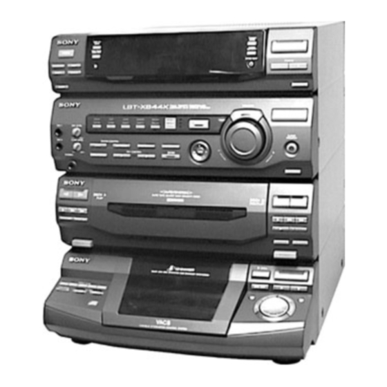
Photo: HCD-XB44
Model Name Using Similar Mechanism
CD
CD Mechanism Type
Section
Base Unit Name
Optical Pick-up Name
Model Name Using Similar Mechanism
Tape Deck
Section
Tape Transport Mechanism Type
SPECIFICATIONS
(HCD-XB33)
The following measured at AC 120/240 V, 50 Hz
DIN power output (Rated):
Continuous RMS power output (Reference):
Peak music power potput (Reference):
(HCD-XB44)
The following measured at AC 120/240 V, 50 Hz
DIN power output (Rated):
Continuous RMS power output (Reference):
Peak music power output (Reference):
COMPACT DISC DECK RECEIVER
US Model
HCD-D390/D790/G5500
Canadian Model
HCD-390/D790
AEP Model
UK Model
HCD-XB50/XB60
E Model
Australian Model
HCD-XB33/XB44
HCD-D290/
G3300/XB3
CDM37L-5BD29AL
BU-5BD29AL
KSS-213D/Q-NP
HCD-D290/
G3300/XB3
TCM-220WR2
100 + 100 watts (6 ohms at 1 kHz, DIN)
120 + 120 watts
(6 ohms at 1 kHz, 10% THD)
1,500 watts
120 + 120 watts (6 ohms at 1 kHz, DIN)
140 + 140 watts
(6 ohms at 1 kHz, 10% THD)
2,000 watts
— Continued on next page —
Advertisement
Table of Contents

Related Manuals for Sony HCD-D390 - Compact Audio And Video System


Summary of Contents for Sony HCD-D390 - Compact Audio And Video System
-
Page 1: Service Manual
With 8 ohm loads, both channels driven, from 70-20,000 Hz; rated 100 120 + 120 watts watts per channel minimum RMS power, with no more than 0.9 % total (6 ohms at 1 kHz, 10% THD) harmonic distortion from 250 milliwatts to rated output. - Page 2 PHONO IN (phono jacks): Tuning range sensitivity 3 mV, impedance 47 kilohms (2 band model) MIX MIC (phone jack): sensitivity 1 mV, impedance 10 kilohms North American model: 530 – 1,710 KHz (with the tuning interval set (HCD-D390/D790/G5500) at 10 kHz) VIDEO (AUDIO) IN (phono jacks): 531 –...
- Page 3 Leakage current can be measured by any one of three methods. • Do not touch the soldering iron on the same conductor of the circuit board (within 3 times). A commercial leakage tester, such as the Simpson 229 or RCA •...
-
Page 4: Table Of Contents
NOTES ON LASER DIODE EMISSION CHECK DECK Section ································································· 18 Tuner Section ··································································· 21 The laser beam on this model is concentrated so as to be focused on CD Section ······································································· 23 the disc reflective surface by the objective lens in the optical pick- up block. -
Page 5: General
&º ^¶ ^¡ ^™ ^£ ^¢ ^• ^ª ^§ ^∞ @¢ DECK B P (pause) button $• DECK A p (stop) button POWER button @∞ DECK B r REC button $ª DECK A 0 (backward) button DISPLAY/DEMO button %º @§... -
Page 6: Back Panel
⁄‚‡ ⁄‚fl ⁄‚fi XB33/XB44/XB50/XB60 MODEL ⁄‚› ⁄‚¤ ⁄‚‹ ⁄‚⁄ ANTENNA terminal ⁄‚¤ VOLTAGE SELECTOR switch (E, AR model) ⁄‚‹ SPEAKER terminal ⁄‚› SURROUND SPEAKER terminal (D790/XB33/XB50/XB60 model) ⁄‚fi VIDEO/MD (AUDIO) jack ⁄‚fl PHONO jack ⁄‚‡ CD DIGITAL OUT connector (XB33/XB44/XB50/XB60 model) - Page 7 This section is extracted from instruction manual. — 7 —...
-
Page 8: Disassembly
SECTION 2 DISASSEMBLY This set can be disassembled in the order shown below. UPPER FRONT PANEL MAIN CD MECHANISM OPTICAL BASE UNIT BD BOARD PICK-UP CASE SECTION SECTION DECK SECTION (Page 13) (Page 14) (Page 9) (Page 14) (Page 10) - Page 9 2 Four screws (BVTP 3 x 8) 2-3. MAIN BOARD 6 Back panel 4 Twelve screws 5 Power cord (BVTP 3 Fan is for (XB44 only) 3 Connector (CN901) 0 MAIN board IC201 9 Connector (CN105) (XB44 only) 1 Two flat wires...
- Page 10 2-4. MAIN SECTION 1 Flat wire (CN202) 2 Connector (CN203) 4 Main section 3 Two screws (BVTP 3 3 Screw (BVTP 3 3 Two screws (BVTP 3 2-5. CD MECHANISM DECK SECTION 3 Five screws (BVTP 3 4 CD mechanism...
- Page 11 TAPE MECHANISM DECK SECTION 4 Three screws 4 Three screws (BVTP 2.6 (BVTP 2.6 5 Remove the tape mechanism deck section to direction of the arrow A . 3 Two flat wires 2 Open the (CN601, 1001) cassette lid. 1 Push the two buttons.
- Page 12 4 Connector (CN661) 2 Four screws (BVTP 2.6 3 CD-B1 SW board 1 Connector (CN642) 2-9. PANEL (A) / (B) SUB ASSY 1 Connector (CN612) 3 Two claws 2 Four screws (BVTP 2.6 4 Panel (A) sub assy 5 Two claws 6 Panel (B) sub assy —...
- Page 13 2 Boss 2-11. DISC TABLE Note: When the disc table is installed, adjust the positions of roller cam and mark z as shown in the figure, then set to the groove of disc table. 3 Step screw 1 Screw (BVTP 3...
- Page 14 (BVTP 2.6 4 Flat wire (CN101) 6 Removal the four solders. 7 BD board Limit switch 2-13. OPTICAL PICK-UP, SLED MOTOR 3 Optical pick-up 4 Two screws (P 2 2 Sled shaft 1 Claw 5 Sled motor — 14 —...
- Page 15 2-14. AUDIO BOARD 2 Two rivets 1 Connector (CN651) 4 Four screws (BTP 2.6 3 Break the soldering of two flexible flat cables. 5 Audio board 2-15. CAPSTAN MOTOR 2 Two screws (BTP 2.6 4 Removal the capstan motor to direction of the arrow.
-
Page 16: Test Mode
“V” Value increases like 1, 2, 3 ... if rotating VOLUME knob 1. Press POWER button to turn the set ON. in “+” direction, or it decreases like 0, 9, 8 ... if rotating in “–” 2. Press PLAY MODE button and POWER button simulta- direction. - Page 17 4. FF is executed up to the end of tape. 1. Set discs in DISC 1 and DISC 3 trays. 5. A tape is reversed, and the tape on REV side is played for 2. Select the function “CD”. one minute.
-
Page 18: Mechanical Adjustments
3. Do not use a magnetized screwdriver for the adjustments. supply voltage unless otherwise noted. 4. After the adjustments, apply suitable locking compound to the 5. The adjustments should be performed in the order given in this parts adjusted. service manual. (As a general rule, playback circuit adjustment 5. - Page 19 2. Turn the adjustment screw and check output peaks. If the peaks do not match for L-CH and R-CH, turn the adjustment screw so Notes: • Start the Tape Speed adjustment as below after setting to the test mode. that outputs match within 1dB of peak.
- Page 20 Confirm playback that the signal recorded in step 1 becomes adjustable limits as follows. If these levels are not adjustable limits, adjust the RV1501 (L-CH) and RV1551 (R-CH) on the main board to repeat steps 1 and 2. — 20 —...
-
Page 21: Tuner Section
\Modulation: 999 kHz (at 9 kHz step) 1,050 kHz (at 10 kHz step) Procedure: 1. Set the output of SSG so that the input level of the set becomes Adjustment Location: TCB board 55 dB. 2. Tune the set to 999 kHz or 1,050 kHz. - Page 22 FM Polar Adjustment (East European, CIS model only) Procedure: 1. Set the modulation of FM RF SSG to AUDIO 1 kHz, 10 kHz Connection 1: deviation according to “Connection 1”. 2. Tune the set to 69 MHz. 3. Adjust the RV1702 so that the reading of frequency counter FM RF SSG connected to TP1702 (VCO) becomes within 31.25 kHz 0.05...
-
Page 23: Cd Section
6. After check, remove the lead wire connected in step 2. • RF signal Notes: • Try to measure several times to make sure than the ratio of A : B or B : A is more than 10 : 7. - Page 24 2. Turned Power switch on. TP (FEO) 3. Put disc (YEDS-18) in to play the number five track. 4. Press the “P (Pause)” button. (Becomes the 1 track jump mode) (GND) 5. Check the level B of the oscilloscope's waveform and the A IC103 (DC voltage) of the center of the Traverse waveform.
-
Page 25: Diagrams
HCD-D390/D790/G5500/XB33/XB44/XB50/XB60 SECTION 6 DIAGRAMS 6-1. CIRCUIT BOARD LOCATION 6-2. BLOCK DIAGRAMS – CD SECTION – TRANS board OPTICAL PICK-UP BLOCK X101 TCB board 16.9344MHz IC101(1/2) PANEL board FOCUS/TRACKING DETECTOR /SLED/SERVO RF AMP MAIN C,OUT CNIN LOUT1 MAIN board SECTION (page 31) -
Page 26: Tuner Section - (Aep, Uk Model)
HCD-D390/D790/G5500/XB33/XB44/XB50/XB60 – TUNER SECTION – (AEP, UK model) ST +10V FM FRONT END ANTENNA 10.7MHz 10.7MHz 10.7MHz IF AMP IF AMP FM 75 OUT L 19 AMP IN L ANT IN IF OUT 1 FM IN MPX IN FM DET OUT... -
Page 27: Tuner Section - (East European, Cis Model)
HCD-D390/D790/G5500/XB33/XB44/XB50/XB60 – TUNER SECTION – (East European, CIS model) ST +10V FM FRONT END ANTENNA 10.7MHz IF AMP 10.7MHz FM 75 OUT R ANT IN 1 FM IN 22 MPX IN IF OUT FM DET OUT Q1-4 COAXIAL OUT L... -
Page 28: Main Section
BIAS OSC T621 NORM BIAS Q623 SWITCH CROM X301 X302 Q301 5MHz 32.768KHz SECTION SWITCH 12 13 14 15 16 17 18 19 20 Q1001 Q1002 Q901 Q901 S1005 REEL REEL Q902 Q902 A CrO2 (page 26) SWITCH SWITCH IC302... - Page 29 4.8Vp-p 5.7Vp-p 5MHz under no-signal (detuned) conditions. 135.5 sec • Voltages are taken with a VOM (Input impedance 10 M ). Voltage variations may be noted due to normal produc- !¡ IC103 @¶ (MDP) IC103 *ª (XTAI) IC301 !¢ (XT1) tion tolerances.
-
Page 30: Printed Wiring Board - Bd Section
HCD-D390/D790/G5500/XB33/XB44/XB50/XB60 6-3. PRINTED WIRING BOARD – BD SECTION – • See page 25 for Circuit Boards Location. • Semiconductor (Component Side) (Conductor Side) Location Ref. No. Location IC101 IC102 IC103 Q101 MAIN BOARD CN202 (Page 67) • Indication of transistor These are omitted —... -
Page 31: Schematic Diagram - Bd Section
HCD-D390/D790/G5500/XB33/XB44/XB50/XB60 6-4. SCHEMATIC DIAGRAM – BD SECTION – • See page 34 for Waveforms. • See page 79 for IC Block Diagrams. — 37 — — 38 —... -
Page 32: Printed Wiring Board - Cd Motor Section
HCD-D390/D790/G5500/XB33/XB44/XB50/XB60 6-5. PRINTED WIRING BOARD – CD MOTOR SECTION – • See page 25 for Circuit Boards Location. PANEL BOARD CN203 (Page 67) — 39 — — 40 —... -
Page 33: Schematic Diagram - Cd Motor Section
HCD-D390/D790/G5500/XB33/XB44/XB50/XB60 6-6. SCHEMATIC DIAGRAM – CD MOTOR SECTION – — 41 — — 42 —... - Page 34 HCD-D390/D790/G5500/XB33/XB44/XB50/XB60 6-7. SCHEMATIC DIAGRAM – TUNER SECTION – (AEP, UK model) • See page 34 for Waveforms. • See page 83 for IC Block Diagrams. !£ !™ MAIN BOARD CN201 (Page 73) — 43 — — 44 —...
- Page 35 HCD-D390/D790/G5500/XB33/XB44/XB50/XB60 6-8. PRINTED WIRING BOARD – TUNER SECTION (AEP, UK Model) – • See page 25 for Circuit Boards Location. • Semiconductor Location Ref. No. Location D1751 IC21 IC41 IC1751 IC1752 MAIN BOARD CN201 (Page 68) • Indication of transistor These are omitted —...
- Page 36 HCD-D390/D790/G5500/XB33/XB44/XB50/XB60 6-9. PRINTED WIRING BOARD – TUNER SECTION (East European, CIS Model) – • See page 25 for Circuit Boards Location. • Semiconductor Location Ref. No. Location D1701 D1702 D1703 D1704 IC21 IC41 IC1701 IC1702 Q1701 Q1702 Q1703 MAIN BOARD...
- Page 37 HCD-D390/D790/G5500/XB33/XB44/XB50/XB60 6-10. SCHEMATIC DIAGRAM – TUNER SECTION – (East European, CIS model) • See page 34 for Waveforms. • See page 83 for IC Block Diagrams. !™ MAIN BOARD CN201 (Page 73) — 47 — — 48 —...
-
Page 38: Printed Wiring Board - Deck Section
HCD-D390/D790/G5500/XB33/XB44/XB50/XB60 6-11. PRINTED WIRING BOARD – DECK SECTION – • See page 25 for Circuit Boards Location. • Semiconductor Location Ref. No. Location IC601 IC602 IC611 H-11 Q621 Q622 Q623 Q651 F-10 Q1001 Q1002 MAIN BOARD CN206 (Page 67) MAIN BOARD... -
Page 39: Schematic Diagram - Deck Section
HCD-D390/D790/G5500/XB33/XB44/XB50/XB60 6-12. SCHEMATIC DIAGRAM – DECK SECTION – — 51 — — 52 —... -
Page 40: Schematic Diagram - Switch Section
HCD-D390/D790/G5500/XB33/XB44/XB50/XB60 6-13. SCHEMATIC DIAGRAM – SWITCH SECTION – — 53 — — 54 —... -
Page 41: Printed Wiring Board - Switch Section
HCD-D390/D790/G5500/XB33/XB44/XB50/XB60 6-14. PRINTED WIRING BOARD – SWITCH SECTION – • See page 25 for Circuit Boards Location. TC - A S W BO A RD T C-B SW BOA RD PANEL BOARD PANEL BOARD CN603 CN602 (Page 59) (Page 60) -
Page 42: Printed Wiring Board - Headphone-Mic Section
HCD-D390/D790/G5500/XB33/XB44/XB50/XB60 6-15. PRINTED WIRING BOARD – HEADPHONE-MIC SECTION – • See page 25 for Circuit Boards Location. • Semiconductor Location J760 J761 PHONES Ref. No. Location PANEL BOARD NO801 D671 (Page 60) D672 HEADP HONE-M IC B OARD D673 D674... -
Page 43: Schematic Diagram - Headphone-Mic Section
HCD-D390/D790/G5500/XB33/XB44/XB50/XB60 6-16. SCHEMATIC DIAGRAM – HEADPHONE-MIC SECTION – — 57 — — 58 —... -
Page 44: Printed Wiring Board - Panel Section
HCD-D390/D790/G5500/XB33/XB44/XB50/XB60 6-17. PRINTED WIRING BOARD – PANEL SECTION – • See page 25 for Circuit Boards Location. (P a ge 67 ) NO801 ( Pag e 5 6) D790/XB44/XB60 ( Pag e 55 ) C D-B1 SW B OARD N O811... -
Page 45: Schematic Diagram - Panel Section
HCD-D390/D790/G5500/XB33/XB44/XB50/XB60 6-18. SCHEMATIC DIAGRAM – PANEL SECTION – • See page 34 for Waveforms. • See page 86 for IC Pin Functions. — 61 — — 62 —... -
Page 46: Printed Wiring Board - Power Section
HCD-D390/D790/G5500/XB33/XB44/XB50/XB60 6-19. PRINTED WIRING BOARD – POWER SECTION – • See page 25 for Circuit Boards Location. (Page 67) (Page 67) CNP901 C807 (Page 68) — 63 — — 64 —... -
Page 47: Schematic Diagram - Power Section
HCD-D390/D790/G5500/XB33/XB44/XB50/XB60 6-20. SCHEMATIC DIAGRAM – POWER SECTION – C903 (XB50, XB60) — 65 — — 66 —... -
Page 48: Printed Wiring Board - Main Section
HCD-D390/D790/G5500/XB33/XB44/XB50/XB60 6-21. PRINTED WIRING BOARD – MAIN SECTION – • See page 25 for Circuit Boards Location. TCB BOARD M A I N BO AR D (Page 45, 46) XB50/ XB60 CD MOTOR BD BOARD C156 C155 R 158 XB33/ XB34/... -
Page 49: Schematic Diagram - Main Section (1/5)
HCD-D390/D790/G5500/XB33/XB44/XB50/XB60 6-22. SCHEMATIC DIAGRAM – MAIN SECTION (1/5) – • See page 82 for IC Block Diagrams. — 69 — — 70 —... -
Page 50: Schematic Diagram – Main Section (2/5)
HCD-D390/D790/G5500/XB33/XB44/XB50/XB60 6-23. SCHEMATIC DIAGRAM – MAIN SECTION (2/5) – • See page 81 for IC Block Diagrams. — 71 — — 72 —... -
Page 51: Schematic Diagram - Main Section (2/5)
HCD-D390/D790/G5500/XB33/XB44/XB50/XB60 6-24. SCHEMATIC DIAGRAM – MAIN SECTION (3/5) – • See page 34 for Waveforms. • See page 84 for IC Pin Functions. —73 — — 74 —... -
Page 52: Schematic Diagram – Main Section (4/5)
HCD-D390/D790/G5500/XB33/XB44/XB50/XB60 6-25. SCHEMATIC DIAGRAM – MAIN SECTION (4/5) – • See page 34 for Waveforms. • See page 82 for IC Block Diagrams. —75 — — 76 —... -
Page 53: Schematic Diagram - Main Section (3/5)
HCD-D390/D790/G5500/XB33/XB44/XB50/XB60 6-26. SCHEMATIC DIAGRAM – MAIN SECTION (5/5) – • See page 82 for IC Block Diagrams. — 77 — — 78 —... - Page 54 BAL1-4 TOG1-4 DFCT TZC COMP. 80 79 78 77 76 75 74 73 72 71 70 69 68 67 66 65 64 63 62 61 60 59 58 57 56 55 54 53 52 51 TDFCT SL_O TRACKING PHASE COMPENSATION...
-
Page 55: Main Section
– MAIN SECTION – IC102 MC14052BCP SELECT A INH 7 SELECT B IC201 M62427FP KEY IN2 BB22 SBAND GRAPHIC EQUALIZER – BPF OUT BUF IN1 – BPF IN BUF OUT1 IN 2B AVDD – – – DGND IN 2A LATCH –... - Page 56 IC281 UPC1237HA OVER LOAD DET MUTE OFFSET DET LATCH/ AUTORESET AC OFF IC901 LA5617 CURRENT CURRENT START ON/OFF ON/OFF LIMITER LIMITER CIRCUIT VREF VMUTE OVER HEAT PROTECT VREF ERROR VREF ~ _ 1.8V ERROR IIC1502 LB1641 T.S.D O.C.P MOTOR MOTOR...
-
Page 57: Tuner Section
– TUNER SECTION – IC21 LC72130 IC1701 IR3R42 19 18 14 13 PHASE COMPARATOR PHASE SWALLOW COUNTER PHASE COMPARATOR 2 1/16.1/17 4bits POWER TRIGGER REFERENCE RESET DIVIDER WAVEFORM SEP. SWALLOW COUNTER 1/16.1/17 4bits REGULATOR SAMPLE REFERENCE MUTE GATE & HOLD... -
Page 58: Ic Pin Function Description
6-28. IC PIN FUNCTION DESCRIPTION MAIN BOARD IC301 µPD780018Y (MAIN CONTROL) Pin No. Pin Name Function TA-MUTE Line mute signal output DBFB-H/L DBFB H/L select signal output 427-LT Latch signal output for IC201 (62427) KCON-LT Not used KCON-ON/OFF F-RELAY Front speaker relay control output... - Page 59 Up SW (S201) signal input ENC 3 ENC 2 Not used ENC 1 OUT-OPEN Not used CAP-M-H/N Capstan motor H/N speed select signal output B-TRG Trigger motor control output A-TRG Trigger motor control output TRG-LOW Trigger motor control output CAP-M-ON/OFF...
- Page 60 PANEL BOARD IC601 TMP87CH74 (DISPLAY CONTROL) Pin No. Pin Name Function 1–6 LED3-LED8 LED driver output – Ground X-OUT X’tal (8MHz) X-IN RESET Reset signal input from main controller LED 9 LED10 Connected ground TEST 14–19 LED11-LED19 LED driver output...
-
Page 61: Exploded Views
The components identified by mark ! or have some differences from the original one. in the exploded views are not supplied. dotted line with mark ! are critical for safety. • Items marked “*” are not stocked since they • Hardware (# mark) list and accessories and Replace only with part number specified. -
Page 62: Front Panel Section
1-669-631-11 CD-B1 SW BOARD X-4949-273-1 PANEL (A) SUB ASSY (D390/D790) X-4947-969-1 BUTTON (CD STOP) ASSY (G5500) X-4949-282-1 PANEL(A) SUB ASSY (XB33/XB44/XB50/XB60) X-4949-279-1 BUTTON (CD STOP) ASSY (EXCEPT G5500) * 55 1-664-012-11 TC-A SW BOARD 4-987-037-01 KNOB (JOG) (G5500) 4-986-999-01 BUTTON (EJECT A) (G5500) - Page 63 A-4403-872-A PANEL BOARD, COMPLETE 4-987-032-01 DISPLAY (TA) (D390/G5500/XB33/XB50: EE, CIS) 4-987-028-01 DISPLAY (ST)(G5500) * 119 A-4403-885-A PANEL BOARD, COMPLETE (XB60: AEP, UK) * 119 A-4403-892-A PANEL BOARD, COMPLETE (XB50: AEP, UK) 4-987-028-11 DISPLAY (ST) (EXCEPT G5500) 4-987-021-01 INDICATOR (TC A)
-
Page 64: Chassis Section
! CNP901 1-575-042-21 CORD, POWER (US, CND) * 154 A-4403-868-A POWER AMP BOARD, COMPLETE (XB60) ! CNP901 1-575-651-21 CORD, POWER (AEP, EE, AR, CIS, SAF, UK) * 154 A-4403-888-A POWER AMP BOARD, COMPLETE (XB44) ! CNP901 1-696-845-11 CORD, POWER (AUS) - Page 65 7-5. TAPE MECHANISM DECK SECTION-1 (TCM-220WR2) not supplied Ref. No. Part No. Description Remarks Ref. No. Part No. Description Remarks X-4947-943-1 HOLDER (L) ASSY, CASSETTE * 206 4-980-439-01 FULCRUM, HOLDER X-4947-944-1 HOLDER (R) ASSY, CASSETTE 3-354-957-01 JOINT (LOCK LEVER) 4-959-231-11 SPRING (L), TORSION...
- Page 66 3-917-142-01 SPRING, COMPRESSION 3-388-848-01 SCREW (P2X6) (B TIGHT) 3-911-116-11 RIVET, PUSH 3-939-371-01 SPRING (1), TENSION HP101 1-500-093-11 HEAD, MAGNETIC (PLAYBACK) (DECK A) X-3369-909-1 PINCH LEVER (REV) ASSY HRPE101 1-500-094-11 HEAD, MAGNETIC (REC/PB/ERASE) (DECK B) X-3369-908-1 PINCH LEVER (FWD) ASSY — 92 —...
- Page 67 7-7. TAPE MECHANISM DECK SECTION-3 (TCM-220WR2) r C : MOTOR board (supplied with AUDIO board) not supplied Ref. No. Part No. Description Remarks Ref. No. Part No. Description Remarks 3-908-597-01 CAM (A) X-3370-171-1 FLYWHEEL (BR) ASSY 3-908-608-11 SCREW, STEP 3-908-600-01 LEVER (REV-B)
- Page 68 7-8. CD MECHANISM DECK SECTION (CDM37L-5BD29AL) M201 BU-5BD29AL supplied Ref. No. Part No. Description Remarks Ref. No. Part No. Description Remarks 4-987-976-01 SCREW, STEP * 364 A-4673-765-A CD MOTOR BOARD, COMPLETE 4-944-490-01 BELT (TIMING) 4-978-426-01 INDICATOR (NO.) A-4660-978-A GEAR (PULLEY) ASSY...
- Page 69 Ref. No. Part No. Description Remarks ! 401 8-820-020-01 OPTICAL PICK-UP KSS-213D/Q-NP 4-917-564-01 GEAR (P), FLATNESS 1-769-069-11 WIRE (FLAT TYPE) (16 CORE) * 407 A-4699-522-A BD BOARD, COMPLETE 4-917-567-21 GEAR (M) 4-951-620-01 SCREW (2.6 8), +BVTP 4-951-940-01 INSULATOR (BU) M101...
-
Page 70: Electrical Parts List
METAL: metal-film resistor The components identified by mark ! or used on the set. METAL OXIDE: Metal Oxide-film resistor dotted line with mark ! are critical for safety. • -XX, -X mean standardized parts, so they may F: nonflammable Replace only with part number specified. - Page 71 1-126-607-11 ELECT CHIP 47uF C102 1-163-141-00 CERAMIC CHIP 0.001uF CNU101 1-770-014-11 CONNECTOR, FFC/FPC 16P C103 1-164-346-11 CERAMIC CHIP CNU102 1-778-874-11 CONNECTOR, FFC (LIF (NON-ZIF)) 19P C105 1-163-038-91 CERAMIC CHIP 0.1uF C106 1-164-161-11 CERAMIC CHIP 0.0022uF 10% 100V < FERRITE BEAD >...
- Page 72 1-216-061-00 METAL CHIP 3.3K 1/10W ************************************************************ R134 1-216-065-91 METAL CHIP 4.7K 1/10W R135 1-216-065-91 METAL CHIP 4.7K 1/10W A-4673-765-A CD MOTOR BOARD, COMPLETE R136 1-216-073-00 METAL CHIP 1/10W ************************** R137 1-216-065-91 METAL CHIP 4.7K 1/10W 4-980-385-01 HOLDER (SW) R138 1-216-025-91 METAL GLAZE...
- Page 73 CN661 1-506-481-11 PIN, CONNECTOR 2P 1-669-631-11 CD-B1 SW BOARD < SWITCH > *************** < CONNECTOR > S691 1-771-057-11 SWITCH, PUSH (1 KEY) (6 OPEN) * CN642 1-568-943-11 PIN, CONNECTOR 5P ************************************************************ < DIODE > A-4392-452-A HEADPHONE-MIC BOARD, COMPLETE ******************************* D645 8-719-057-10 DIODE LNJ301MPUJAB (·...
- Page 74 1-247-807-31 CARBON 1/4W A-4403-870-A MAIN BOARD, COMPLETE (XB60: AEP, UK) ********************* < VARIABLE RESISTOR > A-4403-890-A MAIN BOARD, COMPLETE (XB44: E, AR, MX) ********************* RV760 1-225-366-11 RES, VAR, CARBON 50K (MIC LEVEL) A-4403-894-A MAIN BOARD, COMPLETE (XB50: AEP, UK) ************************************************************...
- Page 75 C953 1-136-165-00 FILM 0.1uF (D790/XB44/XB60) C954 1-126-768-11 ELECT 2200uF C251 1-136-169-00 FILM 0.22uF C956 1-126-933-11 ELECT 100uF (D390/G5500/XB33/XB50) C1501 1-130-479-00 MYLAR 0.0047uF 5% C252 1-136-167-00 FILM 0.15uF C1502 1-162-290-31 CERAMIC 470PF (D790/XB44/XB60) C252 1-136-169-00 FILM 0.22uF (D390/G5500/XB33/XB50) — 101 —...
- Page 76 1-568-449-11 HOUSING, CONNECTOR (PC BOARD) 3P J101 1-695-188-31 JACK, PIN 4P (PHONO, VIDEO (AUDIO)) (D390/D790/G5500) < DIODE > J101 1-784-275-11 JACK, PIN 6P (PHONO, VIDEO (AUDIO)IN, OUT) (XB33/XB44/XB50/XB60) D141 8-719-991-33 DIODE 1SS133T-77 D191 8-719-991-33 DIODE 1SS133T-77 (XB44) < COIL >...
- Page 77 1-249-417-11 CARBON 1/4W F Les composants identifiés par The components identi- (XB50/XB60) une marque ! sont critiques fied by mark ! or dotted R152 1-249-417-11 CARBON 1/4W F pour la sécurité. line with mark ! are criti- Ne les remplacer que par une cal for safety.
- Page 78 1-249-441-11 CARBON 100K 1/4W R325 1-249-427-11 CARBON 6.8K 1/4W F R257 1-249-431-11 CARBON 1/4W (XB33: E, AR, MX/XB44: E, AR, MX/XB50: EE, CIS/XB60: EE, CIS) R325 1-249-431-11 CARBON 1/4W R259 1-249-441-11 CARBON 100K 1/4W (XB33: SAF, AUS/XB44: SAF, AUS) R260...
- Page 79 4.7K 1/4W F ********************** R1501 1-249-435-11 CARBON 1/4W (D390/G5500/XB33/XB50: EE, CIS) R1502 1-249-417-11 CARBON 1/4W F A-4403-885-A PANEL BOARD, COMPLETE (XB60: AEP, UK) R1503 1-249-426-11 CARBON 5.6K 1/4W ********************** A-4403-892-A PANEL BOARD, COMPLETE (XB50: AEP, UK) R1504 1-247-840-00 CARBON 2.4K...
- Page 80 D613 8-719-058-04 DIODE SEL5223S-TP15 (ENTER/NEXT) R613 1-249-401-11 CARBON 1/4W F D614 8-719-058-04 DIODE SEL5223S-TP15 (GROOVE) R614 1-249-429-11 CARBON 1/4W D615 8-719-058-04 DIODE SEL5223S-TP15 (SUPER WOOFER) (D790/XB44/XB60) R615 1-249-429-11 CARBON 1/4W R616 1-249-429-11 CARBON 1/4W D616 8-719-058-04 DIODE SEL5223S-TP15 (EFFECT) R617...
- Page 81 1-554-303-21 SWITCH, TACTILE (KARAOKE PON/MPX) R676 1-249-432-11 CARBON 1/4W S630 1-554-303-21 SWITCH, TACTILE (SURROUND) R677 1-249-436-11 CARBON 1/4W S631 1-554-303-21 SWITCH, TACTILE (P FILE MEMORY) R678 1-249-413-11 CARBON 1/4W F S634 1-554-303-21 SWITCH, TACTILE (PTY) R681 1-249-429-11 CARBON 1/4W (XB50: AEP, UK/XB60: AEP, UK)
- Page 82 1/4W F < CONNECTOR > R862 1-249-431-11 CARBON 1/4W R863 1-249-441-11 CARBON 100K 1/4W CN801 1-778-981-11 CONNECTOR, BOARD TO BOARD 13P ************************************************************ < DIODE > 1-659-058-13 TABLE SENSOR BOARD ******************* D801 8-719-991-33 DIODE 1SS133T-77 D841 8-719-991-33 DIODE 1SS133T-77 < IC >...
- Page 83 1-163-031-11 CERAMIC CHIP 0.01uF S656 1-554-303-21 SWITCH, TACTILE (P) S657 1-554-303-21 SWITCH, TACTILE (r REC) 1-163-139-00 CERAMIC CHIP 820PF S658 1-554-303-21 SWITCH, TACTILE (H SPEED DUB) 1-126-967-11 ELECT 47uF S659 1-554-303-21 SWITCH, TACTILE (CD SYNC) 1-163-031-11 CERAMIC CHIP 0.01uF 1-126-162-11 ELECT 3.3uF...
- Page 84 1-239-845-11 FILTER, LOW PASS * CN1 1-568-834-11 SOCKET, CONNECTOR 15P < TRANSISTOR > < TRIMMER > 8-729-201-27 TRANSISTOR 2SC2715Y CT1701 1-141-444-11 CAP, CERAMIC TRIMMER 50PF 8-729-201-27 TRANSISTOR 2SC2715Y CT1701 1-141-569-11 CAP, ADJ 50PF 8-729-201-27 TRANSISTOR 2SC2715Y 8-729-201-27 TRANSISTOR 2SC2715Y < DIODE >...
- Page 85 1-527-981-00 FILTER, CERAMIC (450kHz) 1-216-065-00 METAL CHIP 4.7K 1/10W ************************************************************ 1-216-037-00 METAL CHIP 1/10W 1-216-001-00 METAL CHIP 1/10W A-4303-590-A TCB BOARD, COMPLETE (AEP, UK) 1-247-843-11 CARBON 3.3K 1/4W F ******************** 1-216-065-00 METAL CHIP 4.7K 1/10W < CAPACITOR > 1-216-097-91 METAL CHIP...
- Page 86 8-719-016-74 DIODE 1SS352-TPH3 1-216-037-00 METAL CHIP 1/10W 1-216-037-00 METAL CHIP 1/10W < FRONT-END > 1-216-081-00 METAL CHIP 1/10W 1-693-357-11 FRONT END (4 GANG) 1-216-037-00 METAL CHIP 1/10W 1-233-514-11 ENCAPSULATED COMPONENT 1-216-037-00 METAL CHIP 1/10W 1-216-081-00 METAL CHIP 1/10W < IC >...
- Page 87 3.3K 1/10W ! CNP901 1-575-042-21 CORD, POWER (US, CND) 1-216-061-00 METAL CHIP 3.3K 1/10W ! CNP901 1-575-651-21 CORD, POWER (AEP, EE, AR, CIS, SAF, UK) 1-216-073-00 METAL CHIP 1/10W ! CNP901 1-696-845-11 CORD, POWER (AUS) 1-216-061-00 METAL CHIP 3.3K 1/10W...
- Page 88 ! CNP901 1-558-943-51 CORD, POWER (E, MX) (FRENCE, SPANISH, PORTUGUESE) ! CNP901 1-575-042-21 CORD, POWER (US, CND) 3-862-180-81 MANUAL, INSTRUCTION (EE, CIS) ! CNP901 1-575-651-21 CORD, POWER (AEP, EE, AR, CIS, SAF, UK) (RUSSIAN, POLISH) 3-862-181-11 MANUAL, INSTRUCTION ! CNP901 1-696-845-11 CORD, POWER (AUS)
Need help?
Do you have a question about the HCD-D390 - Compact Audio And Video System and is the answer not in the manual?
Questions and answers