Table of Contents
Advertisement
Quick Links
Preliminary Datasheet
This document provides an overview of e2v's VITA 57 FMC Quad 8-bit ADC Demo Kit.
Main Features
•
Sampling of analog signals using EV8AQ160 Quad 8-bit ADC
•
4 analog inputs with different configurations
Differential driver (2 types of amplifier provided)
o
Balun RF transformer.
o
Direct input.
o
•
Clock Input:
External clock
o
or/ programmable clock generated by a PLL (2.4G to 2.7 Gsps)
o
•
Interfacing ADC Digital outputs with an external acquisition system either with
A logic analyzer
o
An FPGA development board using the VITA57 FMC standard
o
http://www.vita.com/fmc.html
•
100% compatible with XILINX VIRTEX 6 evaluation kit ML605
http://www.xilinx.com/products/devkits/EK-V6-ML605-G.htm
o
•
FFT computation (PC software provided)
•
Flexible and easy to operate via USB2 control (PC software provided without any license)
•
Programming of ADC settings
•
Programming of ADC environment
•
Monitoring of ADC currents and junction temperature
•
Universal 12V power Adapter
Operating conditions
Temperature range: 10° C < Tamb < 40° C
Operating with a Microsoft Windows PC environment (Windows 2000, Windows XP, Windows
Vista) via USB interface.
BDC- 1-Sep-10
VITA 57 FMC Quad 8-bit ADC Demo Kit
EV8AQ160TPY-DK
EV8AQ160
e2v semiconductors SAS 2010
1
Advertisement
Table of Contents

Subscribe to Our Youtube Channel
Related Manuals for e2v EV8AQ160

Summary of Contents for e2v EV8AQ160
-
Page 1: Preliminary Datasheet
EV8AQ160TPY-DK EV8AQ160 VITA 57 FMC Quad 8-bit ADC Demo Kit Preliminary Datasheet This document provides an overview of e2v’s VITA 57 FMC Quad 8-bit ADC Demo Kit. Main Features • Sampling of analog signals using EV8AQ160 Quad 8-bit ADC •... -
Page 2: General Overview
Since this Development Kit is intended to be used on an industrial workbench and modified by the user to build his prototypes, NO WARRANTY OF ANY KIND can apply. NO LIABILITY will be accepted by e2v, whatsoever may arise as a result of the use of these boards. BDC- 1-Sep-10... -
Page 3: Quad 8-Bit Adc
Figure 1. EV8AQ160 Quad 8-bit ADC Block diagram The EV8AQ160 Quad ADC is built with four 8-bit ADC cores which can be used either independently (four-channel mode) or group by two cores (two-channel mode with the ADCs interleaved two by two) or one-channel mode where all four ADCs are all interleaved. -
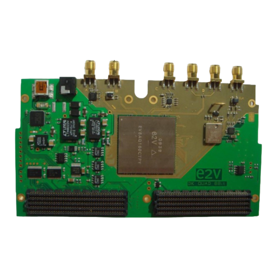
Page 4: Demo Kit
VITA57 interface FPGA 12V supply adapter (VIRTEX 6) The complete system is built with the e2v demo kit and an FPGA development kit. e2v Demo kit contains the following items : • Quad 8-bit Demo kit with EV8AQ160CTPY • Cables & Power Supply Universal 12V power Adapter &... - Page 5 A USB driver on the ADC Demo kit allows for transmission of the data to the computer that performs the display and processing of ADC output data (FFT). Software and Graphical User Interface are provided with the Demo Kit. The provided software operates using Labview RunTime (no license required). BDC- 1-Sep-10 e2v semiconductors SAS 2010...
-
Page 6: Quick Start
Check if the Xilinx FPGA evaluation board ML605 is properly configured with correct software. • Check Demo Kit BDC QUAD 8bit is properly plugged into FPGA connector. • Check if USB connector is properly plugged. BDC- 1-Sep-10 e2v semiconductors SAS 2010... -
Page 7: Measurement
Warning: FFT with no windowing with no coherent signal: you could have this kind of signal Warning: if the Fin frequency have value exact like 250 MHz the FTT result is wrong it is why it is recommend doing measurements with shift of 2MHz like 252 MHz. BDC- 1-Sep-10 e2v semiconductors SAS 2010... - Page 8 With channel A and channel C (with amplificatory) it is needed to add RF attenuator on SMA connecter to have optimum performance. • • Check the temperature of QUAD ADC < 105° C and heatsink is properly connected BDC- 1-Sep-10 e2v semiconductors SAS 2010...
-
Page 9: External Equipment
For optimum performance this generator must have a low phase noise Please see example of signal generator • Cables & Power Supply (provided by e2v) Universal 12V power Adapter & Cables USB Cables to communicate with a PC (control of ADC settings and settings for data acquisition) •... -
Page 10: Main Functions
Single to Differential Amplifier from Analog Devices (C channel: ADA4939-1) • Direct input via SMA connector (D channel) (free for customer use) Figure 5. Analog input SMA configuration D channel A channel C channel B channel Ext Clock BDC- 1-Sep-10 e2v semiconductors SAS 2010... -
Page 11: Analog Input Channel A
This LMH6555 could be used in AC configuration Please see chap 6.1 Channel A 3.1.2. Analog input Channel B The Analog input channel A uses an RF Transformer from Coilcraft ref: WBC4_1WLB http://www.coilcraft.com/pn/WBC4-1WLB.htm Figure 7. Channel B : schematic BDC- 1-Sep-10 e2v semiconductors SAS 2010... -
Page 12: Analog Input Channel C
Analog input Channel D This channel is free for customer use in differential and AC coupling configuration. Figure 9. Channel D : schematic This Channel D could be used in DC configuration Please see chap 6.3 Channel BDC- 1-Sep-10 e2v semiconductors SAS 2010... -
Page 13: Adc Clock Input Signal
3.3. Control of ADC settings The Graphical User Interface allows for complete monitoring and control of all the settings of EV8AQ160 Quad 8-bit ADC such as channel selection, Gain, Offset, Phase, test mode (with SPI signal). Please see chap 4.5 Operating Modes. -
Page 14: Adc Junction Temperature Monitoring
The Demo kit provides an external heat sink to stabilize the junction temperature in under 110° C. Heat sink from AAVID THERMALLOY ref: 374724B00032G 35 x 35 x 18 http://www.aavidthermalloy.com/cgi-bin/ bga_disp.pl?partnum=043184&size=35&height=18&pkg=Metal&length=35&nc=15.3&fc=5.15 This heat sink should be fixed to the ADC QUAD 8bit with a thermal conductive foil both side adhesive. BDC- 1-Sep-10 e2v semiconductors SAS 2010... -
Page 15: Adc Current Consumption Monitoring
FX2 and the D950LV0011 devices transform the single ended signal into an LVDS signal. Figure 13. ADC SYNC signal Note: By default, the SYNC signal via FX2 is selected but SYNC signal via the FPGA is allowed. Please see chap 6.6 SYNC signal. BDC- 1-Sep-10 e2v semiconductors SAS 2010... -
Page 16: Dc/Dc Converter
The power supply for the QUAD 8bit is provided by DC/DC block from Linear Technologies. • Vcc (3V3) power supply with micro module LTM8023 http://www.linear.com/pc/productDetail.jsp?navId=H0,C1,C1003,C1424,P39569 • Vcco and Vccd (1.8V) power supply with micro module LTM8021 http://www.linear.com/pc/productDetail.jsp?navId=H0,C1,C1003,C1042,C1424,P81177 Figure 14. Power supplies 3V3A Figure 15. Power supplies 1.8V BDC- 1-Sep-10 e2v semiconductors SAS 2010... -
Page 17: Software Tools
FPGA software The Demo Kit board can be plugged with XILINX VIRTEX 6 evaluation board EK-V6-ML605-G http://www.xilinx.com/products/devkits/EK-V6-ML605-G.htm e2v provides FPGA program to be used with QUAD 8bit Demo-Kit. • User interface software The user interface software is a Visual C++ compiled graphical interface that does not require a licence to run on a Windows NT and Windows 2000/98/XP PC. -
Page 18: User Interface Installation
EV8AQ160-DK 4.3. User Interface installation 1. Install the Demo kit EV8AQ160 application on your computer by launching the SetupEvalkitQuadAdc8Bits.exe installer (please refer to the latest version available). The screen shown in Figure 5 is displayed: Figure 16. demo kit QUAD 8bit application “Setup wizard” window 2. - Page 19 EV8AQ160TPY-DK 3. Select Components (Start Menu Folder) Figure 18. demo kit QUAD 8bit application “Start Menu Folder” 4. Select Components (Additional Tasks) Figure 19. demo kit QUAD 8bit application “Additional Tasks” BDC- 1-Sep-10 e2v semiconductors SAS 2010...
- Page 20 Now a new process of installation started Processing&Display for installing Labview RunTime (no license required. Please follow instruction. Warning: don’t press finish button on “Completing Setup wizard” window. The screen shown in Figure 21 is displayed: BDC- 1-Sep-10 e2v semiconductors SAS 2010...
- Page 21 EV8AQ160TPY-DK 6 Select Components Processing&Display (installation Wizard) Figure 21. demo kit QUAD 8bit Processing&Display “installation Wizard” 7 Select Components Processing&Display (Destination Folder) Figure 22. demo kit QUAD 8bit Processing&Display “Destination Folder” BDC- 1-Sep-10 e2v semiconductors SAS 2010...
- Page 22 The installation of the software is now completed but you need to launch the Processing&Display software. This installation launch automatically. 9 Select Components Processing&Display (Completing Setup wizard” window) Figure 24. demo kit QUAD 8bit Processing&Display “Completing Setup wizard” window” BDC- 1-Sep-10 e2v semiconductors SAS 2010...
- Page 23 QUAD 8bit application “Completing Setup wizard” window” Note README message. Please follow instruction before using Demo kit QUAD 8bit application. Figure 26. README message Please see chap 4.5.11. Regional and Language Options. BDC- 1-Sep-10 e2v semiconductors SAS 2010...
-
Page 24: Usb Driver Installation
The window shown in Figure 27 will be displayed. Figure 27. Install driver software Please choose: Locate and install driver software (recommended) Figure 28. Allow Windows to search driver Please choose: Yes, always search online (recommended) BDC- 1-Sep-10 e2v semiconductors SAS 2010... - Page 25 EV8AQ160TPY-DK Figure 29. Browse the driver software Please choose: Browse my computer for driver software (advanced) Figure 30. Choose the folder Select C:\Program Files\E2V\EvalkitQuadAdc8Bits BDC- 1-Sep-10 e2v semiconductors SAS 2010...
- Page 26 EV8AQ160-DK Figure 31. Warning: installation Please choose: Install the driver software anyway A Data transfer has been beginning please wait Figure 32. END of new Driver installation The new driver has been installed BDC- 1-Sep-10 e2v semiconductors SAS 2010...
- Page 27 USB driver before used. After the installation, you can launch the interface with the following file: C:\Program Files\E2V\EvalkitQuadAdc8Bits\EvalkitQuadAdc8Bits.exe The window shown in Figure 15 will be displayed. Figure 33. User Interface Demo Kit BDC- 1-Sep-10 e2v semiconductors SAS 2010...
-
Page 28: Operating Modes
Clicking the “Cancel” button will restore last settings sent with “Apply” button. With Gain/Offset/Phase and INL windows always click on “Write” then “Send” buttons to validate any command. The Reset button allows re-configuring ADC to the Default Mode. BDC- 1-Sep-10 e2v semiconductors SAS 2010... - Page 29 This User interface could be reduced using “Hide Tab”, below. User Interface Demo Kit with Hide Tab configuration Figure 34. This User Interface Demo show the Chip ID of QUAD 8bit at the bottom right corner Figure 35. Chip ID of QUAD 8bit BDC- 1-Sep-10 e2v semiconductors SAS 2010...
-
Page 30: Setting
EV8AQ160-DK 4.5.1. Setting In this window, 5 functions are available: ADC mode: General Standby Synchronization Reset BDC- 1-Sep-10 e2v semiconductors SAS 2010... - Page 31 1 channel mode = the 4 ADCs are all interleaved, the sampling rate is Fclock x 2 (where Fclock is the external clock signal frequency), the analogue input can be applied to either A, B, C or D channel. BDC- 1-Sep-10 e2v semiconductors SAS 2010...
- Page 32 No standby = all channels are active (A: ON, B: ON, C: ON, D: ON); Partial standby = either A & B are in standby or C & D are in standby; Full standby = all 4 ADCs are in standby. BDC- 1-Sep-10 e2v semiconductors SAS 2010...
-
Page 33: Test
A flashing bit is generated with on bit at 1 within each ADC and output follow with ten bit at 0 ( 1 FF pattern every ten 00 patterns) FPGA Test (for testing communication between Demo kit and FPGA) : ramp test BDC- 1-Sep-10 e2v semiconductors SAS 2010... - Page 34 EV8AQ160-DK Gain / Offset / Phase In this window, you can adjust the gain, offset and phase of the channel selected via the “channel select” button on the top right of the user interface. BDC- 1-Sep-10 e2v semiconductors SAS 2010...
- Page 35 In the following example, you can see that the internal Gain register is set to 0.059 and that the user wants the phase to be set to -15. In the second picture, the WRITE and SEND buttons have been pushed and the internal register shows the new entered value for the phase BDC- 1-Sep-10 e2v semiconductors SAS 2010...
-
Page 36: Input Impedance
WRITE button to write these values to the internal registers (you can retrieve the initial value of the impedance by clicking on the CANCEL button). This function helps to re-adjust the input impedance in case of a slight mismatch due to temperature variations or process variations. BDC- 1-Sep-10 e2v semiconductors SAS 2010... -
Page 37: Inl
ON and READY (green LEDs); write the INL values in the Ext INL1 and Ext INL2 boxes; If you need to retrieve the old value of INL click CANCEL BDC- 1-Sep-10 e2v semiconductors SAS 2010... - Page 38 WRITE button to write these values to the internal registers; push the SEND button to perform the calibration; The calibration is successful if the Ext INL1 and INL1 boxes display the same values. BDC- 1-Sep-10 e2v semiconductors SAS 2010...
- Page 39 EV8AQ160TPY-DK INL Calibration procedure: Push “Load File” bottom in INL calibration Select file BDC- 1-Sep-10 e2v semiconductors SAS 2010...
- Page 40 The INL measurement must be done for each channel (at low analog input frequency). For each channel, you must create one file per ADC channel. File txt format with 256 INL code. Example ADC_QUAD_INL.txt BDC- 1-Sep-10 e2v semiconductors SAS 2010...
- Page 41 For this example select a channel (ex A). After load file, the software computes automatically the INL register. Note. Don’t forget to push write and send button. After Channel A repeat the same procedure for channel B, C and D. BDC- 1-Sep-10 e2v semiconductors SAS 2010...
-
Page 42: Clock
The capture of data QUAD 8bit at full speed must be done only in 1:2 Dmux mode. The capture of data QUAD 8bit at in 1:1 Dmux mode could be done with Fclock lower than 2GHz. BDC- 1-Sep-10 e2v semiconductors SAS 2010... - Page 43 • Normal mode 2.4GHz up to 2.7GHz • Divided par 2 mode 1.2 GHz up to 1.35 GHz Selection of PLL power When external clock has been chosen, the clock frequency must be specified. BDC- 1-Sep-10 e2v semiconductors SAS 2010...
-
Page 44: Power
EV8AQ160-DK 4.5.6. Power This sheet allows measurement of the QUAD 8bit power consumption and the internal temperature junction. BDC- 1-Sep-10 e2v semiconductors SAS 2010... - Page 45 EV8AQ160TPY-DK Power when DMUX by 2 is selected Power when DMUX by 1 is selected Power when standby full is selected BDC- 1-Sep-10 e2v semiconductors SAS 2010...
-
Page 46: Acquisition Control
EV8AQ160-DK 4.5.7. Acquisition control This sheet controls the acquisition modes of the QUAD 8bit BDC- 1-Sep-10 e2v semiconductors SAS 2010... - Page 47 FFT windows to perform a correct result. Peak width: When FFT windows is applied the Harmonic signal is composed of several points Default value: 11 You can save data in an excel file Select directory BDC- 1-Sep-10 e2v semiconductors SAS 2010...
-
Page 48: Acquisition
When you launch acquisition several window results appear CH_A => ADC channel A CH_B => ADC channel B CH_C => ADC channel C CH_D => ADC channel D Sample signal: example of signal in simultaneous channel BDC- 1-Sep-10 e2v semiconductors SAS 2010... - Page 49 EV8AQ160TPY-DK INL Curve: FFT spectrum BDC- 1-Sep-10 e2v semiconductors SAS 2010...
- Page 50 EV8AQ160-DK FFT parameters Plot selection: you can select one channel or several for easier reading BDC- 1-Sep-10 e2v semiconductors SAS 2010...
- Page 51 EV8AQ160TPY-DK Zoom selection: You can choose several kind of zoom Lock selection: Cursor selection: and move cursor on channel BDC- 1-Sep-10 e2v semiconductors SAS 2010...
- Page 52 − MaxRaie SFDR fondamenta − − BruitMoyen SINAD − − − SINAD ENOB SFSR dBFS − SFSR dBFS SFDR SFDR SFSR dBFS − − SINAD log( dBFS dBFS dBFS − SINAD ENOB dBFS dBFS BDC- 1-Sep-10 e2v semiconductors SAS 2010...
- Page 53 SFDR SFDR SFSR dBFS − − SINAD log( dBFS dBFS dBFS − SINAD dBFS ENOB dBFS The parameters with the _FS prefix correspond to the same parameter but in dBFS (from full scale). BDC- 1-Sep-10 e2v semiconductors SAS 2010...
-
Page 54: Demo Kit Configuration File
It is possible to save the context of the Demo Kit (saving of all settings and configuration). This context can be saved for later use, so that saved settings can be reloaded. File DK BDC QUAD8bit Conf.ctx Figure 36. example of context of the Demo Kit BDC- 1-Sep-10 e2v semiconductors SAS 2010... -
Page 55: Data Save File
Warning: before using you need to configure your PC. The decimal separator must be a dot “.” instead of comma “,” like in French. Use a control Regional Setting to check if decimal separator is configured with a dot “.”. BDC- 1-Sep-10 e2v semiconductors SAS 2010... -
Page 56: Regional And Language Options
EV8AQ160-DK 4.5.11. Regional and Language Options Use a control Regional Setting to check if decimal separator is configured with a dot “.”. Figure 38. Regional and Language Options Selection: Customize this format. BDC- 1-Sep-10 e2v semiconductors SAS 2010... - Page 57 EV8AQ160TPY-DK Figure 39. Customize regional Option Sheet Numbers The decimal separator must be configured with a dot “.” BDC- 1-Sep-10 e2v semiconductors SAS 2010...
-
Page 58: Fpga Code
The FPGA code has been designed to be used with ML605 Xilinx Virtex 6 evaluation board Warning Please configure your LM605 evaluation board with correct Switch configuration 5.1. Software configuration XILINX configuration: VIRTEX-6 FPGA ML605 Evaluation Kit Xilinx ISE Design Suite version 12 or upper with IMPACT software BDC- 1-Sep-10 e2v semiconductors SAS 2010... -
Page 59: Fpga Programming
Change the Configuration Mode Switch and System ACE Address Lunch the iMPACT of ISE suite and load the auto_project.ipf Target FPGA: Virtex6 BPI Flash: xcf128x [16] Load DK_QUAD_8.pif info XILINX Virtex 6 Load DK_QUAD_8.mcs info Flash BDC- 1-Sep-10 e2v semiconductors SAS 2010... -
Page 60: Vhdl Code
B [BL BH] SERDES FIFO C [CL CH] SERDES FIFO D [DL DH] FIFO SERDES Reg File VHDL simplify SERDES diagram for each ADC output bit I/O Buff DDR clock FIFO BUFR/4 I/O Buff Output Data BDC- 1-Sep-10 e2v semiconductors SAS 2010... -
Page 61: Demo Kit Hardware Configuration
For positive shift, a positive current would be injected into VIN+ R107 must be used. For negative shift, a negative current would be injected into VIN- R108 must be used. TOP VIEW BDC- 1-Sep-10 e2v semiconductors SAS 2010... -
Page 62: Channel C
The gain of differential ADC driver could be changed by altering the values of R40, R43, R44 and R45. TOP VIEW 6.3. Channel D The Chanel D could be used in DC configuration mode by replacing C126 and C127 by a 0Ω resistor. BDC- 1-Sep-10 e2v semiconductors SAS 2010... - Page 63 EV8AQ160TPY-DK BDC- 1-Sep-10 e2v semiconductors SAS 2010...
-
Page 64: Clock Selection
Remove R15 and R37 resistor and solder R36 and R50 with a 0Ω. Note: The code supplied permits operation at 2.5 GHz a re-compilation with different timing constraints will be required for other frequencies. TOP VIEW BDC- 1-Sep-10 e2v semiconductors SAS 2010... -
Page 65: Spi Signal
The selection between the two clocks is done manually with a resistor. Note: e2v doesn’t provide the SPI controller FPGA code. Remove R93, R95, R97, R99 and R101 resistor and solder R94, R96, R98, R100 and R102 with a 0Ω. -
Page 66: Sync Signal
The SYNC signal is control by FX2 microcontroller, but this signal could be controlled by the FPGA. The selection between the two clocks is done manually with a resistor. Note: e2v doesn’t provide the SYNC signal FPGA code. Remove R105 resistor and solder R106 with a 0Ω. -
Page 67: Electrical Schematic
EV8AQ160TPY-DK 7 Electrical schematic Figure 40. Power supplies management” BDC- 1-Sep-10 e2v semiconductors SAS 2010... - Page 68 EV8AQ160-DK Figure 41. Temperature sense and current measurement” BDC- 1-Sep-10 e2v semiconductors SAS 2010...
- Page 69 EV8AQ160TPY-DK Figure 42. FX2 microcontroller and ADC level shifting” BDC- 1-Sep-10 e2v semiconductors SAS 2010...
- Page 70 EV8AQ160-DK Figure 43. ADC QUAD 8bit signal configuration and decoupling capacitor ” BDC- 1-Sep-10 e2v semiconductors SAS 2010...
- Page 71 EV8AQ160TPY-DK Figure 44. Analog input configuration and SYNC signal ” BDC- 1-Sep-10 e2v semiconductors SAS 2010...
- Page 72 EV8AQ160-DK Figure 45. Output connector HPC port A and Port B BDC- 1-Sep-10 e2v semiconductors SAS 2010...
- Page 73 EV8AQ160TPY-DK Figure 46. Clock configuration and PLL BDC- 1-Sep-10 e2v semiconductors SAS 2010...
- Page 74 EV8AQ160-DK Figure 47. Output connector HPC port C and Port D BDC- 1-Sep-10 e2v semiconductors SAS 2010...
- Page 75 EV8AQ160TPY-DK Figure 48. Level shifting VITA EEPROM Power good generation BDC- 1-Sep-10 e2v semiconductors SAS 2010...
-
Page 76: Layout Information
EV8AQ160-DK 8 Layout information Figure 49. Top side Layer 1 Figure 50. internal Layer 2 BDC- 1-Sep-10 e2v semiconductors SAS 2010... - Page 77 EV8AQ160TPY-DK Figure 51. internal Layer 3 Figure 52. internal Layer 4 BDC- 1-Sep-10 e2v semiconductors SAS 2010...
- Page 78 EV8AQ160-DK Figure 53. internal Layer 5 Figure 54. internal Layer 6 BDC- 1-Sep-10 e2v semiconductors SAS 2010...
- Page 79 EV8AQ160TPY-DK Figure 55. internal Layer 7 Figure 56. internal Layer 8 BDC- 1-Sep-10 e2v semiconductors SAS 2010...
- Page 80 EV8AQ160-DK Figure 57. internal Layer 9 Figure 58. internal Layer 10 BDC- 1-Sep-10 e2v semiconductors SAS 2010...
- Page 81 EV8AQ160TPY-DK Figure 59. internal Layer 11 Figure 60. bottom side Layer 12 BDC- 1-Sep-10 e2v semiconductors SAS 2010...
-
Page 82: Mechanical Dimensions
EV8AQ160-DK 9 Mechanical dimensions The Demo Kit board with Quad 8-bit ADC dimension is 139mm x 76.5mm x 8mm. It is compatible with VITA57 FMC standard. Figure 61. Mechanical dimension Double Width BDC- 1-Sep-10 e2v semiconductors SAS 2010... -
Page 83: Ordering Information
EV8AQ160TPY-DK 10 Ordering Information Table 1. Ordering information Package Temperature Screening Comments Part Number Used with EV8AQ160TPY-DK EBGA380 Ambient Prototype XILINX VIRTEX 6 evaluation kit ML605 BDC- 1-Sep-10 e2v semiconductors SAS 2010... -
Page 84: Table Of Contents
Channel C............................... 62 6.3. Channel D............................... 62 6.4. Clock selection..............................64 6.5. SPI signal ............................... 65 6.6. SYNC signal ..............................66 7 Electrical schematic ......................67 8 Layout information ......................76 9 Mechanical dimensions ....................82 10 Ordering Information.....................83 BDC- 1-Sep-10 e2v semiconductors SAS 2010...
Need help?
Do you have a question about the EV8AQ160 and is the answer not in the manual?
Questions and answers