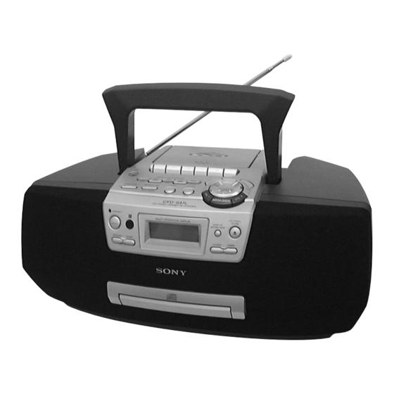
Sony CFD-S47 Service Manual
Cd radio cassette-corder
Hide thumbs
Also See for CFD-S47:
- Operating instructions manual (36 pages) ,
- Specifications (2 pages) ,
- Limited warranty (1 page)
Table of Contents
Advertisement
Quick Links
SERVICE MANUAL
Ver 1.0 1998. 12
AUDIO POWER SPECIFICATIONS (US Model)
POWER OUTPUT AND TOTAL
HARMONIC DISTORTION
With 6-ohm loads, both channels driven
from 100 - 10,000 Hz: rated 3.5 W per
channel-minimum RMS power, with no more
than 10% total harmonic distortion in AC
operation.
CD player section
System
Compact disc digital audio system
Laser diode properties
Material: GaAlAs
Wave length: 780 nm
Emission duration: Continuous
Laser output: Less than 44.6 µW
(This output is the value measured at a distance of
about 200 mm from the objective lens surface on
the optical pick-up block with 7 mm aperture.)
Spindle speed
200 r/min (rpm) to 500 r/min (rpm) (CLV)
Number of channels
2
Frequency response
20 - 20,000 Hz +1/–2 dB
Wow and flutter
Below measurable limit
MICROFILM
CFD-S47
Model Name Using Similar Mechanism NEW
CD Loading Mechanism Type
CD
Section CD Mechanism Type
Optical Pick-up Name
Model Name Using Similar Mechanism CFD-V10
TC
Section Tape Transport Mechanism Type
SPECIFICATIONS
Radio section
Frequency range
FM
US, E model
Singapore model
AM
US, E model
Singapore model
IF
FM: 10.7 MHz
AM: 450 kHz
Aerials
FM: Telescopic aerial
AM: Built-in ferrite bar aerial
Cassette-corder section
Recording system
4-track 2 channel stereo
Fast winding time
Approx. 150 sec. with Sony cassette C-60
Frequency response
TYPE I (normal): 80 - 10,000 Hz
CD RADIO CASSETTE-CORDER
– 1 –
US Model
E Model
FLM-S47-149
KSM-213CCP
KSS-213C
MF-V10-117
87.6 - 108 MHz
87.6 - 107 MHz
530 - 1,710 kHz
531 - 1,602 kHz
– Continued on next page –
Advertisement
Table of Contents

Related Manuals for Sony CFD-S47


Summary of Contents for Sony CFD-S47
- Page 1 Emission duration: Continuous Fast winding time Laser output: Less than 44.6 µW Approx. 150 sec. with Sony cassette C-60 (This output is the value measured at a distance of Frequency response about 200 mm from the objective lens surface on TYPE I (normal): 80 - 10,000 Hz the optical pick-up block with 7 mm aperture.)
- Page 2 COMPONENTS IDENTIFIED BY MARK ! OR DOTTED LINE WITH MARK ! ON THE SCHEMATIC DIAGRAMS AND IN THE PARTS LIST ARE CRITICAL TO SAFE OPERATION. REPLACE THESE COMPONENTS WITH SONY PARTS WHOSE PART NUMBERS APPEAR AS SHOWN IN THIS MANUAL OR IN SUPPLEMENTS PUBLISHED BY SONY.
-
Page 3: Table Of Contents
SAFETY CHECK-OUT TABLE OF CONTENTS 1. GENERAL After correcting the original service problem, perform the following safety check before releasing the set to the customer: Playing a CD ................4 Check the antenna terminals, metal trim, “metallized” knobs, screws, Listening to the radio ............... 4 and all other exposed metal parts for AC leakage. - Page 4 SECTION 1 GENERAL This section is extracted from instruction manual. – 4 –...
- Page 5 – 5 –...
-
Page 6: Disassembly
SECTION 2 DISASSEMBLY • The equipment can be removed using the following procedure. Cabinet (front) Cabinet (upper) CD mechanism SW (L) board, assy assy block SW (R) board Tuner board Plate assy, Tray Loading chuck board board mechanism Power board block Main SW (TOP) board,... -
Page 7: Cabinet (Upper) Assy
2-3. CABINET (UPPER) ASSY 6 cabinet (upper) assy 2 CNP307 4 BVTP 3x10 1 CNP1 5 CNP501 3 CNP702 2-4. CD MECHANISM BLOCK 2 CD mechanism block 1 BVTP 3x10 – 7 –... -
Page 8: Tuner Board
2-5. TUNER BOARD 1 BVTP 3x8 2 TUNER board 2-6. SW (L) BOARD, SW (R) BOARD 1 BVTP 2.6x8 2 SW (L) board 3 BVTP 2.6x8 4 SW (R) board – 8 –... -
Page 9: Main Board
2-7. MAIN BOARD 8 BVTP 3x10 7 BVTP 3x10 9 MAIN board 1 CNP306 4 CNP503 2 CNP301 3 CNP305 6 BVTP 3x10 5 CNP303 2-8. SW (TOP) BOARD, RECORD/PLAYBACK SWITCH BOARD, HEADPHONE BOARD 0 BVTP 2.6x8 !™ HEADPHONE board 2 chassis (PWB) !¡... -
Page 10: Cassette Mechanism Block
2-9. CASSETTE MECHANISM BLOCK 1 BVTP 3x10 2 cassette mechanism block 2-10. PLATE ASSY, CHUCK 2 plate assy, chuck 1 P 2.6x8 – 10 –... -
Page 11: Tray
2-11. TRAY 2 claw 6 lid (CD) 3 claw 5 tray 2-12. LOADING BOARD 1 belt 5 B 2x3 4 connector 6 claw 3 pulley 2 claw 7 claw 8 LOADING board – 11 –... -
Page 12: Cd Board
2-13. CD BOARD 3 CNP701 1 Removal the four solders. 4 CD board 2 P 2x6 2-14. CD MECHANISM BLOCK 0 arm 4 PWH 2.6x10 1 PWH 2.6x10 2 gear, drive !¡ CD mechanism block 8 PWH 2.6x10 3 gear CD mechanism block chassis chassis... -
Page 13: Mechanical Adjustments
SECTION 3 SECTION 4 ELECTRICAL ADJUSTMENTS MECHANICAL ADJUSTMENTS PRECAUTION TAPE SECTION 0 dB = 0.775 V 1. Clean the following parts with a denatured-alcohol-moistened swab : • Standard Output Level record/playback head pinch roller Output terminal HP OUT erase head rubber belts 32 Ω... -
Page 14: Tuner Section
0 dB = 1 µV TUNER SECTION FM FREQUENCY COVERAGE • FM Section ADJUSTMENT Setting: Frequency Display 87.5 MHz 108 MHz BAND switch: FM 1.7 ± 0.4 V 4.1 ± 0.1V Reading on Digital voltmeter Adjustment Part <confirmation> FM RF signal generator TP (FM ANT) FM TRACKING ADJUSTMENT... -
Page 15: Cd Section
Adjustment Location: – tuner board (component side) – (FM ANT) (CN4) TRACKING ADJUSTMENT TP (VT) (JW18) TRACKING ADJUSTMENT FREQUENCY COVERAGE ADJUSTMENT CD SECTION CD section adjustments are done automatically in this set. In case of operation check, confirm that focus bias. FOCUS BIAS CHECK Test Point: 1. -
Page 16: Diagrams
SECTION 5 DIAGRAMS 5-1. IC PIN DESCRIPTION • IC501 CXP83120A-035Q (SYSTEM CONTROL) Pin No. Pin Name Pin Description C-SCOR CD SCOR input Wake-up input Sircs receiver input CLOSE-O CD loading motor control output (Loading direction) OPEN-O CD loading motor control output (Eject direction) OPEN-I CD open switch input CLOSE-I... - Page 17 Pin No. Pin Name Pin Description LED ROCK LED (ROCK) drive signal output LED POP LED (POP) drive signal output LED LIVE LED (LIVE) drive signal output LED VOCAL LED (VOCAL) drive signal output 87, 88 — Not used. — Power supply pin (+5 V) —...
-
Page 18: Circuit Boards Location
5-2. CIRCUIT BOARDS LOCATION H/P SUB board HEADPHONE board RECORD/PLAYBACK SWITCH board TUNER board SW (TOP) board MAIN board BATT board SW (L) board LAMP board POWER board LOADING board SW (R) board CD board – 18 –... -
Page 19: Block Diagram - Cd Section
CFD-S47 5-3. BLOCK DIAGRAM — CD SECTION — RF AMP & SYSTEM SERVO PROCESSOR DIGITAL SIGNAL PROCESSOR IC701 IC703 RF AMP RF O AOUT1 CD L-CH EFM DEMODULATOR DIGITAL LOUT1 MAIN FILTER SERIAL SECTION & INTERFACE AOUT2 R-CH C. OUT... -
Page 20: Block Diagram - Main Section
CFD-S47 5-4. BLOCK DIAGRAM — MAIN SECTION — CD SECTION CD L-CH REC/PB VOLUME/SOUND CONTROL POWER AMP PRE-AMP IC302 IC306 R-CH REC L J301 IC301 R-CH ALC 2 OUT1 OUT-L CD L SURROUND TONE HE301 ERASE HEAD HRP301 RECORD/ L-CH...
Need help?
Do you have a question about the CFD-S47 and is the answer not in the manual?
Questions and answers