Table of Contents
Advertisement
SERVICE MANUAL
Ver. 1.1 2007.12
SPECIFICATIONS
Frequency range:
Band
ICF-F11S
ICF-F12S
FM
87.5-108 MHz
87.5-108 MHz
MW
530-1 605 kHz
530-1 605 kHz
SW
2.3-7.35 MHz
5.9-18 MHz
Speaker
inches) dia., 4 Ω
5
Approx. 9.2 cm (3
/
8
Output
v (earphone) jack (ø3.5mm minijack)
Power output
300 mW (max)
Power requirements
3V DC, two R20 (size D) batteries
Dimensions
Approx. 216 × 129.8 × 68.6 mm (w/h/d)
× 5
× 2
5
1
3
(8
/
/
/
inches) incl. projecting parts and
8
8
4
controls
Mass
Approx. 676 g (1 lb 8 oz) incl. carrying strap and
batteries
Supplied accessories
carrying strap (1)
Design and specifications are subject to change
without notice.
Sony Corporation
9-887-911-02
2007L05-1
Audio Business Group
©
2007.12
Published by Sony Techno Create Corporation
ICF-F11S/F12S
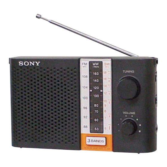
Photo : ICF-F12S
Notes on chip component replacement
•
Never reuse a disconnected chip component.
•
Notice that the minus side of a tantalum capacitor may be dam-
aged by heat.
FM/SW/MW 3 BAND RADIO
E Model
Advertisement
Table of Contents

Related Manuals for Sony ICF-F12S


Summary of Contents for Sony ICF-F12S
- Page 1 Approx. 676 g (1 lb 8 oz) incl. carrying strap and batteries Supplied accessories carrying strap (1) Design and specifications are subject to change without notice. FM/SW/MW 3 BAND RADIO Sony Corporation 9-887-911-02 2007L05-1 Audio Business Group © 2007.12 Published by Sony Techno Create Corporation...
-
Page 2: Section 1 Servicing Notes
Battery life (Approx. hours) (JEITA*) When using Note Adjust the direction of the Sony R20 (size D) antenna by holding the bottom of it. The antenna can be damaged * Measured by JEITA (Japan Electronics and when you move the antenna with Information Technology Industries Association) excessive force. -
Page 3: Section 3 Disassembly
ICF-F11S/F12S SECTION 3 DISASSEMBLY • This set can be disassembled in the order shown below. 3-1. DISASSEMBLY FLOW 3-5. GEAR (VC) AND MAIN BOARD SETTING (Page 5) 3-2. REAR CABINET BLOCK (Page 3) 3-3. MAIN BOARD, GEAR (VC) 3-4. TELESCOPIC ANTENNA (ANT1), (Page 4) BATTERY CASE LID, CABINET (REAR) (Page 4) - Page 4 ICF-F11S/F12S 3-3. MAIN BOARD, GEAR (VC) two screws MAIN board Remove a solder. gear (VC) Remove two solders. Remove a solder. 3-4. TELESCOPIC ANTENNA (ANT1), BATTERY CASE LID, CABINET (REAR) telescopic antenna (ANT1) cabinet (rear) battery case lid two bosses battery case lid cabinet (rear) cushion...
- Page 5 ICF-F11S/F12S Note: Follow the assembly procedure in the numerical order given. 3-5. GEAR (VC) AND MAIN BOARD SETTING Match two gears. Down the pointer. first concave portion Set the second concave portion of pointer to the convex part of the gear (VC). Install the gear (VC) rib of front cabinet as shown in figure.
-
Page 6: Section 4 Electrical Adjustment
ICF-F11S/F12S SECTION 4 ELECTRICAL ADJUSTMENT 0 dB=0.280 mV MW/SW IF ADJUSTMENT Adjustment for a maximum reading on level meter [MW] 455 kHz Setting: BAND switch : MW MW FREQUENCY COVERAGE ADJUSTMENT MAIN board TP (SP +) Adjustment Part Frequency Display Put the lead-wire AM RF signal antenna close to... -
Page 7: Main Board (Component Side)
ICF-F11S/F12S Adjustment Location: – MAIN BOARD (Component Side) – SW Frequency Coverage Adjustment MW/SW IF Adjustment SW Tracking Adjustment (F12S) BAND FM Tracking Adjustment CT1-3 FM Frequency Coverage Adjustment CT1-4 POWER MW Frequency Coverage Adjustment MW Tracking Adjustment CT1-2 CT1-1 –... - Page 8 ICF-F11S/F12S MEMO...
- Page 9 ICF-F11S/F12S SECTION 5 DIAGRAMS THIS NOTE IS COMMON FOR PRINTED WIRING BOARD AND SCHEMATIC DIAGRAM. 5-1. PRINTED WIRING BOARD - MAIN Board - • : Uses unleaded solder. (In addition to this, the necessary note is printed in each block.) For Printed Wiring Boards.
- Page 10 ICF-F11S/F12S 5-2. SCHEMATIC DIAGRAM - MAIN Board - • See page 9 for IC Block Diagram. TUNING S1-2 FERRITE-ROD MW OSC 220p ANTENNA CT1-1 S1-3 CT1-3 100p CT1-2 S1-4 S1-5 FM RF CV1-3 (F11S) 12μH (F11S) (F12S) SW OSC CV1-1 CV1-2 *C18 (F12S)
-
Page 11: Section 6 Exploded View
ICF-F11S/F12S SECTION 6 EXPLODED VIEW Note: • -XX and -X mean standardized parts, so • The mechanical parts with no reference • Accessories are given in the last of the they may have some difference from the number in the exploded views are not sup- electrical parts list. -
Page 12: Section 7 Electrical Parts List
ICF-F11S/F12S SECTION 7 MAIN ELECTRICAL PARTS LIST Note: • Due to standardization, replacements in • COILS When indicating parts by reference num- the parts list may be different from the uH: μH ber, please include the board name. parts specifi ed in the diagrams or the com- •... - Page 13 ICF-F11S/F12S MAIN Ref. No. Part No. Description Remark Ref. No. Part No. Description Remark 1-414-142-11 INDUCTOR 1-410-510-11 INDUCTOR 12uH (F11S) 1-412-979-21 INDUCTOR < TRANSISTOR > 8-729-620-13 TRANSISTOR 2SC4154TP-1EF < RESISTOR > 1-216-829-11 METAL CHIP 4.7K 1/10W 1-216-825-11 METAL CHIP 2.2K 1/10W 1-216-813-11 METAL CHIP...
- Page 14 ICF-F11S/F12S MEMO...
- Page 15 ICF-F11S/F12S ICF-F11S/F12S 2. DIAGRAMS THIS NOTE IS COMMON FOR PRINTED WIRING BOARD AND SCHEMATIC DIAGRAM. (In addition to this, the necessary note is printed in each block.) For Printed Wiring Boards. For Schematic Diagrams. E Model Note: Note: • X : Parts extracted from the component side. •...
- Page 16 ICF-F11S/F12S 2-1. SCHEMATIC DIAGRAM - MAIN Board - TUNING S1-2 FERRITE-ROD MW OSC 220p ANTENNA CT1-1 S1-3 CT1-3 100p CT1-2 S1-4 S1-5 FM RF CV1-3 (F11S) 12μH (F11S) (F12S) SW OSC CV1-1 CV1-2 *C18 (F12S) CV1-4 CT1-4 (F11S) 470p (F12S) (F12S) (F11S) BAND...
-
Page 17: Printed Wiring Board - Main Board
ICF-F11S/F12S 2-2. PRINTED WIRING BOARD - MAIN Board - • : Uses unleaded solder. MAIN BOARD MW FERRITE-ROD ANTENNA POWER FM OSC CT1-1 TUNING CV1-4 CV1-1 CT1-4 BAND CT1-3 MW OSC CV1-3 CV1-2 (F11S) (F12S) CT1-2 NATURAL FM RF (F12S) SW OSC L8 (F11S) BPF1... - Page 18 ICF-F11S/F12S MAIN 3. ELECTRICAL PARTS LIST Note: • Due to standardization, replacements in • COILS When indicating parts by reference num- the parts list may be different from the uH: μH ber, please include the board name. parts specifi ed in the diagrams or the com- •...
- Page 19 ICF-F11S/F12S MAIN Ref. No. Part No. Description Remark Ref. No. Part No. Description Remark 1-414-142-11 INDUCTOR 1-410-510-11 INDUCTOR 12uH (F11S) 1-412-979-21 INDUCTOR < TRANSISTOR > 8-729-620-13 TRANSISTOR 2SC4154TP-1EF < RESISTOR > 1-216-829-11 METAL CHIP 4.7K 1/10W 1-216-825-11 METAL CHIP 2.2K 1/10W 1-216-813-11 METAL CHIP...
-
Page 20: Revision History
ICF-F11S/F12S REVISION HISTORY Checking the version allows you to jump to the revised page. Also, clicking the version at the top of the revised page allows you to jump to the next revised page. Ver. Date Description of Revision 2007.11 2007.12 Change of MAIN board (Suffi...
Need help?
Do you have a question about the ICF-F12S and is the answer not in the manual?
Questions and answers